A metal/oxide/high-κ dielectric/oxide/silicon (MOHOS) planar charge trapping memory capacitor includingSiO2 as tunnel oxide, Al–HfO2 as charge trapping layer, SiO2 as blocking oxide and TaN metal gate was fabri-cated and characterized as test vehicle in the view of integration into 3D cells. The thin charge trapping layerand blocking oxide were grown by atomic layer deposition, the technique of choice for the implementation ofthese stacks into 3D structures. The oxide stack shows a good thermal stability for annealing temperature of900 °C in N2, as required for standard complementary metal–oxide–semiconductor processes. MOHOS capac-itors can be efficiently programmed and erased under the applied voltages of ±20 V to ±12 V. When com-pared to a benchmark structure including thin Si3N4 as charge trapping layer, the MOHOS cell showscomparable program characteristics, with the further advantage of the equivalent oxide thickness scalabilitydue to the high dielectric constant (κ) value of 32, and an excellent retention even for strong testingconditions. Our results proved that high-κ based oxide structures grown by atomic layer deposition can beof interest for the integration into three dimensionally stacked charge trapping devices.
Three dimensionally stacked charge trapping memory devices arenowadays considered the most viable solution in order to extend theFlash NAND technology scalability beyond 16 nm node [1]. Indeed,employing 3D architectures, such as Bit Cost Scalable (BiCS) [2] orterabit cell array transistor [3], which are based on Si/SiO2/Si3N4/SiO2/Si (SONOS) structures, it is possible to improve the device performance,due to the geometrical effect, by breaking the erase/retention trade offwith respect to the SONOS planar structures. Further, 3D architecturesallow increasing the bit density while considerably reducing bit costin NAND Flash memories.
Considering for instance the BiCS structure [2], the curvature of acylindrical SONOS cell has the effect of increasing the electric fielddrop across the SiO2 tunnel oxide while decreasing the electric fieldacross the SiO2 blocking oxide during both program and erase opera-tions. In this way, the performance of the device is improved, andthere is no need to introduce a high dielectric constant (high-κ) ma-terial as blocking oxide, as required in planar geometry (e.g. TANOScell [1,4,5]). Besides, a good retention of the 3D SONOS cell is ensuredby the high barrier heights for trapped electrons provided by the SiO2
tunnel and blocking oxides.
t (G. Congedo),
rights reserved.
A critical aspect concerns the thickness of each layer composingthe ONO stack, which must be thin enough to fit into narrow cylinderholes, with a good conformality. Further, better performing materialscould be introduced instead of Si3N4 as charge trapping layer in orderto further improve the program/erase and retention behavior of thedevice and to decrease the total equivalent oxide thickness (EOT) ofthe stack.
In this work, we propose a SONOS-like planar capacitor, includinga high-κ Al–HfO2 as charge trapping layer and SiO2 as blocking oxide(MOHOS cell), both grown by atomic layer deposition (ALD), as a testvehicle for the evaluation of the feasibility of high-κ based stacks forfuture integration into 3D Flash memories. ALD was chosen becauseit ensures the thin film uniformity and conformality on the cylinderholes required in 3D SONOS cells. Al–HfO2 was selected as thecharge trapping layer because of its high κ value due to the Al incor-poration into HfO2 during ALD process, as found in our case (κ valueof 32) and in other studies reported in the literature [6]. Indeed, acharge trapping layer with κ value as high as possible allows maximiz-ing the electric field drop through the tunnel oxide during program/erase [7–9]. Even if poly-Si is used as gate electrode of 3D cells, wechose for our test vehicle a high work function metal gate such as TaN(work function of 5.3 eV [10]) in order to minimize the electron injec-tion from the gate towards the charge trapping layer during eraseoperation.
By means of chemical and structural analyses we checked the Alcontent, and the thermal stability of the oxide stacks before and
10 G. Congedo et al. / Thin Solid Films 533 (2013) 9–14
after rapid thermal annealing (RTA) at 900 °C, as well as the temper-ature dependence of the high-κ oxide crystallographic structure.MOHOS capacitors were electrically characterized by means ofprogram/erase and retention measurements, and a benchmarkingwith a reference sample including Si3N4 as charge trapping layer(MONOS), fabricated under similar condition, was also provided.
2. Experimental details
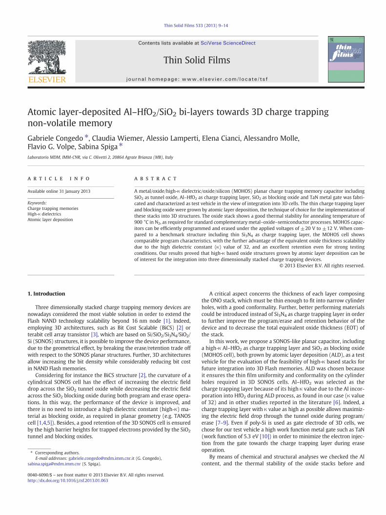
Fig. 1(a) and (b) show the sketch of MOHOS and MONOS capaci-tors analyzed in this work. For both the analyzed stacks, the startingsubstrate was a 4.5 nm thick thermal SiO2, used as tunnel oxide, ontop of Si (100). Then, for MOHOS stacks, 8.5 nm thick Al–HfO2 chargetrapping layer and 8.0 nm thick SiO2 blocking oxide were grown byALD at 300 °C in a Savannah 200 reactor (Cambridge Nanotech Inc.).MeCp2HfMe(OMe)Hf, Al(CH3)3 and O3 were used as Hf, Al and oxy-gen precursors, respectively, and the Al:Hf ratio during each ALDsupercycle was set to 1:20. SiO2 blocking oxide was deposited usingH2Si[N(C2H5)2]2 and O3 as Si and oxygen sources, respectively, with-out breaking the vacuum into the deposition chamber. After deposi-tion the stacks were subjected to RTA at 900 °C for 60 s in N2
ambient. The capacitor fabrication was completed by UV lithography,15 nm TaN/30 nm W sputtering deposition and a lift-off process. Ca-pacitors (with gate areas of 8×10⁻⁴ cm2) were then subjected to aRTA at 900 °C in N2 and a forming gas (Ar+4% H2) annealing at400 °C for 15 min. MONOS reference sample including 6.0 nm thickSi3N4 made by low-pressure chemical vapor deposition and 8.0 nmthick SiO2 made by ALD was then fabricated, and exposed to thesame thermal treatments as in the case of MOHOS.
The film composition was analyzed by X-ray photoelectron spec-troscopy (XPS), while the structural properties of the as-depositedand annealed oxide stacks were studied by means of grazing inci-dence X-ray diffraction (GIXRD) and X-ray reflectivity (XRR), beforemetallization. XPS was generated by a standard Mg Kα (1253.6 eV)source with a take-off-angle (TOA) of 70°. Sufficiently thick films(8.5 nm) were used to avoid interface effects. Photoelectrons wererecorded in an Omicron EA 125 HR analyzer (endowed with anangle acceptance of 68° in the high-resolution mode) using a pass en-ergy of 20 eV, an energy step size of 0.05 eV, and a dwell time of 0.5 sduring acquisition of single XPS lines. GIXRD and XRR analyses wereperformed in an upgraded XRD-3000 diffractometer (Italstructures),in the same configuration as in Ref. [11]. Data fitting was performedusing MAUD program [12]. Chemical properties of the oxide stacksand in particular the thermal stability of the different layers uponRTA were further addressed by time of flight-secondary ion massspectrometry (ToF-SIMS) depth profiles. ToF-SIMS measurements
Fig. 1. Sketch of the (a) MOHOS and (b) MONOS capacitors analyzed in this paper. Thethickness indicated in the figure is that of the annealed stacks (see also Table 1).
were performed on as-deposited and annealed stacks in a ION-TOFIV instrument (Ion ToF GmbH) using Cs+ sputtering ions with energyE=0.5 keV and Ga+ analyzing ions at energy E=25 keV, operatingin interlaced mode. Secondary ions were collected in negative polar-ity, and the intensity was normalized to 30Si signal in the bulk Sisubstrate.
Capacitance–voltage (C–V) measurements were acquired at dif-ferent frequencies (1 kHz–1 MHz) on MOHOS and MONOS capacitorsin a dark probe station. The EOT of the stacks was extracted by simu-lating the C–V curves at 100 kHz using the MISFIT software, whichtakes into account quantum-mechanical corrections [13]. Programand erase measurements were acquired on capacitors by monitoringthe flat band voltage shift (ΔVFB) of the C–V curves after applyingpositive (for program) or negative (for erase) voltage pulses to thegate electrodes in a pulse time range of 1 μs to 100 ms. Retentionmeasurements at room temperature and 150 °C were acquired bymonitoring the ΔVFB of the C–V curves of the capacitors after pro-gramming the cells to a given program ΔVFB level. The instrumentsemployed for electrical analysis were a HP4284A LCR meter, anAgilent 8110A pulse/pattern generator and an Agilent B1500 semi-conductor analyzer.
3. Results and discussion
3.1. Film composition and structural properties
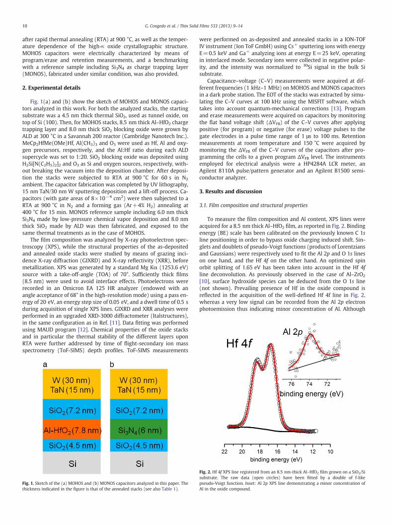
To measure the film composition and Al content, XPS lines wereacquired for a 8.5 nm thick Al–HfO2 film, as reported in Fig. 2. Bindingenergy (BE) scale has been calibrated on the previously known C 1sline positioning in order to bypass oxide charging induced shift. Sin-glets and doublets of pseudo-Voigt functions (products of Lorentziansand Gaussians) were respectively used to fit the Al 2p and O 1s lineson one hand, and the Hf 4f on the other hand. An optimized spinorbit splitting of 1.65 eV has been taken into account in the Hf 4fline deconvolution. As previously observed in the case of Al–ZrO2
[10], surface hydroxide species can be deduced from the O 1s line(not shown). Prevailing presence of Hf in the oxide compound isreflected in the acquisition of the well-defined Hf 4f line in Fig. 2,whereas a very low signal can be recorded from the Al 2p electronphotoemission thus indicating minor concentration of Al. Although
Fig. 2. Hf 4f XPS line registered from an 8.5 nm-thick Al–HfO2 film grown on a SiO2/Sisubstrate. The raw data (open circles) have been fitted by a double of f-likepseudo-Voigt function. Inset: Al 2p XPS line demonstrating a minor concentration ofAl in the oxide compound.
Table 1Thickness, electron density and surface roughness of the deposited layers before andafter annealing. The error on thickness and roughness is ±0.1 nm, the error on elec-tron density is ±0.05 e−/Å3.
11G. Congedo et al. / Thin Solid Films 533 (2013) 9–14
the Al 2p line signal is quite at the edge of the XPS sensitivity, theatomic composition of the oxide can be estimated from the proposedfit to the Hf 4f, Al 2p, and O 1s XPS lines upon normalizing on the rel-evant atomic sensitivity factors [14]. The so-deduced concentration ofAl in the oxide results in between 4.5% (if the hydroxide contributionis neglected) to 4.9% (if the hydroxide contribution is taken intoaccount).
XRR data and simulation of the as-deposited and annealed stacksincluding Al–HfO2 are shown in Fig. 3. Table 1 provides the thickness,electron density and surface roughness of the as-deposited layers,extracted from XRR data fitting. The analysis was performed on thesame piece before and after annealing. A thickness reduction of 10%and 8% for SiO2 and Al–HfO2, respectively is measured after RTA.The electron density of the SiO2 layer is compatible with the one ofa densified SiO2 and does not vary with annealing. The electrondensity of the Al–HfO2 layer increases after RTA.
GIXRD pattern acquired on SiO2/Al–HfO2/SiO2/Si stacks after RTAat 900 °C in N2 is shown in Fig. 4. The as-deposited Al–HfO2 film isamorphous, whereas after RTA it becomes crystallized. The diffractedpeaks might correspond to both the cubic and tetragonal polymorphsof HfO2. No diffraction peak related to the monoclinic phase of HfO2
was detected. The experimental data were simulated by Rietveldrefinement starting from the cubic fluorite structure of HfO2. Asshown in Fig. 4, the position of the diffracted maxima is differentfrom the one reported for the powder spectrum and corresponds toa lower lattice parameter. The lattice parameter value extractedfrom the Rietveld refinement when considering the cubic structureis a=4.99 Å. Differently, in the case of pure HfO2, grown with thesame ALD recipe used in this work but without Al doping, GIXRDmeasurements revealed the presence of the monoclinic phase ofHfO2 both in as-deposited and annealed at 900 °C in N2 films[15,16]. Therefore, our results confirm the role of Al doping in stabiliz-ing the cubic and/or tetragonal polymorphs.
Fig. 5 shows ToF-SIMS depth profiles acquired on the oxide stacksincluding either Al–HfO2 (Fig. 5(a)) or Si3N4 (Fig. 5(b)) as chargetrapping layer, evidencing the thermal stability of both stacks uponRTA treatment. Indeed, in both cases, the different layers composingeach stack are well identified by the respective negative ions, withsharp interfaces. In particular, when considering the intensity of 30Siacross Al–HfO2/SiO2 (bottom) interface in Fig. 4(a) the intensity ofthe as-deposited and annealed samples well overlaps, indicatingthat Al–HfO2/SiO2 interface is preserved upon annealing at 900 °C. Itshould be mentioned that the seeming Al tail extending into bottomSiO2 is the result of the knock-on sputtering effect during the profilinganalysis [17]; from its linear decay (in logscale) down to backgroundintensity, no evidence of Al diffusion in bottom SiO2 is detected.
Fig. 3. XRR data (dots) and simulation (lines) of as deposited (lower curves) andannealed (upper curves) Si/SiO2/Al–HfO2/SiO2 stacks.
Furthermore, SiO2/Al–HfO2 (top) interface is marginally affected byRTA at 900 °C, as indicated by the Al and HfO ion intensity. It is alsorelevant to note that after annealing no Si diffusion in the Al–HfO2
layer, nor Al or Hf diffusion in top or bottom SiO2 layers is evidenced,thus indicating that the integration of Al–HfO2 is compatible with astandard CMOS process employed for the fabrication of 3D-stackedFlash memories. Further, Al and HfO ion intensity is almost flat inAl–HfO2, which excludes the partial segregation of Al in HfO2 and in-dicates that Al doping is uniformly distributed through the entirelayer thickness. When considering ToF-SIMS depth profiles of refer-ence sample in Fig. 5(b) the thermal stability at 900 °C is clear, as pro-files of 30Si and SiN ions of the as-deposited and annealed samples arewell overlapped from the sample surface down to Si substrate, and inparticular along the interfaces, where no traces of interdiffusion arevisible.
3.2. Electrical characterization
In order to extract the dielectric constant value of the crystallizedAl–HfO2 films, layers with different thickness were grown on the4.5 nm SiO2/Si substrate and annealed at 900 °C. From the slope ofstack EOT versus Al–HfO2 physical thickness (Fig. 6), the extracted κvalue is 32±1 while the intercept with the y-axis gives the expectedEOT value of the bottom SiO2. The measured κ value corroborateswith the structural properties, since the cubic and tetragonal phasesare associated with HfO2 high-κ values [18]. It is worth noticing thatthe measured κ value is significantly higher than the one measuredfor the binary HfO2 compound (κ~16) in the monoclinic phase[15,16]. The measured value is also comparable to the one measuredfor cubic-Er-HfO2 [19], but higher than κ=27, as measured forAl–ZrO2 (with 9.7% Al). The high κ value measured for Al–HfO2 in thiswork is therefore the result of the stabilization of the cubic phase aswell as the Al low doping concentration (b5%). It is worth noticing
Fig. 4. GIXRD pattern acquired on Si/SiO2/Al–HfO2/SiO2 stack after RTA at 900 °C in N2.
Fig. 5. ToF-SIMS depth profiles acquired on as-deposited and annealed (a) SiO2/Al–HfO2/SiO2/Si and (b) SiO2/Si3N4/SiO2/Si stacks.
Fig. 6. Plot of EOT vs. Al–HfO2 thickness of TaN/Al–HfO2/4.5 nm SiO2/Si capacitors in-cluding annealed Al–HfO2 films with different thickness. The κ value of Al–HfO2 isextracted from the slope of the linear fit of experimental data.
12 G. Congedo et al. / Thin Solid Films 533 (2013) 9–14
that also for the rare earth doped HfO2 system [20], the κ value has beenfound to be related to the dopant concentration, type of dopant andpost-deposition annealing temperature.
The Al–HfO2 film has been therefore integrated in the MOHOSmemory cell as charge trapping layer, and compared to the MONOS
Fig. 7. (a) C–V characteristics acquired at 1 MHz of the MOHOS (continuous line) andMONOgate voltage pulses on the MOHOS and MONOS stacks.
reference sample integrating the more standard and widely studiedSi3N4 charge trapping layer. The C–V characteristics acquired at1 MHz on MOHOS and MONOS cells (Fig. 1) in the fresh state areshown in Fig. 7(a). C–V curves do not show any frequency dispersionin the accumulation region and negligible hysteresis (not shown).
The EOT values extracted from the simulation of the C–V curvesusing MISFIT are 12.6 nm and 15.3 nm for MOHOS and MONOS stacks,respectively. These values are well consistent with the expected onesconsidering the κ values of the various layers (κ value of 6–7 and 32for Si3N4 and Al–HfO2, respectively), and therefore our results demon-strate that using a material with κ value higher than Si3N4 allows agreat reduction of the total EOT of the stack for similar thicknesses ofthe charge trapping layer, this result being encouraging for extendingthe scalability of charge trapping memories towards ultra-scaled tech-nology nodes [1].
Fig. 7(b) shows program transients, acquired at different gate volt-age pulses, on the MOHOS and MONOS stacks annealed at 900 °C inN2. The devices can be efficiently programmed under typical operat-ing conditions, i.e. applied voltages in the +20 V to +12 V rangefor pulse times of 1 μs–100 ms, and large VFB shifts are achievedwhen applying high voltage pulses. When comparing program tran-sients of the MOHOS and MONOS stacks, it is demonstrated that forhigh program voltages (20 V) the MOHOS stack has a better programspeed than the benchmark sample including Si3N4 charge trappinglayer. This could be related to the effect of the high κ value of Al–HfO2
(more than five times higher than Si3N4), which allows, in theMOHOS device, a higher electric field drop through the SiO2 tunneloxide under Fowler–Nordheim tunneling conditions with respect tothe MONOS reference sample for the same applied voltage. For exam-ple, in the case of the transients acquired at 20 V shown in Fig. 7(b)the electric field drop on the SiO2 tunnel oxide is 15.5 MV/cm and13.4 MV/cm for MOHOS and MONOS stacks, respectively. As alsoshown in same Fig. 7(b), at 18 V the transients of the two stacks arerather comparable, whereas at lower applied gate pulses (16 V andbelow) the ΔVFB levels of the MOHOS stack for pulse times higherthan 100 μs are slightly lower than the MONOS reference. This couldbe due to a slightly lower program efficiency (considered as the ratiobetween the trapped charge and the total injected charge in the stack)of the MOHOS stack than the MONOS one. However, this does not sig-nificantly compromise the program performance of theMOHOS device,since for typical pulse times at which a NAND Flash memory operates(i.e. 100 μs and below) the program ΔVFB levels of the two devices arenearly the same.
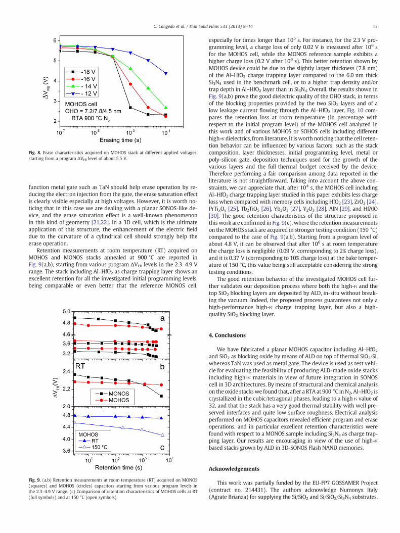
Erase characteristics of MOHOS device are shown in Fig. 8. Startingfrom a program ΔVFB level of ~5.5 V, it is shown that under the neg-ative applied voltages of −18 V to −12 V the cell can be erased;moreover, for applied voltage of −20 V, a steep ΔVFB is observedfor a pulse time of 1 ms. Even though the presence of a high work
S (dashed line) capacitors in the fresh state. (b) Program transients acquired at different
Fig. 8. Erase characteristics acquired on MOHOS stack at different applied voltages,starting from a program ΔVFB level of about 5.5 V.
13G. Congedo et al. / Thin Solid Films 533 (2013) 9–14
function metal gate such as TaN should help erase operation by re-ducing the electron injection from the gate, the erase saturation effectis clearly visible especially at high voltages. However, it is worth no-ticing that in this case we are dealing with a planar SONOS-like de-vice, and the erase saturation effect is a well-known phenomenonin this kind of geometry [21,22]. In a 3D cell, which is the ultimateapplication of this structure, the enhancement of the electric fielddue to the curvature of a cylindrical cell should strongly help theerase operation.
Retention measurements at room temperature (RT) acquired onMOHOS and MONOS stacks annealed at 900 °C are reported inFig. 9(a,b), starting from various program ΔVFB levels in the 2.3–4.9 Vrange. The stack including Al–HfO2 as charge trapping layer shows anexcellent retention for all the investigated initial programming levels,being comparable or even better that the reference MONOS cell,
Fig. 9. (a,b) Retention measurements at room temperature (RT) acquired on MONOS(squares) and MOHOS (circles) capacitors starting from various program levels inthe 2.3–4.9 V range. (c) Comparison of retention characteristics of MOHOS cells at RT(full symbols) and at 150 °C (open symbols).
especially for times longer than 105 s. For instance, for the 2.3 V pro-gramming level, a charge loss of only 0.02 V is measured after 106 sfor the MOHOS cell, while the MONOS reference sample exhibits ahigher charge loss (0.2 V after 106 s). This better retention shown byMOHOS device could be due to the slightly larger thickness (7.8 nm)of the Al–HfO2 charge trapping layer compared to the 6.0 nm thickSi3N4 used in the benchmark cell, or to a higher trap density and/ortrap depth in Al–HfO2 layer than in Si3N4. Overall, the results shown inFig. 9(a,b) prove the good dielectric quality of the OHO stack, in termsof the blocking properties provided by the two SiO2 layers and of alow leakage current flowing through the Al–HfO2 layer. Fig. 10 com-pares the retention loss at room temperature (in percentage withrespect to the initial program level) of the MOHOS cell analyzed inthis work and of various MOHOS or SOHOS cells including differenthigh-κ dielectrics, from literature. It isworth noticing that the cell reten-tion behavior can be influenced by various factors, such as the stackcomposition, layer thicknesses, initial programming level, metal orpoly-silicon gate, deposition techniques used for the growth of thevarious layers and the full-thermal budget received by the device.Therefore performing a fair comparison among data reported in theliterature is not straightforward. Taking into account the above con-straints, we can appreciate that, after 104 s, the MOHOS cell includingAl–HfO2 charge trapping layer studied in this paper exhibits less chargeloss when compared with memory cells including HfO2 [23], ZrO2 [24],PrTixOy [25], Tb2TiO5 [26], Yb2O3 [27], Y2O3 [28], AlN [29], and HfAlO[30]. The good retention characteristics of the structure proposed inthiswork are confirmed in Fig. 9(c), where the retentionmeasurementson theMOHOS stack are acquired in stronger testing condition (150 °C)compared to the case of Fig. 9(a,b). Starting from a program level ofabout 4.8 V, it can be observed that after 106 s at room temperaturethe charge loss is negligible (0.09 V, corresponding to 2% charge loss),and it is 0.37 V (corresponding to 10% charge loss) at the bake temper-ature of 150 °C, this value being still acceptable considering the strongtesting conditions.
The good retention behavior of the investigated MOHOS cell fur-ther validates our deposition process where both the high-κ and thetop SiO2 blocking layers are deposited by ALD, in-situ without break-ing the vacuum. Indeed, the proposed process guarantees not only ahigh-performance high-κ charge trapping layer, but also a high-quality SiO2 blocking layer.
4. Conclusions
We have fabricated a planar MOHOS capacitor including Al–HfO2
and SiO2 as blocking oxide by means of ALD on top of thermal SiO2/Si,whereas TaN was used as metal gate. The device is used as test vehi-cle for evaluating the feasibility of producing ALD-made oxide stacksincluding high-κ materials in view of future integration in SONOScell in 3D architectures. By means of structural and chemical analysison the oxide stackswe found that, after a RTA at 900 °C in N2, Al–HfO2 iscrystallized in the cubic/tetragonal phases, leading to a high κ value of32, and that the stack has a very good thermal stability with well pre-served interfaces and quite low surface roughness. Electrical analysisperformed on MOHOS capacitors revealed efficient program and eraseoperations, and in particular excellent retention characteristics werefound with respect to a MONOS sample including Si3N4 as charge trap-ping layer. Our results are encouraging in view of the use of high-κbased stacks grown by ALD in 3D-SONOS Flash NAND memories.
Acknowledgements
This work was partially funded by the EU-FP7 GOSSAMER Project(contract no. 214431). The authors acknowledge Numonyx Italy(Agrate Brianza) for supplying the Si/SiO2 and Si/SiO2/Si3N4 substrates.
Fig. 10. Comparison among the charge loss (in percentage) at room temperature after 104 s for different MONOS/SONOS-like devices including different high-κ dielectrics as chargetrapping layer. For each reference the layer thickness (nm), gate material and initial programming levels are indicated in the following format: tunnel oxide/charge-trap/blockingoxide/gate [initial ΔVFB, this parameter is reported only when available].
14 G. Congedo et al. / Thin Solid Films 533 (2013) 9–14
References
[1] The International Technology Roadmap for Semiconductors 2011 Edition, http://www.itrs.net.
[2] H. Aochi, Very Large Scale Integration Technology Symposium Proceedings, 2007,p. 1.
[3] J. Jang, H.-S. Kim, W. Cho, H. Cho, J. Kim, S.I. Shim, Y. Jang, J.-H. Jeong, B.-K. Son,D.W. Kim, K. Kim, J.-J. Shim, J.S. Lim, K.-H. Kim, S.Y. Yi, J.-Y. Lim, D. Chung, H.-C.Moon, S. Hwang, J.-W. Lee, Y.-H. Son, U.-I. Chung, W.-S. Lee, Very Large ScaleIntegration Technology Symposium Proceedings, 2009, p. 192.
[4] C.H. Lee, K.I. Choi, M.K. Cho, Y.H. Song, K.C. Park, K. Kim, International ElectronDevice Meeting Proceedings, 2003, p. 613.
[5] C.H. Lee, K.C. Park, K. Kim, Appl. Phys. Lett. 87 (2005) 073510.[6] P.K. Park, S.-W. Kang, Appl. Phys. Lett. 89 (2006) 192905.[7] G. Congedo, A. Lamperti, L. Lamagna, S. Spiga, Microelectron. Eng. 88 (2011) 1174.[8] A. Cacciato, A. Suhane, O. Richard, A. Arreghini, C. Adelmann, J. Swerts, A. Rothschild,
G. Van den bosch, L. Breuil, H. Bender, M. Jurczak, I. Debusschere, J.A. Kittl, J. VanHoudt, European Solid State Device Research Conference Proceedings, 2010,p. 436.
[10] S. Spiga, R. Rao, L. Lamagna, C. Wiemer, G. Congedo, A. Lamperti, A. Molle,M. Fanciulli, F. Palma, F. Irrera, J. Appl. Phys. 112 (2012) 014107.
[11] A. Lamperti, L. Lamagna, G. Congedo, S. Spiga, J. Electrochem. Soc. 158 (2011)G221.
[12] L. Lutterotti, S. Matthies, H.-R. Wenk, IUCr Newsletter of the CPD, 21, 1999, p. 14,(http://www.ing.unitn.it/~maud/).
[13] G. Apostolopoulos, G. Vellianitis, A. Dimoulas, J.C. Hooker, T. Conard, Appl. Phys.Lett. 84 (2004) 260.
[14] D. Brigg, M.P. Seah, 1st ed., Auger and X-ray Photoelectron Spectroscopy, PracticalSurface Analysis, vol. 1, Wiley, New York, 1990, p. 635.
[15] S. Spiga, G. Congedo, U. Russo, A. Lamperti, O. Salicio, F. Driussi, E. Vianello, Proc.European Solid State Device Research Conference Proceedings, 2010, p. 408.
[16] S. Spiga, F. Driussi, A. Lamperti, G. Congedo, O. Salicio, Appl. Phys. Express 5(2012) 021102.
[17] A. Lamperti, E. Cianci, O. Salicio, L. Lamagna, S. Spiga, M. Fanciulli, Surf. InterfaceAnal. 45 (2013) 390.
[18] X. Zhao, D. Vanderbilt, Phys. Rev. B 65 (2002) 075105.[19] C. Wiemer, L. Lamagna, S. Baldovino, M. Perego, S. Schamm-Chardon, P.E. Coulon,
O. Salicio, G. Congedo, S. Spiga, M. Fanciulli, Appl. Phys. Lett. 96 (2010) 182901.[20] S. Govindarajan, T.S. Böscke, P. Sivasubramani, P.D. Kirsch, B.H. Lee, H.-H. Tseng, R.
Jammy, U. Schröder, S. Ramanathan, B.E. Gnade, Appl. Phys. Lett. 91 (2007)062906.
[21] L. Breuil, G. Van den bosch, A. Cacciato, L. Date, G.S. Kar, B. Tang, A. Arreghini,I. Debusschere, J. Van Houdt, Microelectron. Eng. 88 (2011) 1164.
[22] S. Jeon, J.H. Han, J. Lee, S. Choi, H. Hwang, C. Kim, IEEE Electron Device Lett. 27(2006) 486.