This article appeared in a journal published by Elsevier. The attached copy is furnished to the author for internal non-commercial research and education use, including for instruction at the authors institution and sharing with colleagues. Other uses, including reproduction and distribution, or selling or licensing copies, or posting to personal, institutional or third party websites are prohibited. In most cases authors are permitted to post their version of the article (e.g. in Word or Tex form) to their personal website or institutional repository. Authors requiring further information regarding Elsevier’s archiving and manuscript policies are encouraged to visit: http://www.elsevier.com/copyright
Transcript
This article appeared in a journal published by Elsevier. The attachedcopy is furnished to the author for internal non-commercial researchand education use, including for instruction at the authors institution
and sharing with colleagues.
Other uses, including reproduction and distribution, or selling orlicensing copies, or posting to personal, institutional or third party
websites are prohibited.
In most cases authors are permitted to post their version of thearticle (e.g. in Word or Tex form) to their personal website orinstitutional repository. Authors requiring further information
regarding Elsevier’s archiving and manuscript policies areencouraged to visit:
Contents lists available at SciVerse ScienceDirect
Sensors and Actuators A: Physical
j ourna l h o me pa ge: www.elsev ier .com/ locate /sna
Enhancing displacement of lead–zirconate–titanate (PZT) thin-film membranemicroactuators via a dual electrode design
Chuan Luoa, G.Z. Caob, I.Y. Shena,∗
a Department of Mechanical Engineering, University of Washington, Seattle, WA 98195-2600, USAb Department of Material Science & Engineering, University of Washington, Seattle, WA 98195-2120, USA
a r t i c l e i n f o
Article history:Received 25 May 2011Received in revised form 11 October 2011Accepted 21 October 2011Available online 25 October 2011
Keywords:PZT thin filmsMicro-actuatorsDual electrodesFinite element analyses
a b s t r a c t
A common design of piezoelectric microactuators adopts a membrane structure that consists of a base sil-icon diaphragm, a layer of bottom electrode, a layer of piezoelectric thin film, and a layer of top electrode.In particular, the piezoelectric thin film is often made of lead–zirconate–titanate (PZT) for its high piezo-electric constants. When driven electrically, the PZT thin film extends or contracts flexing the membraneand generating an out-of-plane displacement. Many manufacturing defects, however, could significantlyreduce the designed actuator displacement. Examples include residual stresses, warping, non-uniformetching of the silicon diaphragm, and misalignment between the top electrode and the silicon diaphragm.The purpose of this paper is to develop a dual top-electrode design to enhance the actuator displacement.In this design, the top electrode consists of two disconnected (thus independent) electrode areas, whilea continuous bottom electrode serves as the ground. The two top electrodes are located in two regionswith opposite curvature when the diaphragm deflects. When the two top electrodes are driven in anout-of-phase manner, the actuator displacement is enhanced. Finite element analyses and experimen-tal measurements both confirm the feasibility of this design. When manufacturing defects are present,experimental results indicate that the actuator displacement can be optimized by adjusting the phasedifference between the dual top electrodes.
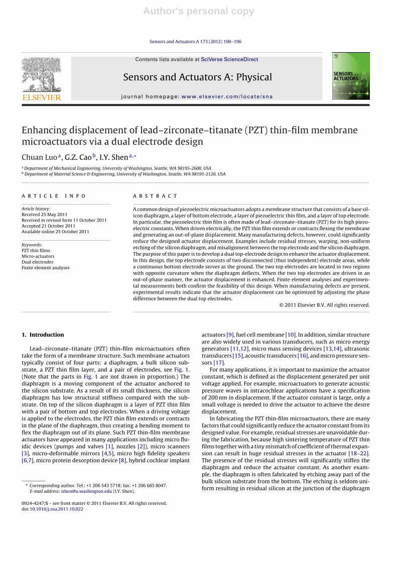
Lead–zirconate–titanate (PZT) thin-film microactuators oftentake the form of a membrane structure. Such membrane actuatorstypically consist of four parts: a diaphragm, a bulk silicon sub-strate, a PZT thin film layer, and a pair of electrodes, see Fig. 1.(Note that the parts in Fig. 1 are not drawn in proportion.) Thediaphragm is a moving component of the actuator anchored tothe silicon substrate. As a result of its small thickness, the silicondiaphragm has low structural stiffness compared with the sub-strate. On top of the silicon diaphragm is a layer of PZT thin filmwith a pair of bottom and top electrodes. When a driving voltageis applied to the electrodes, the PZT thin film extends or contractsin the plane of the diaphragm, thus creating a bending moment toflex the diaphragm out of its plane. Such PZT thin-film membraneactuators have appeared in many applications including micro flu-idic devices (pumps and valves [1], nozzles [2]), micro scanners[3], micro-deformable mirrors [4,5], micro high fidelity speakers[6,7], micro protein desorption device [8], hybrid cochlear implant
actuators [9], fuel cell membrane [10]. In addition, similar structureare also widely used in various transducers, such as micro energygenerators [11,12], micro mass sensing devices [13,14], ultrasonictransducers [15], acoustic transducers [16], and micro pressure sen-sors [17].
For many applications, it is important to maximize the actuatorconstant, which is defined as the displacement generated per unitvoltage applied. For example, microactuators to generate acousticpressure waves in intracochlear applications have a specificationof 200 nm in displacement. If the actuator constant is large, only asmall voltage is needed to drive the actuator to achieve the desiredisplacement.
In fabricating the PZT thin-film microactuators, there are manyfactors that could significantly reduce the actuator constant from itsdesigned value. For example, residual stresses are unavoidable dur-ing the fabrication, because high sintering temperature of PZT thinfilms together with a tiny mismatch of coefficient of thermal expan-sion can result in huge residual stresses in the actuator [18–22].The presence of the residual stresses will significantly stiffen thediaphragm and reduce the actuator constant. As another exam-ple, the diaphragm is often fabricated by etching away part of thebulk silicon substrate from the bottom. The etching is seldom uni-form resulting in residual silicon at the junction of the diaphragm
C. Luo et al. / Sensors and Actuators A 173 (2012) 190– 196 191
Fig. 1. Schematic drawing of PZT thin-film membrane actuator (not to scale).
and the silicon substrate [18]. The residual silicon increases thediaphragm thickness and stiffens the actuator thus reducing theactuator constant.
To increase the actuator constant, the current practice is to opti-mize relative size of the top electrode to the residual silicon [18].Both simulation and experimental results indicate that the actuatorconstant reaches its maximum when the size of the top electrode isroughly 60% of the size of the residual silicon. This design, however,has several drawbacks. First, this design has only one top electrodespanning partially over the diaphragm structure. Therefore, the realestate of the actuator is not fully utilized to increase the actuatorconstant. Second, the top electrode is optimized with respect to theresidual silicon, which may vary from batch to batch depending onfabrication conditions. Therefore, the design is somewhat “passive”and lacks flexibility in adapting to various fabrication conditions.
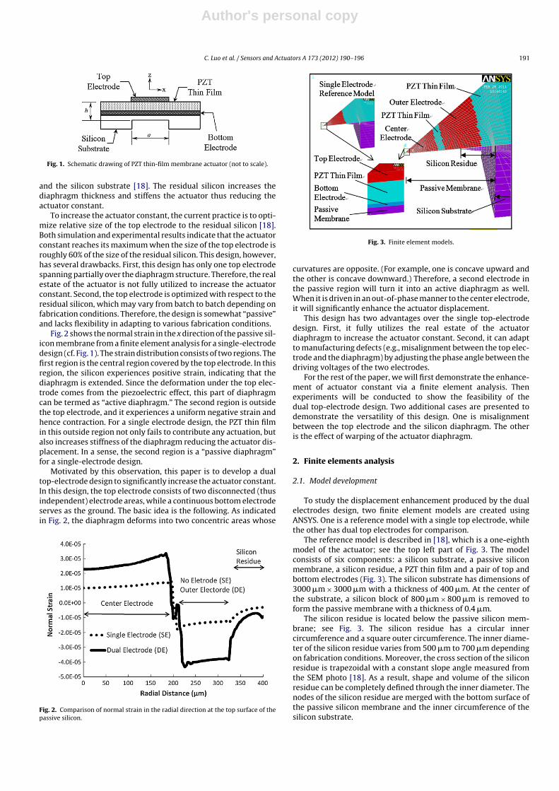
Fig. 2 shows the normal strain in the x direction of the passive sil-icon membrane from a finite element analysis for a single-electrodedesign (cf. Fig. 1). The strain distribution consists of two regions. Thefirst region is the central region covered by the top electrode. In thisregion, the silicon experiences positive strain, indicating that thediaphragm is extended. Since the deformation under the top elec-trode comes from the piezoelectric effect, this part of diaphragmcan be termed as “active diaphragm.” The second region is outsidethe top electrode, and it experiences a uniform negative strain andhence contraction. For a single electrode design, the PZT thin filmin this outside region not only fails to contribute any actuation, butalso increases stiffness of the diaphragm reducing the actuator dis-placement. In a sense, the second region is a “passive diaphragm”for a single-electrode design.
Motivated by this observation, this paper is to develop a dualtop-electrode design to significantly increase the actuator constant.In this design, the top electrode consists of two disconnected (thusindependent) electrode areas, while a continuous bottom electrodeserves as the ground. The basic idea is the following. As indicatedin Fig. 2, the diaphragm deforms into two concentric areas whose
Fig. 2. Comparison of normal strain in the radial direction at the top surface of thepassive silicon.
Fig. 3. Finite element models.
curvatures are opposite. (For example, one is concave upward andthe other is concave downward.) Therefore, a second electrode inthe passive region will turn it into an active diaphragm as well.When it is driven in an out-of-phase manner to the center electrode,it will significantly enhance the actuator displacement.
This design has two advantages over the single top-electrodedesign. First, it fully utilizes the real estate of the actuatordiaphragm to increase the actuator constant. Second, it can adaptto manufacturing defects (e.g., misalignment between the top elec-trode and the diaphragm) by adjusting the phase angle between thedriving voltages of the two electrodes.
For the rest of the paper, we will first demonstrate the enhance-ment of actuator constant via a finite element analysis. Thenexperiments will be conducted to show the feasibility of thedual top-electrode design. Two additional cases are presented todemonstrate the versatility of this design. One is misalignmentbetween the top electrode and the silicon diaphragm. The otheris the effect of warping of the actuator diaphragm.
2. Finite elements analysis
2.1. Model development
To study the displacement enhancement produced by the dualelectrodes design, two finite element models are created usingANSYS. One is a reference model with a single top electrode, whilethe other has dual top electrodes for comparison.
The reference model is described in [18], which is a one-eighthmodel of the actuator; see the top left part of Fig. 3. The modelconsists of six components: a silicon substrate, a passive siliconmembrane, a silicon residue, a PZT thin film and a pair of top andbottom electrodes (Fig. 3). The silicon substrate has dimensions of3000 �m × 3000 �m with a thickness of 400 �m. At the center ofthe substrate, a silicon block of 800 �m × 800 �m is removed toform the passive membrane with a thickness of 0.4 �m.
The silicon residue is located below the passive silicon mem-brane; see Fig. 3. The silicon residue has a circular innercircumference and a square outer circumference. The inner diame-ter of the silicon residue varies from 500 �m to 700 �m dependingon fabrication conditions. Moreover, the cross section of the siliconresidue is trapezoidal with a constant slope angle measured fromthe SEM photo [18]. As a result, shape and volume of the siliconresidue can be completely defined through the inner diameter. Thenodes of the silicon residue are merged with the bottom surface ofthe passive silicon membrane and the inner circumference of thesilicon substrate.
Author's personal copy
192 C. Luo et al. / Sensors and Actuators A 173 (2012) 190– 196
The silicon substrate, passive silicon membrane and siliconresidue are all meshed with 3D linearly elastic solid elements. Thebottom surface of the silicon substrate is subjected to geometricallyfixed boundary conditions.
On top of the passive silicon membrane there is a PZT thin filmsandwiched between a bottom electrode and a top electrode. Inaddition, the bottom surface of the bottom electrode is fixed tothe top surface of the passive membrane; see Fig. 3. The PZT thinfilm, top electrode and bottom electrode has a thickness of 1 �m,0.2 �m and 0.5 �m, respectively. The PZT thin film and the bottomelectrode span the entire top surface of the actuator, whereas thetop electrode occupies an area of 400 �m × 400 �m at the center ofthe passive membrane (on the top surface of the PZT thin film).
The PZT thin film is meshed with 3D coupled field solid ele-ments that couple electric, piezoelectric, and structural fields. Theelectrical potential of the nodes interfacing the top electrode is cou-pled together. A constant voltage is applied to serve as an electricalboundary condition. An identical setup is made for the nodes inter-facing the bottom electrode. Material properties of bulk PZT (PZT-4)are assumed, because exact material properties of PZT thin filmsremain unknown and could depend significantly on the fabricationprocess and quality of the films.
The top and bottom electrode are meshed with 3D linear elasticsolid elements (i.e., same as the silicon substrate and passive mem-brane). The nodes at the interfaces of PZT thin film and electrodesare merged together, and so are the nodes at the interface betweenthe bottom electrode and the passive membrane. It is not neces-sary to consider electrodynamics within the electrodes, becausethe electrodes will reach an electric equilibrium much faster thanthe actuator reaches a mechanical equilibrium. Therefore, only themechanical properties of the two electrodes are needed in themodel.
A linear static analysis is then conducted to predict the deflec-tion of the passive membrane. Since the lowest natural frequency ofthis finite element model is above 50 kHz, harmonic response of theactuator substantially below the first natural frequency (e.g., audiofrequency range) can be predicted via a static analysis to reducecomputational efforts.
Fig. 3 also shows the finite element model with dual top elec-trodes consisting of a center electrode and an outer electrode. Thecenter electrode is identical to that of the reference model. Theouter electrode has a width of 195 �m surrounding the center elec-trode like a rectangular frame. Between the two electrodes, thereis a gap of 20 �m. The two electrodes can be driven independentlyby prescribing different voltages as electrical boundary conditions.The two top electrodes, however, share the same bottom electrode.Therefore, three electrical potential values will be assigned in thedual-electrode model.
Other features of the dual-electrode model are identical to thatof the reference model. For example, the dual-electrode model hasthe same properties, element types, meshing, and linear static anal-ysis.
2.2. Simulation results
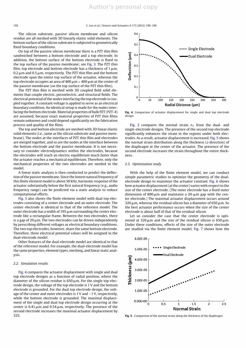
Fig. 4 compares the actuator displacement with single and dualtop electrode designs as a function of radial position, where thediameter of the silicon residue is 650 �m. For the single top elec-trode design, the voltage of the top electrode is 1 V and the bottomelectrode is grounded. For the dual top electrode design, the volt-age of the center and outer electrodes is 1 V and −1 V, respectively,while the bottom electrode is grounded. The maximal displace-ment of the single and dual top electrode design occurring at thecenter is 0.41 �m and 0.54 �m, respectively. The presence of thesecond electrode increases the maximal actuator displacement by32%.
Fig. 4. Comparison of actuator displacement for single and dual top electrodedesign.
Fig. 2 compares the normal strain �x from the dual- andsingle-electrode designs. The presence of the second top electrodesignificantly enhances the strain in the regions under both elec-trodes. As a result, actuator displacement is increased. Fig. 5 showsthe normal strain distribution along the thickness (z-direction) ofthe diaphragm at the center of the actuator. The presence of thesecond electrode increases the strain throughout the entire thick-ness.
2.3. Optimization study
With the help of the finite element model, we can conductsimple parametric studies to optimize the geometry of the dual-electrode design to maximize the actuator constant. Fig. 6 showshow actuator displacement (at the center) varies with respect to thesize of the center electrode. (The outer electrode has a fixed outerdimension of 800 �m and maintains a 20-�m gap with the cen-ter electrode.) The maximal actuator displacement occurs around320 �m, whereas the residual silicon has a diameter of 650 �m. Sothe best actuator performance occurs when the size of the centerelectrode is about half of that of the residual silicon.
Let us consider the case that the center electrode is opti-mized at 320 �m and the size of the residual silicon is 650 �m.Under these conditions, effects of the size of the outer electrodeare studied via the finite element model. Fig. 7 shows how the
Fig. 5. Comparison of the normal strain along the thickness of the diaphragm.
Author's personal copy
C. Luo et al. / Sensors and Actuators A 173 (2012) 190– 196 193
Fig. 6. Actuator displacement with respect to the seize of center electrode.
displacement at the actuator center varies with respect to the size ofthe outer electrode. The variation consists of three portions. Whenthe outer electrode exceeds 650 �m, the displacement saturatesaround 0.58 �m. As the outer electrode decreases in size, the dis-placement drops steadily and stabilizes at 0.4 �m. Since the sizeof the residual silicon is 650 �m, results from Fig. 7 imply that theouter electrode must overlap with the residual silicon to deliver themaximal actuator displacement.
3. Experimental verification
Calibrated experiments are conducted to verify the simulationresults. Specimen preparation, experimental setup and measure-ment results are described in detail as follows.
3.1. Specimen preparation
Fig. 8 illustrates the fabrication process using an improvedsol–gel process that employs rapid thermal annealing and a dilutesealant coating. The silicon substrate is first oxidized in a fur-nace at 1045 ◦C for 2 h to grow a SiO2 layer of 500 nm thick.Then a layer silicon nitride of 200 nm thick is deposited by PECVD(plasma enhanced chemical vapor deposition). The bottom elec-trode consists of Pt/Ti layers with thickness of 100 nm and 50 nm,
Fig. 7. Actuator displacement with respect to the size of the outer electrode.
Fig. 8. Preparation processes of actuators.
respectively (Fig. 8(a)). The PZT film is spin-coated three times.For the first two coatings, the sintering temperature is 650 ◦C for15 min. For the third coating, the sol is diluted 50% by acetic acidand sintering temperature is 450 ◦C for 10 min (Fig. 8(b) and (c)). Tofabricate the top electrodes, conducting layers consisting of Au/Crare deposited through evaporation (Fig. 8(d)). The dual top elec-trodes are patterned and formed through lift-off (Fig. 8(e)). Finally,the backside of the silicon is etched via deep reactive ion etch (DRIE)to form the diaphragm suspension (Fig. 8(f)).
Fig. 9 shows the top view of the fabricated actuator withdual top electrodes under an optical microscope. As one can see,the outer electrode does not completely enclose the center elec-trode, because space is needed for a connecting wire to reach thecenter electrode from outside. For the actuator shown in Fig. 9,the center electrode is 390 �m × 390 �m, and the width of theconnecting wire is 100 �m. In addition, the outer electrode is800 �m × 800 �m; therefore, it is the same size as the diaphragm.The circle in dash line refers to the boundary of the residual silicon,which is about 650 �m.
3.2. Experimental setup and results
The experiment setup consists of two function generators, alaser Doppler velocimetry (LDV), an oscilloscope, and an actuatorspecimen to be tested; see Fig. 10. The function generators drive thecenter and outer electrode, respectively. The excitations are sinu-soidal with a frequency of 3 kHz. Moreover, the phase differencebetween the two driving voltages is adjustable. The LDV measures
Fig. 9. Microscope picture of the actuator.
Author's personal copy
194 C. Luo et al. / Sensors and Actuators A 173 (2012) 190– 196
Fig. 10. Schematics of experiment setup.
out-of-plane velocity of the actuator specimen. The oscilloscoperecords the two input driving signals and the output LDV velocitymeasurement. In particular, channels 1 and 2 of the oscilloscoperepresent the driving signal for the center electrode and the outerelectrode, respectively. Channel 3 records the LDV velocity mea-surement.
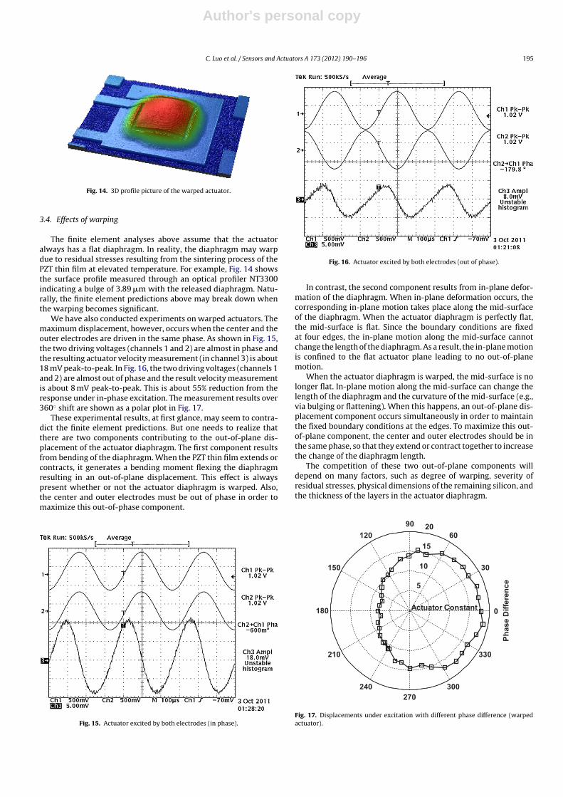
The measurements of actuator displacements under dual exci-tations with different phase differences are shown in Fig. 11 as apolar plot. The radial scale shows the measured actuator constantin nm/V, while the circumferential direction indicates the phasedifference of the dual excitations in degrees. The actuator displace-ment reaches its maximum of 17 nm/V when the phase differenceis 180◦. When the two electrodes are driven in the same phase, theactuator has a minimal displacement of 5 nm/V. A phase differenceof 90◦ generates a median displacement of about 12 nm/V. Theseresults are consistent with those predicted from the finite elementanalysis.
3.3. Applications to misaligned microactuators
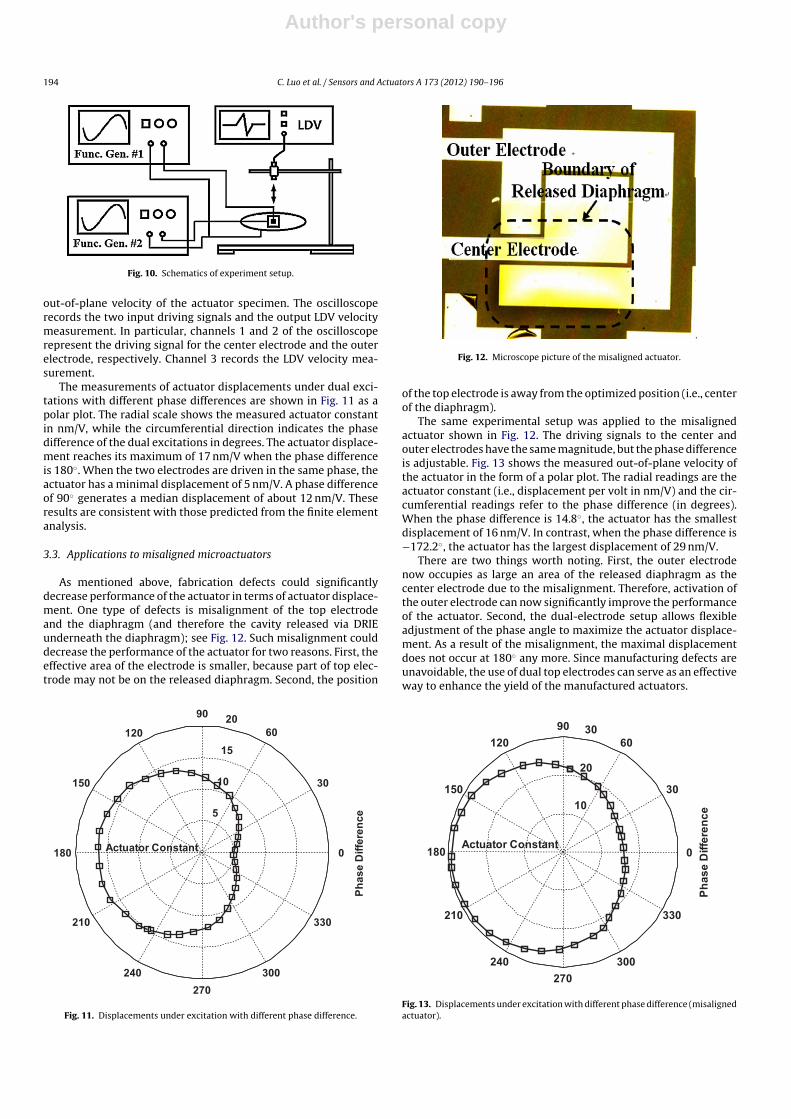
As mentioned above, fabrication defects could significantlydecrease performance of the actuator in terms of actuator displace-ment. One type of defects is misalignment of the top electrodeand the diaphragm (and therefore the cavity released via DRIEunderneath the diaphragm); see Fig. 12. Such misalignment coulddecrease the performance of the actuator for two reasons. First, theeffective area of the electrode is smaller, because part of top elec-trode may not be on the released diaphragm. Second, the position
5
10
15
20
30
210
60
240
90
270
120
300
150
330
0081Actuator Con stant
Ph
as
e D
iffe
re
nc
e
Fig. 11. Displacements under excitation with different phase difference.
Fig. 12. Microscope picture of the misaligned actuator.
of the top electrode is away from the optimized position (i.e., centerof the diaphragm).
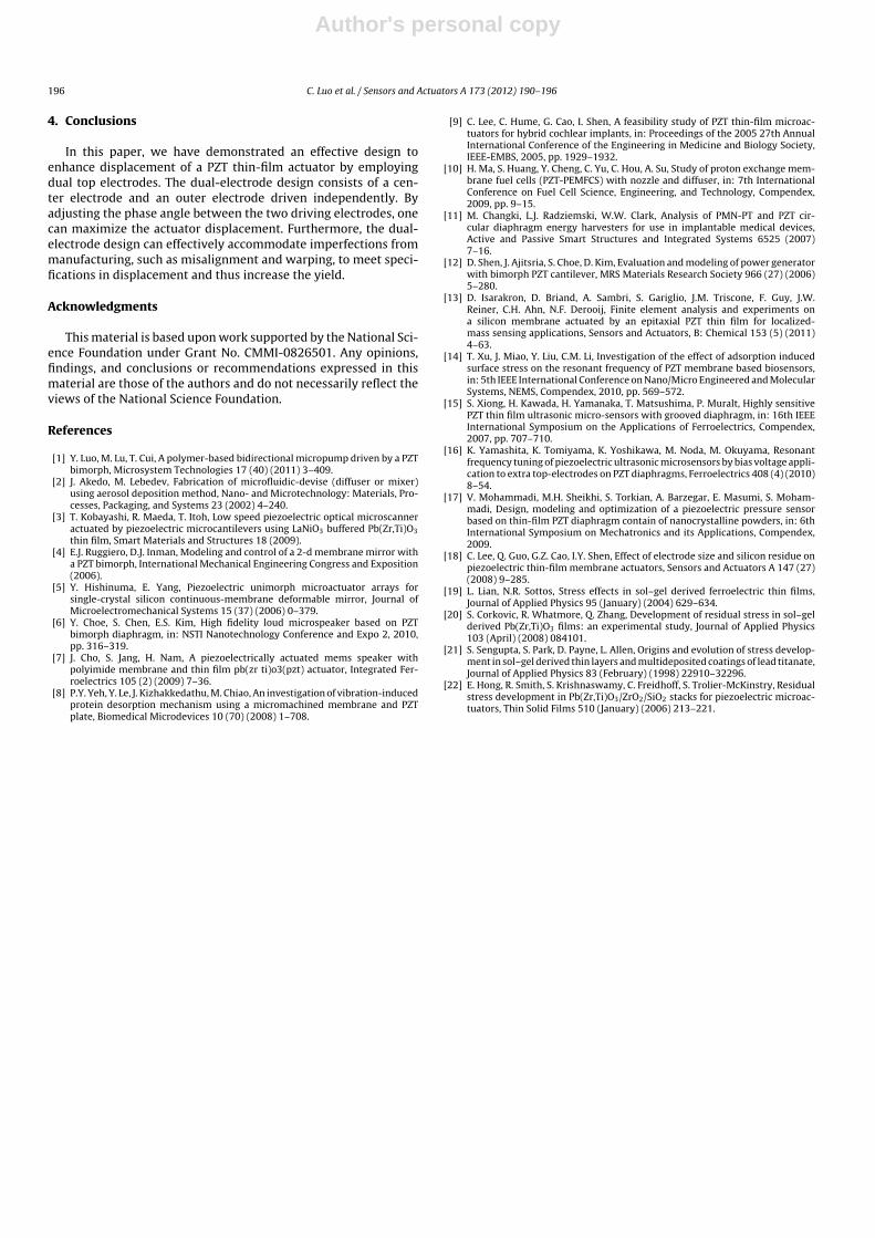
The same experimental setup was applied to the misalignedactuator shown in Fig. 12. The driving signals to the center andouter electrodes have the same magnitude, but the phase differenceis adjustable. Fig. 13 shows the measured out-of-plane velocity ofthe actuator in the form of a polar plot. The radial readings are theactuator constant (i.e., displacement per volt in nm/V) and the cir-cumferential readings refer to the phase difference (in degrees).When the phase difference is 14.8◦, the actuator has the smallestdisplacement of 16 nm/V. In contrast, when the phase difference is−172.2◦, the actuator has the largest displacement of 29 nm/V.
There are two things worth noting. First, the outer electrodenow occupies as large an area of the released diaphragm as thecenter electrode due to the misalignment. Therefore, activation ofthe outer electrode can now significantly improve the performanceof the actuator. Second, the dual-electrode setup allows flexibleadjustment of the phase angle to maximize the actuator displace-ment. As a result of the misalignment, the maximal displacementdoes not occur at 180◦ any more. Since manufacturing defects areunavoidable, the use of dual top electrodes can serve as an effectiveway to enhance the yield of the manufactured actuators.
10
20
30
30
210
60
240
90
270
120
300
150
330
180 0Actuator Con stant
Ph
as
e D
iffe
re
nc
e
Fig. 13. Displacements under excitation with different phase difference (misalignedactuator).
Author's personal copy
C. Luo et al. / Sensors and Actuators A 173 (2012) 190– 196 195
Fig. 14. 3D profile picture of the warped actuator.
3.4. Effects of warping
The finite element analyses above assume that the actuatoralways has a flat diaphragm. In reality, the diaphragm may warpdue to residual stresses resulting from the sintering process of thePZT thin film at elevated temperature. For example, Fig. 14 showsthe surface profile measured through an optical profiler NT3300indicating a bulge of 3.89 �m with the released diaphragm. Natu-rally, the finite element predictions above may break down whenthe warping becomes significant.
We have also conducted experiments on warped actuators. Themaximum displacement, however, occurs when the center and theouter electrodes are driven in the same phase. As shown in Fig. 15,the two driving voltages (channels 1 and 2) are almost in phase andthe resulting actuator velocity measurement (in channel 3) is about18 mV peak-to-peak. In Fig. 16, the two driving voltages (channels 1and 2) are almost out of phase and the result velocity measurementis about 8 mV peak-to-peak. This is about 55% reduction from theresponse under in-phase excitation. The measurement results over360◦ shift are shown as a polar plot in Fig. 17.
These experimental results, at first glance, may seem to contra-dict the finite element predictions. But one needs to realize thatthere are two components contributing to the out-of-plane dis-placement of the actuator diaphragm. The first component resultsfrom bending of the diaphragm. When the PZT thin film extends orcontracts, it generates a bending moment flexing the diaphragmresulting in an out-of-plane displacement. This effect is alwayspresent whether or not the actuator diaphragm is warped. Also,the center and outer electrodes must be out of phase in order tomaximize this out-of-phase component.
Fig. 15. Actuator excited by both electrodes (in phase).
Fig. 16. Actuator excited by both electrodes (out of phase).
In contrast, the second component results from in-plane defor-mation of the diaphragm. When in-plane deformation occurs, thecorresponding in-plane motion takes place along the mid-surfaceof the diaphragm. When the actuator diaphragm is perfectly flat,the mid-surface is flat. Since the boundary conditions are fixedat four edges, the in-plane motion along the mid-surface cannotchange the length of the diaphragm. As a result, the in-plane motionis confined to the flat actuator plane leading to no out-of-planemotion.
When the actuator diaphragm is warped, the mid-surface is nolonger flat. In-plane motion along the mid-surface can change thelength of the diaphragm and the curvature of the mid-surface (e.g.,via bulging or flattening). When this happens, an out-of-plane dis-placement component occurs simultaneously in order to maintainthe fixed boundary conditions at the edges. To maximize this out-of-plane component, the center and outer electrodes should be inthe same phase, so that they extend or contract together to increasethe change of the diaphragm length.
The competition of these two out-of-plane components willdepend on many factors, such as degree of warping, severity ofresidual stresses, physical dimensions of the remaining silicon, andthe thickness of the layers in the actuator diaphragm.
5
10
15
20
30
210
60
240
90
270
120
300
150
330
180 0Actuator Constant
Ph
as
e D
iffe
re
nc
e
Fig. 17. Displacements under excitation with different phase difference (warpedactuator).
Author's personal copy
196 C. Luo et al. / Sensors and Actuators A 173 (2012) 190– 196
4. Conclusions
In this paper, we have demonstrated an effective design toenhance displacement of a PZT thin-film actuator by employingdual top electrodes. The dual-electrode design consists of a cen-ter electrode and an outer electrode driven independently. Byadjusting the phase angle between the two driving electrodes, onecan maximize the actuator displacement. Furthermore, the dual-electrode design can effectively accommodate imperfections frommanufacturing, such as misalignment and warping, to meet speci-fications in displacement and thus increase the yield.
Acknowledgments
This material is based upon work supported by the National Sci-ence Foundation under Grant No. CMMI-0826501. Any opinions,findings, and conclusions or recommendations expressed in thismaterial are those of the authors and do not necessarily reflect theviews of the National Science Foundation.
References
[1] Y. Luo, M. Lu, T. Cui, A polymer-based bidirectional micropump driven by a PZTbimorph, Microsystem Technologies 17 (40) (2011) 3–409.
[2] J. Akedo, M. Lebedev, Fabrication of microfluidic-devise (diffuser or mixer)using aerosol deposition method, Nano- and Microtechnology: Materials, Pro-cesses, Packaging, and Systems 23 (2002) 4–240.
[3] T. Kobayashi, R. Maeda, T. Itoh, Low speed piezoelectric optical microscanneractuated by piezoelectric microcantilevers using LaNiO3 buffered Pb(Zr,Ti)O3
thin film, Smart Materials and Structures 18 (2009).[4] E.J. Ruggiero, D.J. Inman, Modeling and control of a 2-d membrane mirror with
a PZT bimorph, International Mechanical Engineering Congress and Exposition(2006).
[5] Y. Hishinuma, E. Yang, Piezoelectric unimorph microactuator arrays forsingle-crystal silicon continuous-membrane deformable mirror, Journal ofMicroelectromechanical Systems 15 (37) (2006) 0–379.
[6] Y. Choe, S. Chen, E.S. Kim, High fidelity loud microspeaker based on PZTbimorph diaphragm, in: NSTI Nanotechnology Conference and Expo 2, 2010,pp. 316–319.
[7] J. Cho, S. Jang, H. Nam, A piezoelectrically actuated mems speaker withpolyimide membrane and thin film pb(zr ti)o3(pzt) actuator, Integrated Fer-roelectrics 105 (2) (2009) 7–36.
[8] P.Y. Yeh, Y. Le, J. Kizhakkedathu, M. Chiao, An investigation of vibration-inducedprotein desorption mechanism using a micromachined membrane and PZTplate, Biomedical Microdevices 10 (70) (2008) 1–708.
[9] C. Lee, C. Hume, G. Cao, I. Shen, A feasibility study of PZT thin-film microac-tuators for hybrid cochlear implants, in: Proceedings of the 2005 27th AnnualInternational Conference of the Engineering in Medicine and Biology Society,IEEE-EMBS, 2005, pp. 1929–1932.
[10] H. Ma, S. Huang, Y. Cheng, C. Yu, C. Hou, A. Su, Study of proton exchange mem-brane fuel cells (PZT-PEMFCS) with nozzle and diffuser, in: 7th InternationalConference on Fuel Cell Science, Engineering, and Technology, Compendex,2009, pp. 9–15.
[11] M. Changki, L.J. Radziemski, W.W. Clark, Analysis of PMN-PT and PZT cir-cular diaphragm energy harvesters for use in implantable medical devices,Active and Passive Smart Structures and Integrated Systems 6525 (2007)7–16.
[12] D. Shen, J. Ajitsria, S. Choe, D. Kim, Evaluation and modeling of power generatorwith bimorph PZT cantilever, MRS Materials Research Society 966 (27) (2006)5–280.
[13] D. Isarakron, D. Briand, A. Sambri, S. Gariglio, J.M. Triscone, F. Guy, J.W.Reiner, C.H. Ahn, N.F. Derooij, Finite element analysis and experiments ona silicon membrane actuated by an epitaxial PZT thin film for localized-mass sensing applications, Sensors and Actuators, B: Chemical 153 (5) (2011)4–63.
[14] T. Xu, J. Miao, Y. Liu, C.M. Li, Investigation of the effect of adsorption inducedsurface stress on the resonant frequency of PZT membrane based biosensors,in: 5th IEEE International Conference on Nano/Micro Engineered and MolecularSystems, NEMS, Compendex, 2010, pp. 569–572.
[15] S. Xiong, H. Kawada, H. Yamanaka, T. Matsushima, P. Muralt, Highly sensitivePZT thin film ultrasonic micro-sensors with grooved diaphragm, in: 16th IEEEInternational Symposium on the Applications of Ferroelectrics, Compendex,2007, pp. 707–710.
[16] K. Yamashita, K. Tomiyama, K. Yoshikawa, M. Noda, M. Okuyama, Resonantfrequency tuning of piezoelectric ultrasonic microsensors by bias voltage appli-cation to extra top-electrodes on PZT diaphragms, Ferroelectrics 408 (4) (2010)8–54.
[17] V. Mohammadi, M.H. Sheikhi, S. Torkian, A. Barzegar, E. Masumi, S. Moham-madi, Design, modeling and optimization of a piezoelectric pressure sensorbased on thin-film PZT diaphragm contain of nanocrystalline powders, in: 6thInternational Symposium on Mechatronics and its Applications, Compendex,2009.
[18] C. Lee, Q. Guo, G.Z. Cao, I.Y. Shen, Effect of electrode size and silicon residue onpiezoelectric thin-film membrane actuators, Sensors and Actuators A 147 (27)(2008) 9–285.
[19] L. Lian, N.R. Sottos, Stress effects in sol–gel derived ferroelectric thin films,Journal of Applied Physics 95 (January) (2004) 629–634.
[20] S. Corkovic, R. Whatmore, Q. Zhang, Development of residual stress in sol–gelderived Pb(Zr,Ti)O3 films: an experimental study, Journal of Applied Physics103 (April) (2008) 084101.
[21] S. Sengupta, S. Park, D. Payne, L. Allen, Origins and evolution of stress develop-ment in sol–gel derived thin layers and multideposited coatings of lead titanate,Journal of Applied Physics 83 (February) (1998) 22910–32296.
[22] E. Hong, R. Smith, S. Krishnaswamy, C. Freidhoff, S. Trolier-McKinstry, Residualstress development in Pb(Zr,Ti)O3/ZrO2/SiO2 stacks for piezoelectric microac-tuators, Thin Solid Films 510 (January) (2006) 213–221.