Page 1
www.studymafia.org
A
Seminar report
On
Automatic Gate Alarm with Light
Submitted in partial fulfillment of the requirement for the award of degree
Of Mechanical
SUBMITTED TO: SUBMITTED BY: www.studymafia.org www.studymafia.org
Page 2
www.studymafia.org
Preface
I have made this report file on the topic Automatic Gate Alarm with Light; I have tried my
best to elucidate all the relevant detail to the topic to be included in the report. While in the
beginning I have tried to give a general view about this topic.
My efforts and wholehearted co-corporation of each and everyone has ended on a successful
note. I express my sincere gratitude to …………..who assisting me throughout the preparation
of this topic. I thank him for providing me the reinforcement, confidence and most importantly
the track for the topic whenever I needed it.
Page 3
www.studymafia.org
Acknowledgement
I would like to thank respected Mr…….. and Mr. ……..for giving me such a wonderful
opportunity to expand my knowledge for my own branch and giving me guidelines to present a
seminar report. It helped me a lot to realize of what we study for.
Secondly, I would like to thank my parents who patiently helped me as i went through my work
and helped to modify and eliminate some of the irrelevant or un-necessary stuffs.
Thirdly, I would like to thank my friends who helped me to make my work more organized and
well-stacked till the end.
Next, I would thank Microsoft for developing such a wonderful tool like MS Word. It helped
my work a lot to remain error-free.
Last but clearly not the least, I would thank The Almighty for giving me strength to complete
my report on time.
Page 4
www.studymafia.org
Content
INTRODUCTION
MOTIVATION
PRINCIPLE
MONOSTABLE MULTIVIBRATOR
ASTABLE MULTIVIBRATOR
TSOP
LDR
RELAY AND FREE WHEELING DIODE
CIRCUIT DIAGRAM
WORKING
ADVANTAGES
CONCLUSION
Page 5
www.studymafia.org
INTRODUCTION
Burglary of residences, retail establishments, and other commercial facilities involves
breaking and entering, and stealing property. Attempted forcible entry into a property is also
classified as burglary, in the FBI's Uniform Crime Reports (UCR) definition.
As of 1999, there were 1.4 million residential burglaries reported in the United States,
which was a record low number, not seen since 1966.[9] Though, up to 50% of burglaries are not
reported to the police
PIRs verify if an intruder or object is actually there. Creating individual zones of
detection where each zone comprises one or more layers can achieve differentiation. Between the
zones there are areas of no sensitivity (dead zones) that are used by the sensor for comparison.
The circuit may be used to automatically switch on a light at the entrance gate to the
premises at night by sensing the presence of a person. In addition, it sounds an alarm to signify
the presence of a person. Here we are using an IR Led as the transmitting unit and the TSOP as
receiving unit. A monostable, multivibrator circuit is used for the purpose of getting time delay
accordingly. Lamp is switched on only for a short interval to save electricity. The main
application is its use in restricted areas to indicate the entry of trespassers. It can also be used for
security purposes.
Page 6
www.studymafia.org
MOTIVATION
In the present busy world cases may arise where we may not be able to keep a constant
watch in certain areas. In such cases arises the application of our project. This actually serves as
a detecting mechanism to indicate the presence of an object or person in undetected cases. This
turned out to be our main motivation for us to do this project.
The necessity to find a solution of all these problems turned out to be the
motivation; also we have succeeded in overcoming these difficulties by implementing this
project.
Page 7
www.studymafia.org
PRINCIPLE
This circuit has two stages: Transmitting unit and receiving unit. Transmitting unit
consists of IR LED and sensing unit consists of TSOP sensor. An IC 555 working in monostable
mode gives the time delay. The circuit may be used to automatically switch on a light at the
entrance gate to the premises at night by sensing the presence of a person. In addition, it sounds
an alarm to signify the presence of a person. Here we are using an IR Led as the transmitting unit
and the TSOP as receiving unit. A monostable, multivibrator circuit is used for the purpose of
getting time delay accordingly. Monostable multivibrator often called a one shot multivibrator is
a pulse generating circuit in which the duration of this pulse is determined by the RC network
connected externally to the 555 timer. In a stable or standby state, the output of the circuit is
approximately zero or a logic-low level. When external trigger pulse is applied output is forced
to go high (» VCC). The monostable circuit has only one stable state (output low) hence the name
monostable. Astable Multivibrator is a two stage switching circuit in which the output of the first
stage is fed to the input of the second stage and vice versa. The outputs of both the stages are
complementary. This free running multivibrator generates square wave without any external
triggering pulse. The circuit has two stable states and switches back and forth from one state to
another, remaining in each state for a time depending upon the discharging of the capacitive
circuit. Lamp is switched on only for a short interval to save electricity. An LDR based circuit is
used to switch on the bulb at night only. The buzzer is connected such that it functions whenever
the IR beam is interrupted.
Page 8
www.studymafia.org
MONOSTABLE MULTIVIBRATOR
Monostable multivibrator often called a one shot multivibrator is a pulse generating
circuit in which the duration of this pulse is determined by the RC network connected externally
to the 555 timer. In a stable or standby state, the output of the circuit is approximately zero or a
logic- VCC). The
time for which output remains high is determined by the external RC network connected to the
timer. At the end of the timing interval, the output automatically reverts back to its logic-low
stable state. The output stays low until trigger pulse is again applied. Then the cycle repeats. The
monostable circuit has only one stable state (output low) hence the name monostable.
Operation:
Initially when the circuit is in the stable state i.e. when the output is low, transistor Q1 is
ON and the capacitor C is shorted out to ground. Upon the application of a negative trigger pulse
to pin 2, transistor Q1 is turned OFF, which releases the short circuit across the external
capacitor C and drives the output high. The capacitor C now starts charging up towards VCC
through R. When the voltage across the capacitor equals 2/3 VCC, comparator 1’s output switches
from low to high, which in turn drives the output to its low state via the output of the flip-flop. At
the same time the output of the flip-flop turns transistor Q1 ON and hence the capacitor C
rapidly discharges through the transistor. The output of the monostable remains low until a
trigger pulse is again applied. Then the cycle repeats. The pulse width of the trigger input must
Page 9
www.studymafia.org
be smaller than the expected pulse width of the output waveform. Also the trigger pulse must be
a negative going input signal with amplitude larger than 1/3 VCC.
Once triggered, the circuit’s output will remain in the high state until the set time, t
elapses. The output will not change its state even if an input trigger is applied again during this
time interval t. The circuit can be reset during the timing cycle by applying negative pulse to the
reset terminal. The output will remain in the low state until a trigger is again applied.
Pin1: Ground. All voltages are measured w.r.t this terminal.
Pin2: Trigger. The output of the timer depends on the amplitude of the external trigger pulse
applied to this pin. The output is low if the voltage at this pin is greater than 2/3 VCC. When a
negative going pulse of amplitude greater than 1/3 VCC is applied to this pin, comparator 2 output
goes low, which in turn switches the output of the timer high. The output remains high as long as
the trigger terminal is held at a low voltage.
Pin3: Output. There are two ways by which a load can be connected to the output terminal:
either between pin 3 and ground or between pin3 and supply voltage +VCC. When the output is
low the load current flows through the load connected between pin3 and +VCC into the output
terminal and is called sink current. The current through the grounded load is zero when the
output is low. For this reason the load connected between pin 3 and +VCC is called the normally
on load and that connected between pin 3 and ground is called normally off-load. On the other
hand, when the output is high the current through the load connected between pin 3 and +VCC is
zero. The output terminal supplies current to the normally off load. This current is called source
current
Pin4: Reset. The 555 timer can be reset (disabled) by applying a negative pulse to this pin. When
the reset function is not in use, the reset terminal should be connected to +VCC to avoid any
possibility of false triggering.
Pin5: Control Voltage. An external voltage applied to this terminal changes the threshold as well
as trigger voltage. Thus by imposing a voltage on this pin or by connecting a pot between this
pin and ground, the pulse width of the output waveform can be varied.
Page 10
www.studymafia.org
Pin6: Threshold. This is the non-inverting input of comparator 1, which monitors the voltage
across the external capacitor. When the voltage at this pin is greater than or equal to the threshold
voltage 2/3 VCC, the output of comparator 1 goes high, which in turn switches the output of the
timer low.
Pin7: Discharge. This pin is connected internally to the collector of transistor Q1. When the
output is high Q1 is OFF and acts as an open circuit to external capacitor C connected across it.
On the other hand, when the output is low, Q1 is saturated and acts as a short circuit, shorting out
the external capacitor C to ground.
Pin8: +VCC. The supply voltage of +5V to + 18V is applied to this pin with respect to ground.
Page 11
www.studymafia.org
ASTABLE MULTIVIBRATOR
Astable Multivibrator is a two stage switching circuit in which the output of the first
stage is fed to the input of the second stage and vice versa. The outputs of both the stages are
complementary. This free running multivibrator generates square wave without any external
triggering pulse. The circuit has two stable states and switches back and forth from one state to
another, remaining in each state for a time depending upon the discharging of the capacitive
circuit
.
The multivibrator is one form of relaxation oscillator, the frequency of which may be
controlled by external synchronizing pulses. When supply voltage, VCC is applied, one transistor
will conduct more than the other due to some circuit imbalance. Initially let us assume that Q1 is
conducting and Q2 is cut-off. Then VC1, the output of Q1 is equal to VCESAT which is
approximately zero and VC2 is equal to VCC. At this instant C1 charges exponentially with the
time constant R1C1 towards the supply voltage through R1 and correspondingly VB2 also
increases exponentially towards VCC. When VB2 crosses the coupling voltage Q2 starts
conducting and VC2 falls to VCESAT. Also VB1 falls due to capacitive coupling between collector
of Q2 and base of Q1, thereby driving Q1 into OFF state. The rise in voltage VC1 is coupled
through C1 to the base of Q2 causing a small overshoot in voltage VB2. Thus Q1 is OFF and Q2
is ON. At this instant the voltage levels are:
Page 12
www.studymafia.org
VB1 is negative, VC1=VCC, VB2=VBESAT and VC2=VCESAT.
When Q1 is OFF and Q2 is ON the voltage VB1 increases exponentially with a time
constant R2C2 towards VCC. Therefore Q1 is driven to saturation and Q2 to cut-off. Now the
voltage levels are:
VB1=VBESAT, VC1=VCESAT, VB2 is negative and VC2=VCC.
From the above it is clear that when Q2 is ON the falling voltage VC2 permits the
discharging of capacitor C2 which in turn drives Q1 into cut-off. The rising voltage of VC1 is fed
back to the base of Q2 tending to turn it ON. This process is regenerative.
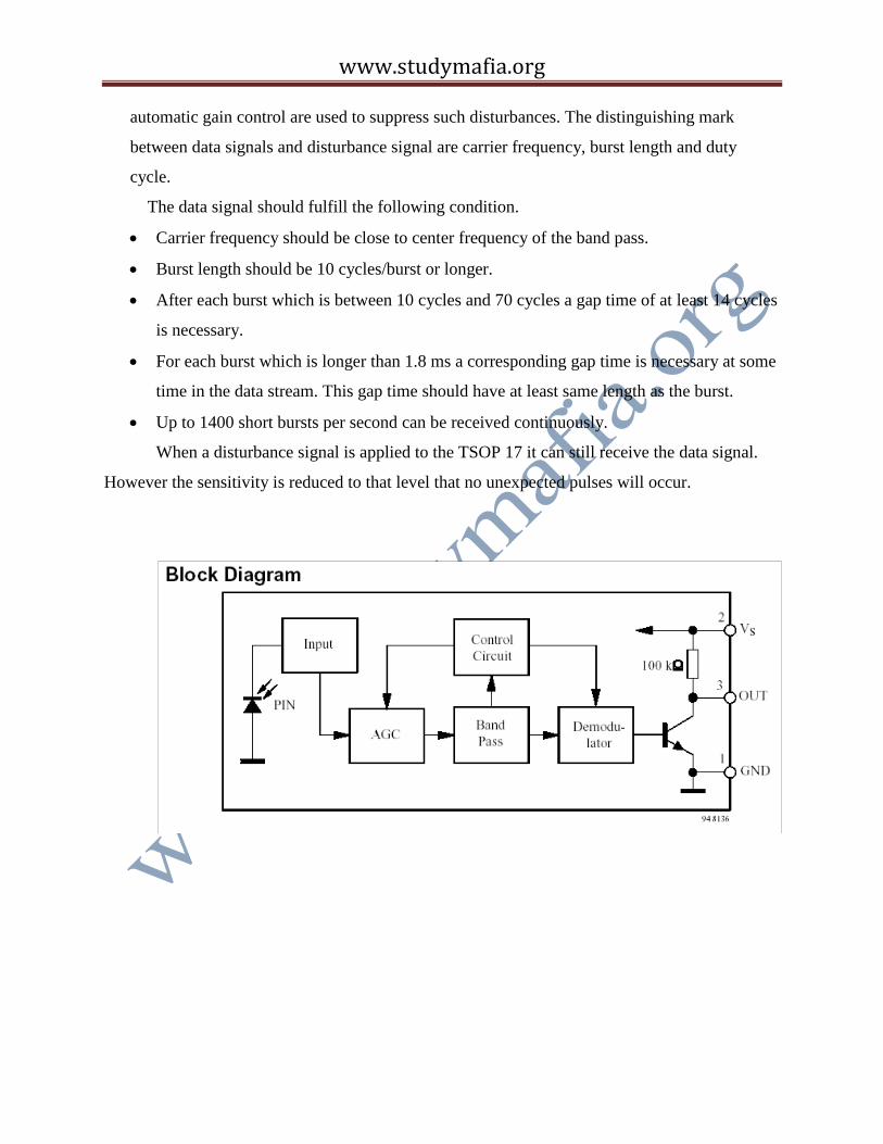
TSOP
The TSOP17 series are miniaturized receivers for infrared remote control systems. The
three pin terminals of the TSOP are GND, VCC and OUTPUT. The circuit of the TSOP17 is
designed in that way unexpected output pulses due to noise or disturbance signals are
avoided. A bandpassfilter and an integrator stage are used to suppress such disturbances.
FEATURES
Photo detector and pre amplifier in one package
Internal filter for PCM frequency
Improved shielding against electrical field disturbance
TTL, CMOS compatibility
Output active low
Low power consumption
High immunity against ambient light
Continuous data transmission possible
Suitable burst length >=10 cycles/burst
The circuit of the TSOP is designed in such a way that the unexpected output pulses due to
noise or disturbance signals are avoided. A band pass filter, an integrator stage and an
Page 13
www.studymafia.org
automatic gain control are used to suppress such disturbances. The distinguishing mark
between data signals and disturbance signal are carrier frequency, burst length and duty
cycle.
The data signal should fulfill the following condition.
Carrier frequency should be close to center frequency of the band pass.
Burst length should be 10 cycles/burst or longer.
After each burst which is between 10 cycles and 70 cycles a gap time of at least 14 cycles
is necessary.
For each burst which is longer than 1.8 ms a corresponding gap time is necessary at some
time in the data stream. This gap time should have at least same length as the burst.
Up to 1400 short bursts per second can be received continuously.
When a disturbance signal is applied to the TSOP 17 it can still receive the data signal.
However the sensitivity is reduced to that level that no unexpected pulses will occur.
Page 14
www.studymafia.org
LDR (LIGHT DEPENDENT RESISTOR)
A light-dependent resistor alternatively called an LDR, photoresistor, photoconductor, or
photocell, is a variable resistor whose value decreases with increasing incident light intensity.
An LDR is made of a high-resistance semiconductor. If light falling on the device is of
high enough frequency, photons absorbed by the semiconductor give bound electrons enough
energy to jump into the conduction band. The resulting free electron (and its hole partner)
conduct electricity, thereby lowering resistance.
A photoelectric device can be either intrinsic or extrinsic. In intrinsic devices, the only
available electrons are in the valence band, and hence the photon must have enough energy to
excite the electron across the entire band gap. Extrinsic devices have impurities added, which
have a ground state energy closer to the conduction band - since the electrons don't have as far to
jump, lower energy photons (i.e. longer wavelengths and lower frequencies) are sufficient to
trigger the device.
Two of its earliest applications were as part of smoke and fire detection systems and
camera light meters. Because cadmium sulfide cells are inexpensive and widely available, LDRs
are still used in electronic devices that need light detection capability, such as security alarms,
street lamps, and clock radios. The internal components of a photoelectric control for a typical
American streetlight. The photoresistor is facing rightwards, and controls whether current flows
through the heater which opens the main power contacts. At night, the heater cools, closing the
power contacts, energizing the street light. The heater/bimetal mechanism provides a built-in
time-delay.
A photoresistor is an electronic component whose resistance decreases with increasing
incident light intensity. It can also be referred to as a light-dependent resistor (LDR),
photoconductor, or photocell. A photoresistor is made of a high-resistance semiconductor. If
light falling on the device is of high enough frequency, photons absorbed by the semiconductor
give bound electrons enough energy to jump into the conduction band. The resulting free
Page 15
www.studymafia.org
electron (and its hole partner) conduct electricity, thereby lowering resistance. The circuit
symbol of LDR.
A photoelectric device can be either intrinsic or extrinsic. An intrinsic semiconductor has
its own charge carriers and is not an efficient semiconductor, e.g. silicon. In intrinsic devices, the
only available electrons are in the valence band, and hence the photon must have enough energy
to excite the electron across the entire band gap. Extrinsic devices have impurities added, which
have a ground state energy closer to the conduction band — since the electrons don't have as far
to jump, lower energy photons (i.e. longer wavelengths and lower frequencies) are sufficient to
trigger the device. If a sample of silicon has some of its atoms replaced by phosphorus atoms
(impurities), there will be extra electrons available for conduction. This is an example of an
extrinsic semiconductor. Cadmium sulphide or cadmium sulphide (CdS) cells rely on the
material's ability to vary its resistance according to the amount of light striking the cell. The
more light that strikes the cell, the lower the resistance. Although not accurate, even a simple
CdS cell can have a wide range of resistance from less than 100 Ω in bright light to in excess of
10 MΩ in darkness. Many commercially available CdS cells have a peak sensitivity in the region
of 500nm - 600nm. The cells are also capable of reacting to a broad range of frequencies,
including infrared (IR), visible light, and ultraviolet (UV). They are often found on street lights
as automatic on/off switches. They were once even used in heat-seeking missiles to sense for
targets.
Page 16
www.studymafia.org
APPLICATIONS
Photoresistors come in many different types. Inexpensive cadmium sulphide cells can be
found in many consumer items such as camera light meters, clock radios, security alarms, street
lights and outdoor clocks. They are also used in some dynamic compressors to control gain
reduction. At the other end of the scale, Ge:Cu photoconductors are among the best far-infrared
detectors available, and are used for infrared astronomy and infrared spectroscopy.
RELAY & FREE WHEELING DIODE
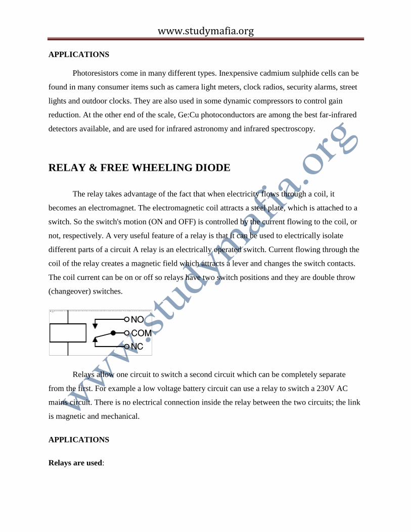
The relay takes advantage of the fact that when electricity flows through a coil, it
becomes an electromagnet. The electromagnetic coil attracts a steel plate, which is attached to a
switch. So the switch's motion (ON and OFF) is controlled by the current flowing to the coil, or
not, respectively. A very useful feature of a relay is that it can be used to electrically isolate
different parts of a circuit A relay is an electrically operated switch. Current flowing through the
coil of the relay creates a magnetic field which attracts a lever and changes the switch contacts.
The coil current can be on or off so relays have two switch positions and they are double throw
(changeover) switches.
Relays allow one circuit to switch a second circuit which can be completely separate
from the first. For example a low voltage battery circuit can use a relay to switch a 230V AC
mains circuit. There is no electrical connection inside the relay between the two circuits; the link
is magnetic and mechanical.
APPLICATIONS
Relays are used:
Page 17
www.studymafia.org
To control a high-current circuit with a low-current signal, as in the starter solenoid of an
automobile,
To control a high-voltage circuit with a low-voltage signal, as in some types of modems,
To detect and isolate faults on transmission and distribution lines by opening and closing
circuit breakers (protection relays),
To isolate the controlling circuit from the controlled circuit when the two are at different
potentials, for example when controlling a mains-powered device from a low-voltage
switch. The latter is often applied to control office lighting as the low voltage wires are
easily installed in partitions, which may be often moved as needs change. They may also
be controlled by room occupancy detectors in an effort to conserve energy,
To perform logic functions. For example, the boolean AND function is realised by
connecting NO relay contacts in series, the OR function by connecting NO contacts in
parallel. The change-over or Form C contacts perform the XOR (exclusive or) function.
Similar functions for NAND and NOR are accomplished using NC contacts. Due to the
failure modes of a relay compared with a semiconductor, they are widely used in safety
critical logic, such as the control panels of radioactive waste handling machinery.
To perform time delay functions. Relays can be modified to delay opening or delay
closing a set of contacts. A very short (a fraction of a second) delay would use a copper
disk between the armature and moving blade assembly. Current flowing in the disk
maintains magnetic field for a short time, lengthening release time. For a slightly longer
(up to a minute) delay, a dashpot is used. A dashpot is a piston filled with fluid that is
allowed to escape slowly. The time period can be varied by increasing or decreasing the
flow rate. For longer time periods, a mechanical clockwork timer is installed.
Page 18
www.studymafia.org
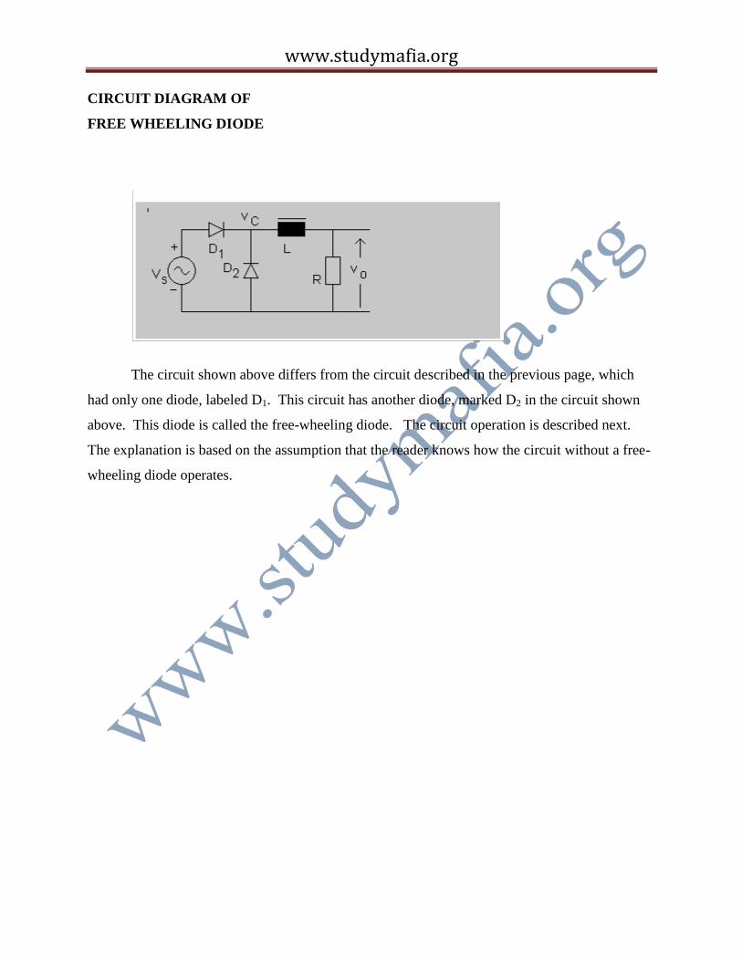
CIRCUIT DIAGRAM OF
FREE WHEELING DIODE
The circuit shown above differs from the circuit described in the previous page, which
had only one diode, labeled D1. This circuit has another diode, marked D2 in the circuit shown
above. This diode is called the free-wheeling diode. The circuit operation is described next.
The explanation is based on the assumption that the reader knows how the circuit without a free-
wheeling diode operates.
Page 19
www.studymafia.org
CIRCUIT OPERATION
Let the source voltage vs be defined to be E*sin (wt). The source voltage is positive
radians. When vs is positive,
diode D1 conducts and the voltage vc is positive. This in turn leads to diode D2 being reverse-
biased during this period. c would be negative if diode D1
tends to conduct. This means that D2 would be forward-biased and would conduct. When diode
D2 conducts, the voltage vc would be zero volts, assuming that the diode drop is negligible.
Additionally when diode D2 conducts, diode D1 remains reverse-biased, because the voltage vs. is
negative.
When the current through the inductor tends to fall, it starts acting as a source. When the
inductor acts as a source, its voltage tends to forward bias diode D2 if the source voltage vs is
negative and forward bias diode D1 if the source voltage vs is positive. Even when the source
voltage vs is positive, the inductor current would tend to fall if the source voltage is less than the
voltage drop across the load resistor.
During the negative half-cycle of source voltage, diode D1 blocks conduction and diode
D2 is forced to conduct. Since diode D2 allows the inductor current circulate through L, R and
D2, diode D2 is called the free-wheeling diode. We can say that the current free-wheels through
D2.
Page 20
www.studymafia.org
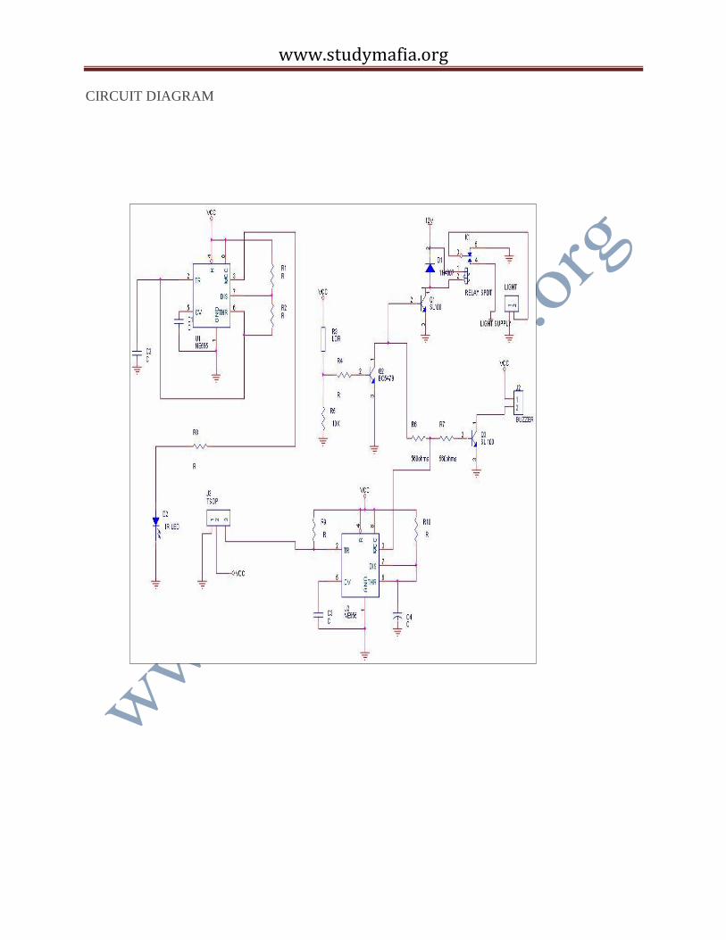
CIRCUIT DIAGRAM
Page 21
www.studymafia.org
WORKING
The astable multivibrator generates square wave of a particular frequency which is given
as input to IR LED. The LED generates IR rays which are received by the TSOP receiver.
When the IR rays get interrupted, a low output will be produced at the output terminal of
TSOP. This is given as a trigger to the monostable MVB which in turn produces a high
output. This high output is fed to the base of Q3 which pulls it to ground. The ground voltage
comes to one of the two terminals of the buzzer and supply voltage is given to its other
terminal. Thus the buzzer functions and indicates the presence of a person.
During night, when no light falls on LDR, it has high resistance. So low voltage comes in
the base of Q2 and it goes OFF. This results in a high voltage at the base of Q1 and it is
pulled to ground. So the relay is de-energized and this shifts the switch contact from position
5 to 4.Thus supply voltage comes to one terminal of bulb whose other terminal is grounded
and the bulb is switched on. During daytime when light falls on LDR its resistance goes low.
So high voltage comes to the base of Q2 which turns it ON and it is pulled to ground.
This ground voltage is fed to the base of Q1 and it turns OFF. The relay is energized and the
contact is switched back to 5.Thus the bulb circuit is incomplete and the bulb switches off.
Page 22
www.studymafia.org
ADVANTAGES
High sensitivity
Low cost
Simple construction
Easy to install and maintain
Less power consuming
Requires less space
Reliable
Page 23
www.studymafia.org
CONCLUSION
The project provides the detecting mechanism of objects or person at unexpected timings.
The project is user-friendly and highly reliable. This project has the advantage of saving of
electricity since the bulb glows in the dark only for a short interval of time. Another main
advantage which we could point out is the height adjusting mechanism which we could
implement.
With the use of high intensity alarms this can also be used for security purposes. Thus it
turns out to be a domestic as well as security purpose project. System reliability can be a problem
when it causes nuisance alarms, false alarms, or fails to alarm when called for. Nuisance alarms
occur when an unintended event evokes an alarm status by an otherwise properly working alarm
system or when there is an alarm system malfunction that results in an alarm state. It is easier to
know when there are false alarms, because the system is designed to react to that condition.
Failure alarms are more troublesome because they usually require periodic testing to make sure
the sensors are working and that the correct signals are getting through to the monitor. Some
systems are designed to detect problems internally, such as low or dead batteries, loose
connections, phone circuit trouble, etc. While earlier nuisance alarms could be set off by small
disturbances, like insects or pets, newer model alarms have technology to measure the
size/weight of the object causing the disturbance, and thus are able to decide how serious the
threat is, which is especially useful in burglar alarms.
Home and business owners can now choose a new type of keypad control panel designed
to help reduce false alarms.
Based on a standard called CP-01-2000, developed by the American National Standards
Institute (ANSI)[1] and Security Industry Association (SIA))[2] , the new generation of keypad
control panels takes aim at user error by building in extra precautions that minimize unwarranted
dispatch of emergency responders.
Page 24
www.studymafia.org
Some of the features of CP-01 keypads include a progress annunciation function that
emits a different sound during the last 10 seconds of delay, which hastens exit from the premises.
Also, the exit time doubles if the user disables the pre-warning feature.
Page 25
www.studymafia.org
References
www.google.com
www.wikipedia.com
www.studymafia.org