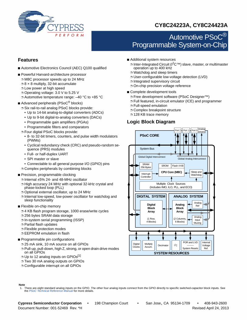
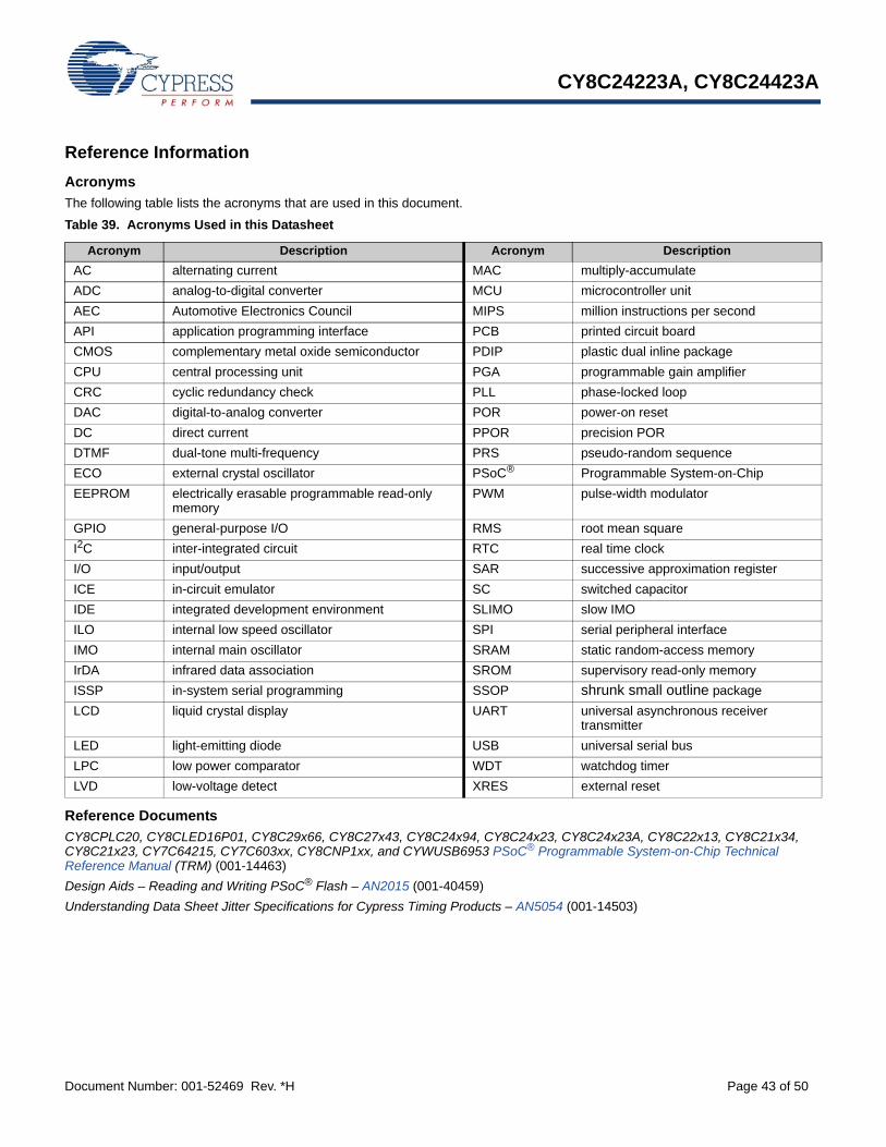
CY8C24223A, CY8C24423A Automotive PSoC ® Programmable System-on-Chip Cypress Semiconductor Corporation • 198 Champion Court • San Jose, CA 95134-1709 • 408-943-2600 Document Number: 001-52469 Rev. *H Revised April 24, 2013 Features ■ Automotive Electronics Council (AEC) Q100 qualified ■ Powerful Harvard-architecture processor ❐ M8C processor speeds up to 24 MHz ❐ 8 × 8 multiply, 32-bit accumulate ❐ Low power at high speed ❐ Operating voltage: 3.0 V to 5.25 V ❐ Automotive temperature range: –40 °C to +85 °C ■ Advanced peripherals (PSoC ® blocks) ❐ Six rail-to-rail analog PSoC blocks provide: • Up to 14-bit analog-to-digital converters (ADCs) • Up to 9-bit digital-to-analog converters (DACs) • Programmable gain amplifiers (PGAs) • Programmable filters and comparators ❐ Four digital PSoC blocks provide: • 8- to 32-bit timers, counters, and pulse width modulators (PWMs) • Cyclical redundancy check (CRC) and pseudo-random se- quence (PRS) modules • Full- or half-duplex UART • SPI master or slave • Connectable to all general purpose I/O (GPIO) pins ❐ Complex peripherals by combining blocks ■ Precision, programmable clocking ❐ Internal ±5% 24- and 48-MHz oscillator ❐ High accuracy 24 MHz with optional 32-kHz crystal and phase-locked loop (PLL) ❐ Optional external oscillator, up to 24 MHz ❐ Internal low-speed, low-power oscillator for watchdog and sleep functionality ■ Flexible on-chip memory ❐ 4 KB flash program storage, 1000 erase/write cycles ❐ 256 bytes SRAM data storage ❐ In-system serial programming (ISSP) ❐ Partial flash updates ❐ Flexible protection modes ❐ EEPROM emulation in flash ■ Programmable pin configurations ❐ 25 mA sink, 10 mA source on all GPIOs ❐ Pull-up, pull-down, high Z, strong, or open drain drive modes on all GPIOs ❐ Up to 12 analog inputs on GPIOs [1] ❐ Two 30 mA analog outputs on GPIOs ❐ Configurable interrupt on all GPIOs ■ Additional system resources ❐ Inter-Integrated Circuit (I 2 C™) slave, master, or multimaster operation up to 400 kHz ❐ Watchdog and sleep timers ❐ User-configurable low-voltage detection (LVD) ❐ Integrated supervisory circuit ❐ On-chip precision voltage reference ■ Complete development tools ❐ Free development software (PSoC Designer™) ❐ Full featured, in-circuit emulator (ICE) and programmer ❐ Full-speed emulation ❐ Complex breakpoint structure ❐ 128 KB trace memory Logic Block Diagram Note 1. There are eight standard analog inputs on the GPIO. The other four analog inputs connect from the GPIO directly to specific switched-capacitor block inputs. See the PSoC Technical Reference Manual for more details. DIGITAL SYSTEM SRAM 256 Bytes Interrupt Controller Sleep and Watchdog Multiple Clock Sources (Includes IMO, ILO, PLL, and ECO) Global Digital Interconnect Global Analog Interconnect PSoC CORE CPU Core (M8C) SROM Flash 4 KB Digital Block Array Multiply Accum. Internal Voltage Ref. Digital Clocks POR and LVD System Resets Decimator SYSTEM RESOURCES ANALOG SYSTEM Analog Ref Analog Input Muxing I 2 C (1 Row, 4 Blocks) System Bus Analog Block Array (2 Columns, 6 Blocks) Port 2 Port 1 Analog Drivers Port 0
Transcript
CY8C24223A, CY8C24423A
Automotive PSoC®
Programmable System-on-Chip
Cypress Semiconductor Corporation • 198 Champion Court • San Jose, CA 95134-1709 • 408-943-2600Document Number: 001-52469 Rev. *H Revised April 24, 2013
Features
■ Automotive Electronics Council (AEC) Q100 qualified
■ Powerful Harvard-architecture processor❐ M8C processor speeds up to 24 MHz❐ 8 × 8 multiply, 32-bit accumulate❐ Low power at high speed❐ Operating voltage: 3.0 V to 5.25 V ❐ Automotive temperature range: –40 °C to +85 °C
■ Advanced peripherals (PSoC® blocks)❐ Six rail-to-rail analog PSoC blocks provide:
• Up to 14-bit analog-to-digital converters (ADCs)• Up to 9-bit digital-to-analog converters (DACs)• Programmable gain amplifiers (PGAs)• Programmable filters and comparators
❐ Four digital PSoC blocks provide:• 8- to 32-bit timers, counters, and pulse width modulators
(PWMs)• Cyclical redundancy check (CRC) and pseudo-random se-
quence (PRS) modules• Full- or half-duplex UART• SPI master or slave• Connectable to all general purpose I/O (GPIO) pins
❐ Complex peripherals by combining blocks
■ Precision, programmable clocking❐ Internal ±5% 24- and 48-MHz oscillator❐ High accuracy 24 MHz with optional 32-kHz crystal and
phase-locked loop (PLL)❐ Optional external oscillator, up to 24 MHz❐ Internal low-speed, low-power oscillator for watchdog and
sleep functionality
■ Flexible on-chip memory❐ 4 KB flash program storage, 1000 erase/write cycles❐ 256 bytes SRAM data storage❐ In-system serial programming (ISSP)❐ Partial flash updates❐ Flexible protection modes❐ EEPROM emulation in flash
■ Programmable pin configurations❐ 25 mA sink, 10 mA source on all GPIOs❐ Pull-up, pull-down, high Z, strong, or open drain drive modes
on all GPIOs❐ Up to 12 analog inputs on GPIOs[1]
❐ Two 30 mA analog outputs on GPIOs❐ Configurable interrupt on all GPIOs
■ Additional system resources❐ Inter-Integrated Circuit (I2C™) slave, master, or multimaster
operation up to 400 kHz❐ Watchdog and sleep timers❐ User-configurable low-voltage detection (LVD)❐ Integrated supervisory circuit❐ On-chip precision voltage reference
■ Complete development tools❐ Free development software (PSoC Designer™)❐ Full featured, in-circuit emulator (ICE) and programmer❐ Full-speed emulation❐ Complex breakpoint structure❐ 128 KB trace memory
Logic Block Diagram
Note1. There are eight standard analog inputs on the GPIO. The other four analog inputs connect from the GPIO directly to specific switched-capacitor block inputs. See
the PSoC Technical Reference Manual for more details.
DIGITAL SYSTEM
SRAM256 Bytes
Interrupt Controller
Sleep and Watchdog
Multiple Clock Sources(Includes IMO, ILO, PLL, and ECO)
Global Digital InterconnectGlobal Analog Interconnect
Document History Page ................................................. 49Sales, Solutions, and Legal Information ...................... 50
Worldwide Sales and Design Support ....................... 50Products .................................................................... 50PSoC Solutions ......................................................... 50
CY8C24223A, CY8C24423A
Document Number: 001-52469 Rev. *H Page 3 of 50
PSoC Functional Overview
The PSoC family consists of many programmable system-on-chips with on-chip Controller devices. These devices are designed to replace multiple traditional microcontroller unit (MCU)-based system components with one, low cost single-chip programmable device. PSoC devices include configurable blocks of analog and digital logic, and programmable interconnects. This architecture makes it possible for the user to create customized peripheral configurations that match the requirements of each individual application. Additionally, a fast central processing unit (CPU), flash program memory, SRAM data memory, and configurable I/O are included in a range of convenient pinouts and packages.
The PSoC architecture, as shown in the Logic Block Diagram on page 1, is comprised of four main areas: PSoC core, digital system, analog system, and system resources. Configurable global buses allow all the device resources to be combined into a complete custom system. Each CY8C24x23A PSoC device includes four digital blocks and six analog blocks. Depending on the PSoC package, up to 24 GPIOs are also included. The GPIOs provide access to the global digital and analog interconnects.
PSoC Core
The PSoC core is a powerful engine that supports a rich feature set. The core includes a CPU, memory, clocks, and configurable GPIO.
The M8C CPU core is a powerful processor with speeds up to 24 MHz, providing a four-million instructions per second (MIPS) 8-bit Harvard-architecture microprocessor. The CPU uses an interrupt controller with multiple vectors, to simplify programming of real time embedded events. Program execution is timed and protected using the included sleep timer and watchdog timer (WDT).
Memory includes 4 KB of flash for program storage and 256 bytes of SRAM for data storage. Program flash uses four protection levels on blocks of 64 bytes, allowing customized software IP protection.
The PSoC device incorporates flexible internal clock generators, including a 24-MHz internal main oscillator (IMO) accurate to ±5% over temperature and voltage. A low-power 32-kHz internal low-speed oscillator (ILO) is provided for the sleep timer and WDT. If crystal accuracy is desired, the 32.768-kHz external crystal oscillator (ECO) is available for use as a real time clock (RTC) and can optionally generate a crystal-accurate 24-MHz system clock using a PLL. The clocks, together with programmable clock dividers (as a system resource), provide the flexibility to integrate almost any timing requirement into the PSoC device.
PSoC GPIOs provide connection to the CPU, digital, and analog resources of the device. Each pin’s drive mode may be selected from eight options, allowing great flexibility in external inter-facing. Every pin also has the capability to generate a system interrupt.
Digital System
The digital system is composed of four digital PSoC blocks. Each block is an 8-bit resource that can be used alone or combined with other blocks to form 8-, 16-, 24-, and 32-bit peripherals, which are called user modules.
Figure 1. Digital System Block Diagram
Digital peripheral configurations include:
■ PWMs (8- to 32-bit)
■ PWMs with dead band (8- to 24-bit)
■ Counters (8- to 32-bit)
■ Timers (8- to 32-bit)
■ Full- or half-duplex 8-bit UART with selectable parity
■ SPI master and slave
■ I2C master, slave, or multimaster (implemented in a dedicated I2C block)
■ Cyclical redundancy checker/generator (16-bit)
■ Infrared Data Association (IrDA)
■ PRS generators (8- to 32-bit)
The digital blocks can be connected to any GPIO through a series of global buses that can route any signal to any pin. The buses also allow for signal multiplexing and for performing logic operations. This configurability frees your designs from the constraints of a fixed peripheral controller.
Digital blocks are provided in rows of four, where the number of blocks varies by PSoC device family. This allows the optimum choice of system resources for your application. Family resources are shown in Table 1 on page 5.
DIGITAL SYSTEM
To System BusDigital Clocks From Core
Digital PSoC Block Array
To Analog System
8
Ro
w I
npu
t C
onfig
urat
ion R
ow
Outpu
t C
onfig
uration
88
8 Row 0
DBB00 DBB01 DCB02 DCB03
4
4
GIE[7:0]
GIO[7:0]
GOE[7:0]
GOO[7:0]
Global Digital Interconnect
Port 2
Port 1
Port 0
CY8C24223A, CY8C24423A
Document Number: 001-52469 Rev. *H Page 4 of 50
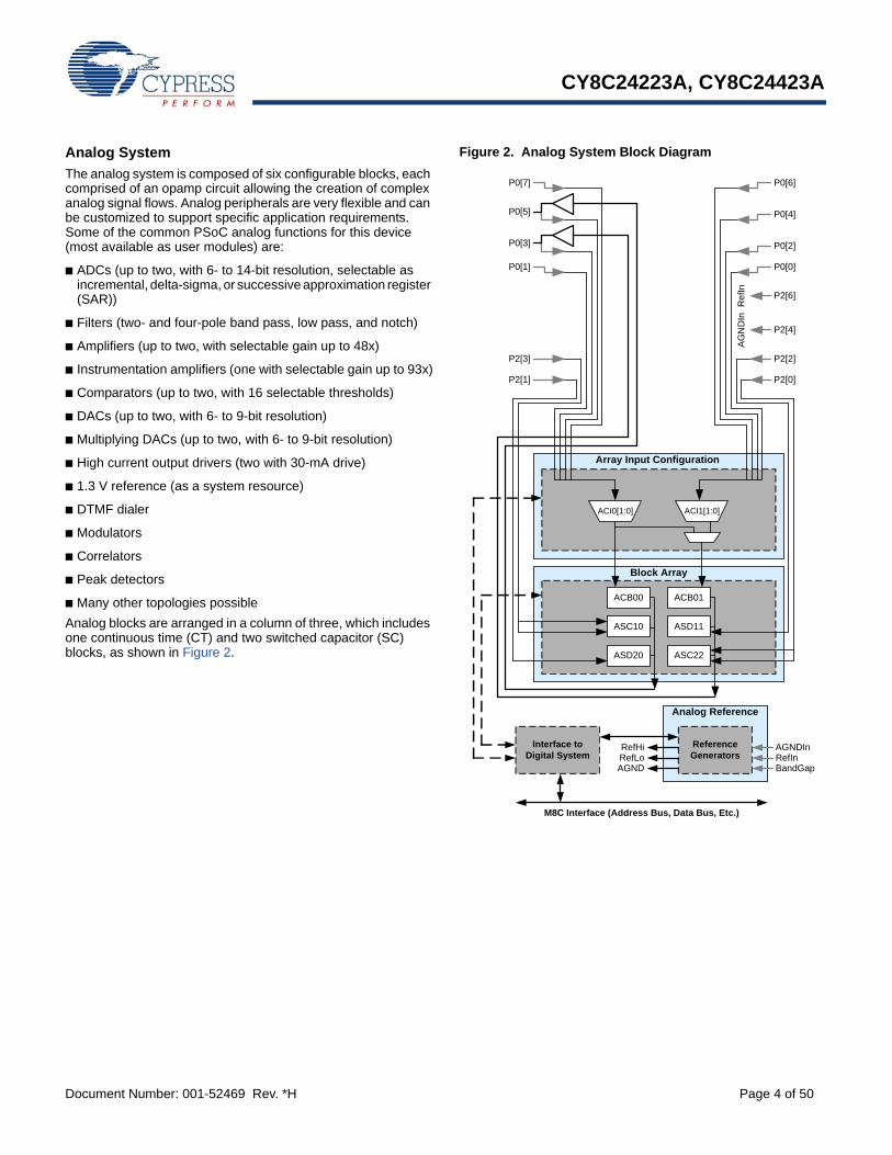
Analog System
The analog system is composed of six configurable blocks, each comprised of an opamp circuit allowing the creation of complex analog signal flows. Analog peripherals are very flexible and can be customized to support specific application requirements. Some of the common PSoC analog functions for this device (most available as user modules) are:
■ ADCs (up to two, with 6- to 14-bit resolution, selectable as incremental, delta-sigma, or successive approximation register (SAR))
■ Filters (two- and four-pole band pass, low pass, and notch)
■ Amplifiers (up to two, with selectable gain up to 48x)
■ Instrumentation amplifiers (one with selectable gain up to 93x)
■ Comparators (up to two, with 16 selectable thresholds)
■ DACs (up to two, with 6- to 9-bit resolution)
■ Multiplying DACs (up to two, with 6- to 9-bit resolution)
■ High current output drivers (two with 30-mA drive)
■ 1.3 V reference (as a system resource)
■ DTMF dialer
■ Modulators
■ Correlators
■ Peak detectors
■ Many other topologies possible
Analog blocks are arranged in a column of three, which includes one continuous time (CT) and two switched capacitor (SC) blocks, as shown in Figure 2.
Figure 2. Analog System Block Diagram
ACB01
Block Array
Array Input Configuration
ACI1[1:0]
ASD20
ACI0[1:0]
P0[4]
Ref
InA
GN
DIn
Reference Generators
AGNDIn
ASD11
Interface to Digital System
M8C Interface (Address Bus, Data Bus, Etc.)
Analog Reference
P0[6]
P0[2]
P0[0]
P2[6]
P2[4]
P2[2]
P2[0]
ASD11
ASC22
ACB00
ASC10
P0[7]
P0[5]
P0[3]
P0[1]
P2[3]
P2[1]
RefInBandGap
RefHiRefLoAGND
CY8C24223A, CY8C24423A
Document Number: 001-52469 Rev. *H Page 5 of 50
Additional System Resources
System resources, some of which have been previously listed, provide additional capability useful for complete systems. Additional resources include a multiplier, decimator, low voltage detection, and power-on reset (POR). Brief statements describing the merits of each system resource follow:
■ Digital clock dividers provide three customizable clock frequencies for use in applications. The clocks can be routed to both the digital and analog systems. Additional clocks can be generated using digital PSoC blocks as clock dividers.
■ A multiply accumulate (MAC) provides a fast 8-bit multiplier with 32-bit accumulate, to assist in both general math as well as digital filters.
■ The decimator provides a custom hardware filter for digital signal processing applications including the creation of delta-sigma ADCs.
■ The I2C module provides 0 to 400 kHz communication over two wires. Slave, master, and multimaster modes are all supported.
■ LVD interrupts can signal the application of falling voltage levels, while the advanced POR circuit eliminates the need for a system supervisor.
■ An internal 1.3-V voltage reference provides an absolute reference for the analog system, including ADCs and DACs.
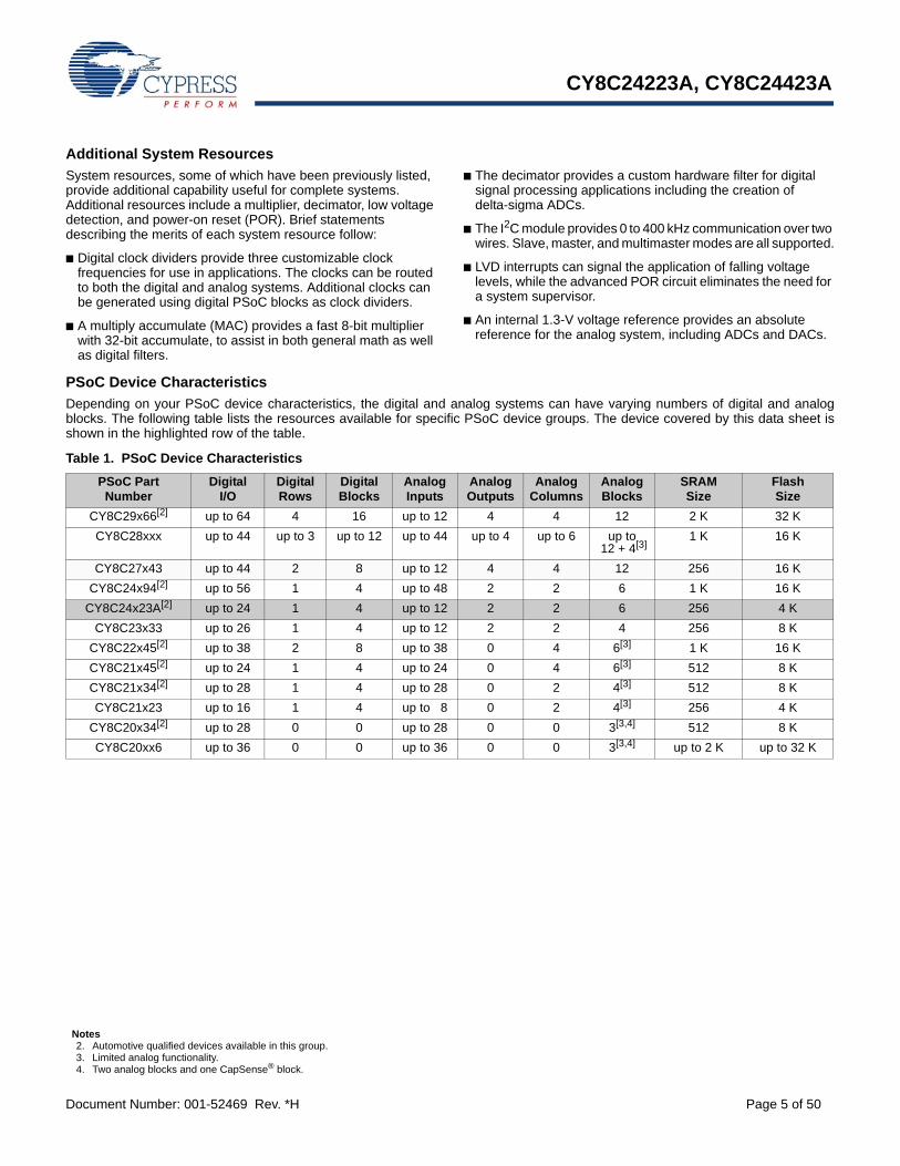
PSoC Device Characteristics
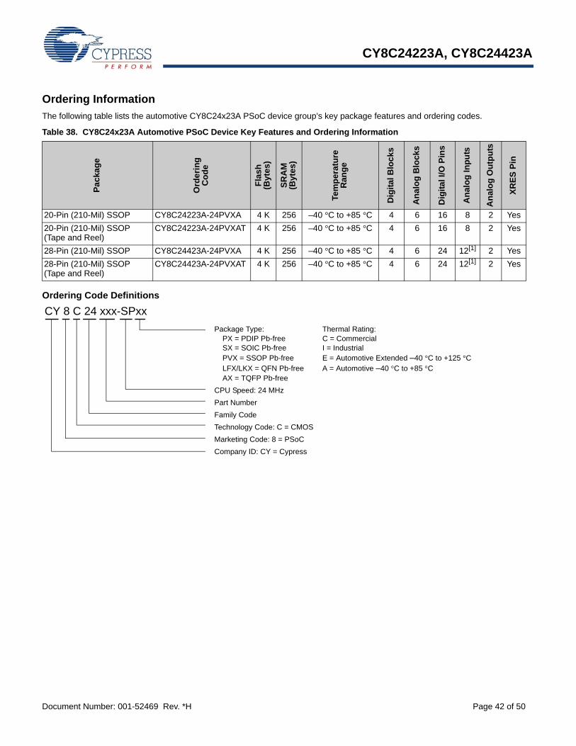
Depending on your PSoC device characteristics, the digital and analog systems can have varying numbers of digital and analogblocks. The following table lists the resources available for specific PSoC device groups. The device covered by this data sheet isshown in the highlighted row of the table.
Table 1. PSoC Device Characteristics
PSoC PartNumber
Digital I/O
Digital Rows
Digital Blocks
Analog Inputs
Analog Outputs
Analog Columns
Analog Blocks
SRAMSize
Flash Size
CY8C29x66[2] up to 64 4 16 up to 12 4 4 12 2 K 32 K
CY8C28xxx up to 44 up to 3 up to 12 up to 44 up to 4 up to 6 up to 12 + 4[3]
1 K 16 K
CY8C27x43 up to 44 2 8 up to 12 4 4 12 256 16 K
CY8C24x94[2] up to 56 1 4 up to 48 2 2 6 1 K 16 K
CY8C24x23A[2] up to 24 1 4 up to 12 2 2 6 256 4 K
CY8C23x33 up to 26 1 4 up to 12 2 2 4 256 8 K
CY8C22x45[2] up to 38 2 8 up to 38 0 4 6[3] 1 K 16 K
CY8C21x45[2] up to 24 1 4 up to 24 0 4 6[3] 512 8 K
CY8C21x34[2] up to 28 1 4 up to 28 0 2 4[3] 512 8 K
CY8C21x23 up to 16 1 4 up to 8 0 2 4[3] 256 4 K
CY8C20x34[2] up to 28 0 0 up to 28 0 0 3[3,4] 512 8 K
CY8C20xx6 up to 36 0 0 up to 36 0 0 3[3,4] up to 2 K up to 32 K
Notes2. Automotive qualified devices available in this group.3. Limited analog functionality.4. Two analog blocks and one CapSense® block.
CY8C24223A, CY8C24423A
Document Number: 001-52469 Rev. *H Page 6 of 50
Getting StartedFor in-depth information, along with detailed programming details, see the PSoC® Technical Reference Manual.
For up-to-date ordering, packaging, and electrical specification information, see the latest PSoC device datasheets on the web.
Application Notes
Cypress application notes are an excellent introduction to the wide variety of possible PSoC designs.
Development Kits
PSoC Development Kits are available online from and through a growing number of regional and global distributors, which include Arrow, Avnet, Digi-Key, Farnell, Future Electronics, and Newark.
Training
Free PSoC technical training (on demand, webinars, and workshops), which is available online via www.cypress.com, covers a wide variety of topics and skill levels to assist you in your designs.
CYPros Consultants
Certified PSoC consultants offer everything from technical assistance to completed PSoC designs. To contact or become a PSoC consultant go to the CYPros Consultants web site.
Solutions Library
Visit our growing library of solution focused designs. Here you can find various application designs that include firmware and hardware design files that enable you to complete your designs quickly.
Technical Support
Technical support – including a searchable Knowledge Base articles and technical forums – is also available online. If you cannot find an answer to your question, call our Technical Support hotline at 1-800-541-4736.
Development ToolsPSoC Designer™ is the revolutionary integrated design environment (IDE) that you can use to customize PSoC to meet your specific application requirements. PSoC Designer software accelerates system design and time to market. Develop your applications using a library of precharacterized analog and digital peripherals (called user modules) in a drag-and-drop design environment. Then, customize your design by leveraging the dynamically generated application programming interface (API) libraries of code. Finally, debug and test your designs with the integrated debug environment, including in-circuit emulation and standard software debug features. PSoC Designer includes:
■ Application editor graphical user interface (GUI) for device and user module configuration and dynamic reconfiguration
■ Extensive user module catalog
■ Integrated source-code editor (C and assembly)
■ Free C compiler with no size restrictions or time limits
■ Built-in debugger
■ In-circuit emulation
■ Built-in support for communication interfaces:❐ Hardware and software I2C slaves and masters❐ Full-speed USB 2.0❐ Up to four full-duplex universal asynchronous
receiver/transmitters (UARTs), SPI master and slave, and wireless
PSoC Designer supports the entire library of PSoC 1 devices and runs on Windows XP, Windows Vista, and Windows 7.
PSoC Designer Software Subsystems
Design Entry
In the chip-level view, choose a base device to work with. Then select different onboard analog and digital components that use the PSoC blocks, which are called user modules. Examples of user modules are ADCs, DACs, amplifiers, and filters. Configure the user modules for your chosen application and connect them to each other and to the proper pins. Then generate your project. This prepopulates your project with APIs and libraries that you can use to program your application.
The tool also supports easy development of multiple configurations and dynamic reconfiguration. Dynamic reconfiguration makes it possible to change configurations at run time. In essence, this allows you to use more than 100 percent of PSoC's resources for an application.
Code Generation Tools
The code generation tools work seamlessly within the PSoC Designer interface and have been tested with a full range of debugging tools. You can develop your design in C, assembly, or a combination of the two.
Assemblers. The assemblers allow you to merge assembly code seamlessly with C code. Link libraries automatically use absolute addressing or are compiled in relative mode, and are linked with other software modules to get absolute addressing.
C Language Compilers. C language compilers are available that support the PSoC family of devices. The products allow you to create complete C programs for the PSoC family devices. The optimizing C compilers provide all of the features of C, tailored to the PSoC architecture. They come complete with embedded libraries providing port and bus operations, standard keypad and display support, and extended math functionality.
Debugger
PSoC Designer has a debug environment that provides hardware in-circuit emulation, allowing you to test the program in a physical system while providing an internal view of the PSoC device. Debugger commands allow you to read and program and read and write data memory, and read and write I/O registers. You can read and write CPU registers, set and clear breakpoints, and provide program run, halt, and step control. The debugger also allows you to create a trace buffer of registers and memory locations of interest.
Online Help System
The online help system displays online, context-sensitive help. Designed for procedural and quick reference, each functional
subsystem has its own context-sensitive help. This system also provides tutorials and links to FAQs and an online support Forum to aid the designer.
In-Circuit Emulator
A low-cost, high-functionality in-circuit emulator (ICE) is available for development support. This hardware can program single devices.
The emulator consists of a base unit that connects to the PC using a USB port. The base unit is universal and operates with all PSoC devices. Emulation pods for each device family are available separately. The emulation pod takes the place of the PSoC device in the target board and performs full-speed (24 MHz) operation.
Designing with PSoC DesignerThe development process for the PSoC device differs from that of a traditional fixed function microprocessor. The configurable analog and digital hardware blocks give the PSoC architecture a unique flexibility that pays dividends in managing specification change during development and by lowering inventory costs. These configurable resources, called PSoC Blocks, have the ability to implement a wide variety of user-selectable functions.
The PSoC development process can be summarized in the following four steps:
1. Select User Modules
2. Configure User Modules
3. Organize and Connect
4. Generate, Verify, and Debug
Select Components
PSoC Designer provides a library of pre-built, pre-tested hardware peripheral components called "user modules." User modules make selecting and implementing peripheral devices, both analog and digital, simple.
Configure Components
Each of the User Modules you select establishes the basic register settings that implement the selected function. They also provide parameters and properties that allow you to tailor their
precise configuration to your particular application. For example, a PWM User Module configures one or more
digital PSoC blocks, one for each 8 bits of resolution. The user module parameters permit you to establish the pulse width and duty cycle. Configure the parameters and properties to corre-spond to your chosen application. Enter values directly or by selecting values from drop-down menus. All the user modules are documented in datasheets that may be viewed directly in PSoC Designer or on the Cypress website. These user module datasheets explain the internal operation of the User Module and provide performance specifications. Each datasheet describes the use of each user module parameter, and other information you may need to successfully implement your design.
Organize and Connect
You build signal chains at the chip level by interconnecting user modules to each other and the I/O pins. You perform the selection, configuration, and routing so that you have complete control over all on-chip resources.
Generate, Verify, and Debug
When you are ready to test the hardware configuration or move on to developing code for the project, you perform the "Generate Configuration Files" step. This causes PSoC Designer to generate source code that automatically configures the device to your specification and provides the software for the system. The generated code provides application programming interfaces (APIs) with high-level functions to control and respond to hardware events at run time and interrupt service routines that you can adapt as needed.
A complete code development environment allows you to develop and customize your applications in C, assembly language, or both.
The last step in the development process takes place inside PSoC Designer's Debugger (access by clicking the Connect icon). PSoC Designer downloads the HEX image to the ICE where it runs at full speed. PSoC Designer debugging capabil-ities rival those of systems costing many times more. In addition
to traditional single-step, run-to-breakpoint and watch-variable features, the debug interface provides a large trace buffer and allows you to define complex breakpoint events that include monitoring address and data bus values, memory locations and external signals.
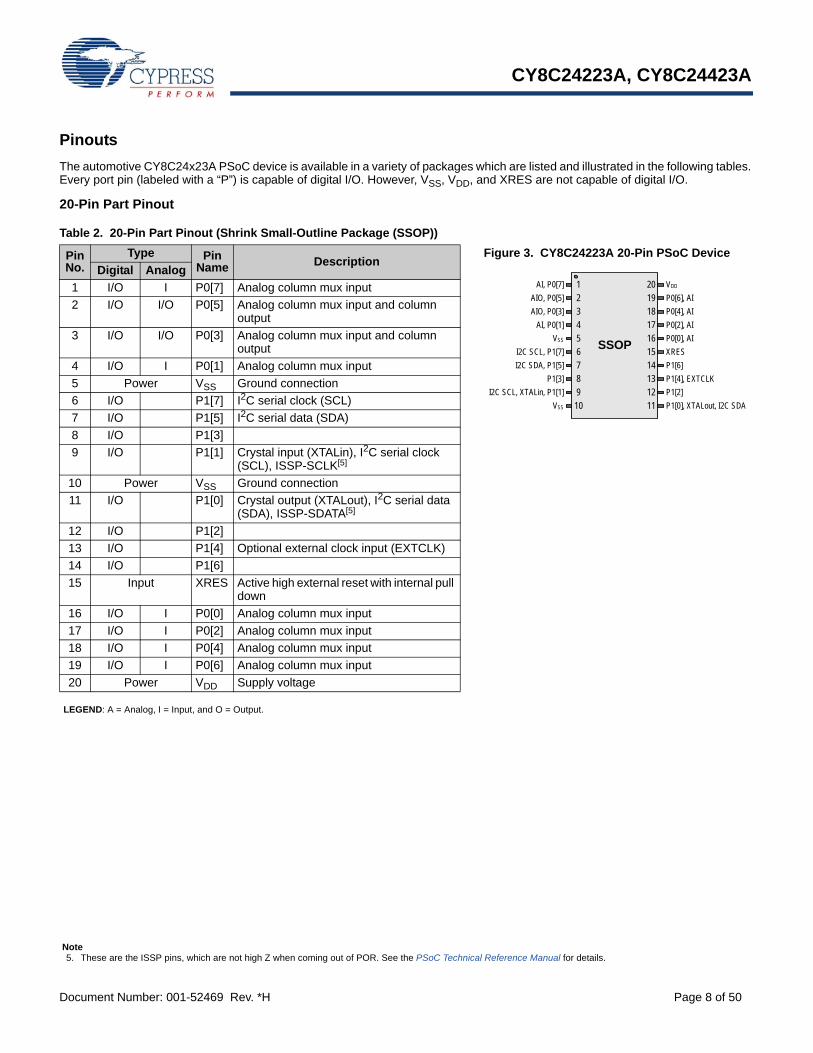
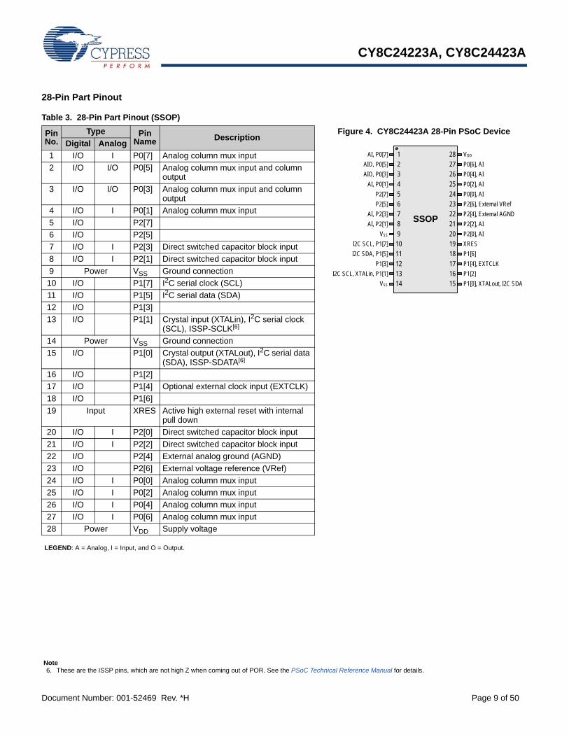
The automotive CY8C24x23A PSoC device is available in a variety of packages which are listed and illustrated in the following tables. Every port pin (labeled with a “P”) is capable of digital I/O. However, VSS, VDD, and XRES are not capable of digital I/O.
20-Pin Part Pinout
Note5. These are the ISSP pins, which are not high Z when coming out of POR. See the PSoC Technical Reference Manual for details.
Table 2. 20-Pin Part Pinout (Shrink Small-Outline Package (SSOP))
Pin No.
Type Pin Name Description
Figure 3. CY8C24223A 20-Pin PSoC Device
Digital Analog
1 I/O I P0[7] Analog column mux input
2 I/O I/O P0[5] Analog column mux input and column output
3 I/O I/O P0[3] Analog column mux input and column output
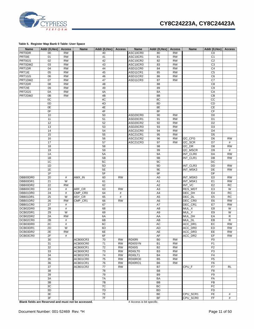
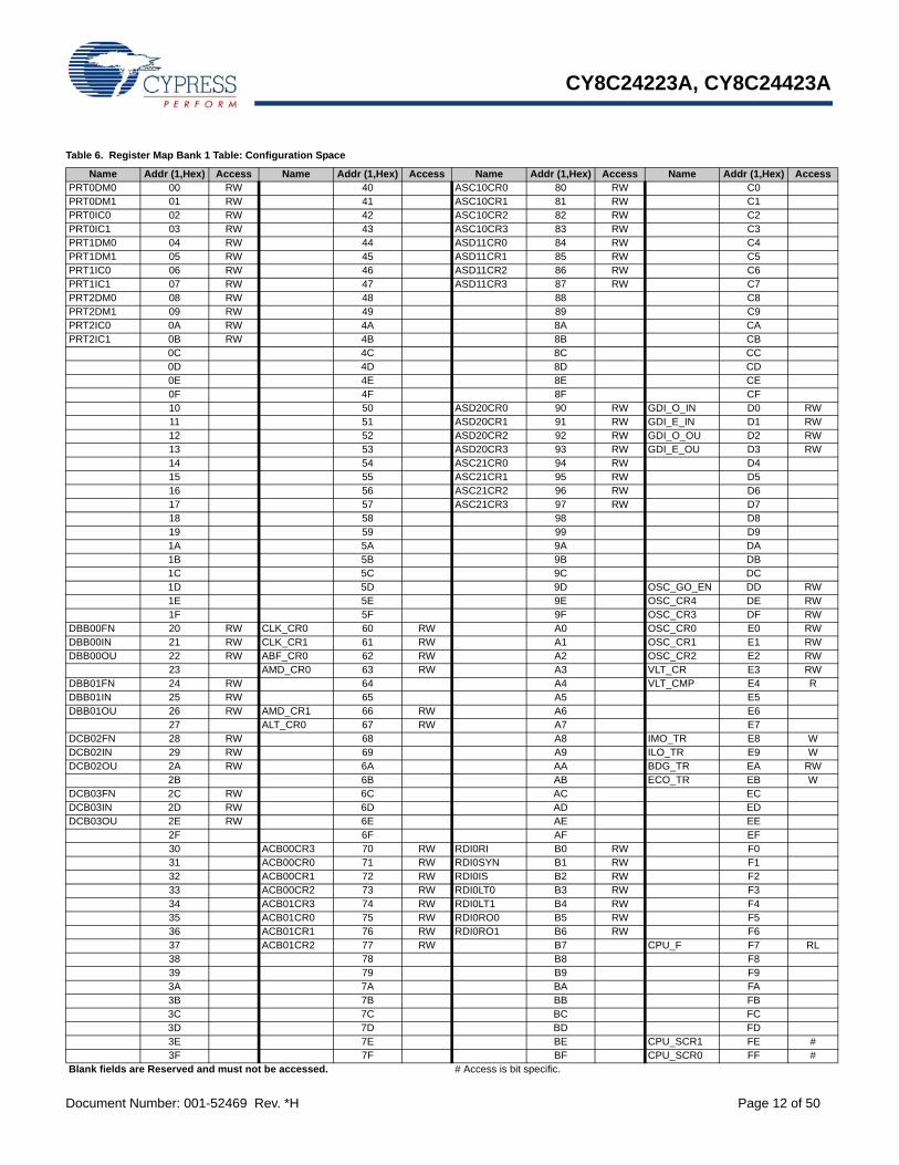
This section lists the registers of the automotive CY8C24x23A PSoC device. For detailed register information, refer to the PSoC Technical Reference Manual.
The register conventions specific to this section are listed in the following table.
Register Mapping Tables
The PSoC device has a total register address space of 512 bytes. The register space is referred to as I/O space and is divided into two banks, bank 0 and bank 1. The XIO bit in the Flag register (CPU_F) determines which bank the user is currently in. When the XIO bit is set to ‘1’, the user is in bank 1.
Note In the following register mapping tables, blank fields are Reserved and must not be accessed.Table 4. Abbreviations
Blank fields are Reserved and must not be accessed. # Access is bit specific.
CY8C24223A, CY8C24423A
Document Number: 001-52469 Rev. *H Page 13 of 50
Electrical Specifications
This section presents the DC and AC electrical specifications of the automotive CY8C24x23A PSoC devices. For the latest electrical specifications, visit http://www.cypress.com.
Specifications are valid for –40 °C TA 85 °C and TJ 100 °C, except where noted.
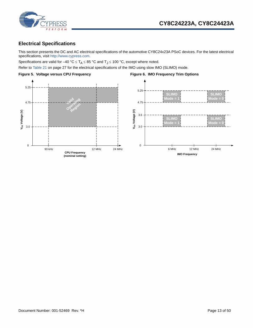
Refer to Table 21 on page 27 for the electrical specifications of the IMO using slow IMO (SLIMO) mode.
Figure 5. Voltage versus CPU Frequency Figure 6. IMO Frequency Trim Options
Exceeding maximum ratings may shorten the useful life of the device. User guidelines are not tested.
Operating Temperature
Table 7. Absolute Maximum Ratings
Symbol Description Min Typ Max Units Notes
TSTG Storage temperature –55 25 +100 °C Higher storage temperatures reduce data retention time. Recommended storage temperature is +25 °C ± 25 °C. Time spent in storage at a temperature greater than 65 °C counts toward the FlashDR electrical specification in Table 20 on page 26.
TBAKETEMP Bake temperature – 125 See package
label
C
tBAKETIME Bake time See package
label
– 72 Hours
TA Ambient temperature with power applied –40 – +85 °C
VDD Supply voltage on VDD relative to VSS –0.5 – +6.0 V
VIO DC input voltage VSS – 0.5 – VDD + 0.5 V
VIOZ DC voltage applied to tristate VSS – 0.5 – VDD + 0.5 V
IMIO Maximum current into any port pin –25 – +50 mA
ESD Electrostatic discharge voltage 2000 – – V Human body model ESD.
LU Latch up current – – 200 mA
Table 8. Operating Temperature
Symbol Description Min Typ Max Units Notes
TA Ambient temperature –40 – +85 °C
TJ Junction temperature –40 – +100 °C The temperature rise from ambient to junction is package specific. See Table 33 on page 37. The user must limit the power consumption to comply with this requirement.
CY8C24223A, CY8C24423A
Document Number: 001-52469 Rev. *H Page 15 of 50
DC Electrical Characteristics
DC Chip-Level Specifications
Table 9 lists the guaranteed maximum and minimum specifications for the voltage and temperature ranges: 4.75 V to 5.25 V and –40 °C TA 85 °C, 3.0 V to 3.6 V and –40 °C TA 85 °C, respectively. Typical parameters apply to 5 V and 3.3 V at 25 °C and are for design guidance only.
Table 9. DC Chip-Level Specifications
Symbol Description Min Typ Max Units Notes
VDD Supply voltage 3.0 – 5.25 V See DC POR and LVD specifications, Table 19 on page 25.
IDD Supply current – 5 8 mA Conditions are VDD = 5.0 V, CPU = 3 MHz, 48 MHz disabled, VC1 = 1.5 MHz, VC2 = 93.75 kHz, VC3 = 93.75 kHz, analog power = off. IMO = 24 MHz.
IDD3 Supply current – 3.3 6.0 mA Conditions are VDD = 3.3 V, CPU = 3 MHz, 48 MHz disabled, VC1 = 1.5 MHz, VC2 = 93.75 kHz, VC3 = 93.75 kHz, Analog power = off. IMO = 24 MHz.
ISB Sleep (mode) current with POR, LVD, sleep timer, and WDT.[7]
– 3 6.5 A VDD = 3.3 V, –40 °C TA 55 °C, Analog power = off.
ISBH Sleep (mode) current with POR, LVD, sleep timer, and WDT at high temperature.[7]
– 4 25 A VDD = 3.3 V, 55 °C < TA 85 °C, Analog power = off.
ISBXTL Sleep (mode) current with POR, LVD, sleep timer, WDT, and external crystal.[7]
– 4 7.5 A Conditions are with properly loaded, 1 W max, 32.768 kHz crystal. VDD = 3.3 V, –40 °C TA 55 °C, Analog power = off.
ISBXTLH Sleep (mode) current with POR, LVD, sleep timer, WDT, and external crystal at high temperature.[7]
– 5 26 A Conditions are with properly loaded, 1 W max, 32.768 kHz crystal. VDD = 3.3 V, 55 °C < TA 85 °C, Analog power = off.
VREF Reference voltage (bandgap) 1.28 1.30 1.32 V Trimmed for appropriate VDD.
Note7. Standby current includes all functions (POR, LVD, WDT, sleep timer) needed for reliable system operation. This must be compared with devices that have similar
functions enabled.
CY8C24223A, CY8C24423A
Document Number: 001-52469 Rev. *H Page 16 of 50
DC GPIO Specifications
Table 10 lists the guaranteed maximum and minimum specifications for the voltage and temperature ranges: 4.75 V to 5.25 V and –40 °C TA 85 °C, 3.0 V to 3.6 V and –40 °C TA 85 °C, respectively. Typical parameters apply to 5 V and 3.3 V at 25 °C and are for design guidance only.
Table 10. DC GPIO Specifications
Symbol Description Min Typ Max Units Notes
RPU Pull-up resistor 4 5.6 8 k
RPD Pull-down resistor 4 5.6 8 k Also applies to the internal pull-downresistor on the XRES pin.
VOH High output level VDD – 1.0 – – V IOH = 10 mA, VDD = 4.75 to 5.25 V (maximum 40 mA on even port pins (for example, P0[2], P1[4]), maximum 40 mA on odd port pins (for example, P0[3], P1[5])). 80 mA maximum combined IOH budget.
VOL Low output level – – 0.75 V IOL = 25 mA, VDD = 4.75 to 5.25 V (maximum 100 mA on even port pins (for example, P0[2], P1[4]), maximum 100 mA on odd port pins (for example, P0[3], P1[5])). 150 mA maximum combined IOL budget.
IOH High-level source current 10 – – mA VOH VDD – 1.0 V, see the limitations of the total current in the note for VOH.
IOL Low-level sink current 25 – – mA VOL 0.75 V, see the limitations of the total current in the note for VOL.
VIL Input low level – – 0.8 V
VIH Input high level 2.1 – V
VH Input hysteresis – 60 – mV
IIL Input leakage (absolute value) – 1 – nA Gross tested to 1 A.
CIN Capacitive load on pins as input – 3.5 10 pF Package and pin dependent. TA = 25 °C
COUT Capacitive load on pins as output – 3.5 10 pF Package and pin dependent.TA = 25 °C
CY8C24223A, CY8C24423A
Document Number: 001-52469 Rev. *H Page 17 of 50
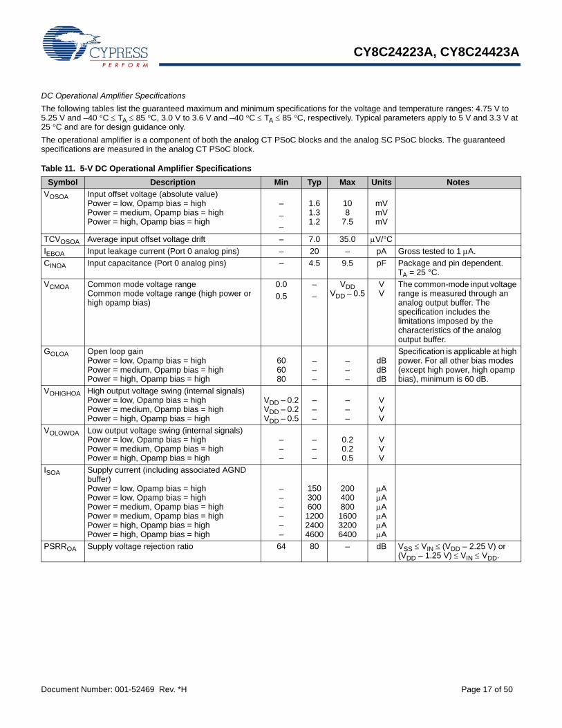
DC Operational Amplifier Specifications
The following tables list the guaranteed maximum and minimum specifications for the voltage and temperature ranges: 4.75 V to 5.25 V and –40 °C TA 85 °C, 3.0 V to 3.6 V and –40 °C TA 85 °C, respectively. Typical parameters apply to 5 V and 3.3 V at 25 °C and are for design guidance only.
The operational amplifier is a component of both the analog CT PSoC blocks and the analog SC PSoC blocks. The guaranteed specifications are measured in the analog CT PSoC block.
Table 11. 5-V DC Operational Amplifier Specifications
Symbol Description Min Typ Max Units Notes
VOSOA Input offset voltage (absolute value) Power = low, Opamp bias = highPower = medium, Opamp bias = highPower = high, Opamp bias = high
– 1.6 1.3 1.2
10 8
7.5
mV mV mV
–
–
TCVOSOA Average input offset voltage drift – 7.0 35.0 V/°C
IEBOA Input leakage current (Port 0 analog pins) – 20 – pA Gross tested to 1 A.
CINOA Input capacitance (Port 0 analog pins) – 4.5 9.5 pF Package and pin dependent. TA = 25 °C.
VCMOA Common mode voltage rangeCommon mode voltage range (high power or high opamp bias)
0.0 – VDDVDD – 0.5
VV
The common-mode input voltage range is measured through an analog output buffer. The specification includes the limitations imposed by the characteristics of the analog output buffer.
PSRROA Supply voltage rejection ratio 64 80 – dB VSS VIN (VDD – 2.25 V) or (VDD – 1.25 V) VIN VDD.
CY8C24223A, CY8C24423A
Document Number: 001-52469 Rev. *H Page 18 of 50
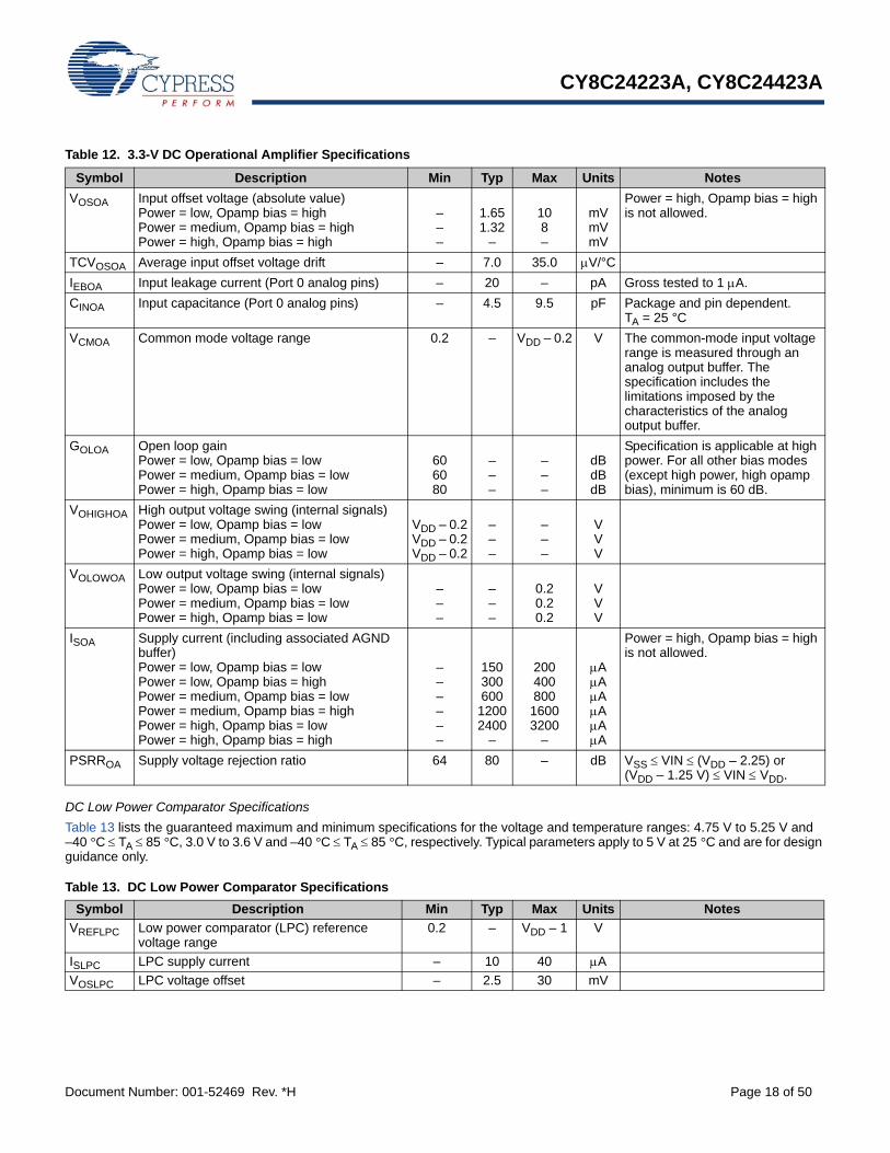
DC Low Power Comparator Specifications
Table 13 lists the guaranteed maximum and minimum specifications for the voltage and temperature ranges: 4.75 V to 5.25 V and –40 °C TA 85 °C, 3.0 V to 3.6 V and –40 °C TA 85 °C, respectively. Typical parameters apply to 5 V at 25 °C and are for design guidance only.
Table 12. 3.3-V DC Operational Amplifier Specifications
Symbol Description Min Typ Max Units Notes
VOSOA Input offset voltage (absolute value) Power = low, Opamp bias = highPower = medium, Opamp bias = highPower = high, Opamp bias = high
–––
1.65 1.32
–
10 8 –
mV mV mV
Power = high, Opamp bias = high is not allowed.
TCVOSOA Average input offset voltage drift – 7.0 35.0 V/°C
IEBOA Input leakage current (Port 0 analog pins) – 20 – pA Gross tested to 1 A.
CINOA Input capacitance (Port 0 analog pins) – 4.5 9.5 pF Package and pin dependent. TA = 25 °C
VCMOA Common mode voltage range 0.2 – VDD – 0.2 V The common-mode input voltage range is measured through an analog output buffer. The specification includes the limitations imposed by the characteristics of the analog output buffer.
PSRROA Supply voltage rejection ratio 64 80 – dB VSS VIN (VDD – 2.25) or (VDD – 1.25 V) VIN VDD.
Table 13. DC Low Power Comparator Specifications
Symbol Description Min Typ Max Units Notes
VREFLPC Low power comparator (LPC) reference voltage range
0.2 – VDD – 1 V
ISLPC LPC supply current – 10 40 A
VOSLPC LPC voltage offset – 2.5 30 mV
CY8C24223A, CY8C24423A
Document Number: 001-52469 Rev. *H Page 19 of 50
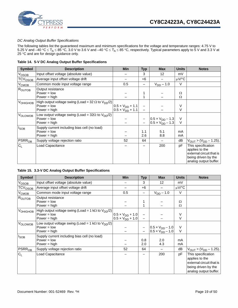
DC Analog Output Buffer Specifications
The following tables list the guaranteed maximum and minimum specifications for the voltage and temperature ranges: 4.75 V to 5.25 V and –40 °C TA 85 °C, 3.0 V to 3.6 V and –40 °C TA 85 °C, respectively. Typical parameters apply to 5 V and 3.3 V at 25 °C and are for design guidance only.
Table 14. 5-V DC Analog Output Buffer Specifications
Symbol Description Min Typ Max Units Notes
VOSOB Input offset voltage (absolute value) – 3 12 mV
TCVOSOB Average input offset voltage drift – +6 – V/°C
VCMOB Common mode input voltage range 0.5 – VDD – 1.0 V
ROUTOB Output resistancePower = lowPower = high
––
11
––
VOHIGHOB High output voltage swing (Load = 32 to VDD/2)Power = lowPower = high
0.5 × VDD + 1.10.5 × VDD + 1.1
––
––
VV
VOLOWOB Low output voltage swing (Load = 32 to VDD/2)Power = lowPower = high
––
––
0.5 × VDD – 1.30.5 × VDD – 1.3
VV
ISOB Supply current including bias cell (no load)Power = lowPower = high
––
1.12.6
5.18.8
mAmA
PSRROB Supply voltage rejection ratio 52 64 – dB VOUT > (VDD – 1.25).
CL Load Capacitance – – 200 pF This specification applies to the external circuit that is being driven by the analog output buffer.
Table 15. 3.3-V DC Analog Output Buffer Specifications
Symbol Description Min Typ Max Units Notes
VOSOB Input offset voltage (absolute value) – 3 12 mV
TCVOSOB Average input offset voltage drift – +6 – V/°C
VCMOB Common mode input voltage range 0.5 – VDD – 1.0 V
ROUTOB Output resistancePower = lowPower = high
––
11
––
VOHIGHOB High output voltage swing (Load = 1 k to VDD/2)Power = lowPower = high
0.5 × VDD + 1.00.5 × VDD + 1.0
––
––
VV
VOLOWOB Low output voltage swing (Load = 1 k to VDD/2)Power = lowPower = high
––
––
0.5 × VDD – 1.00.5 × VDD – 1.0
VV
ISOB Supply current including bias cell (no load)Power = lowPower = high
––
0.82.0
2.04.3
mAmA
PSRROB Supply voltage rejection ratio 52 64 – dB VOUT > (VDD – 1.25).
CL Load Capacitance – – 200 pF This specification applies to the external circuit that is being driven by the analog output buffer.
CY8C24223A, CY8C24423A
Document Number: 001-52469 Rev. *H Page 20 of 50
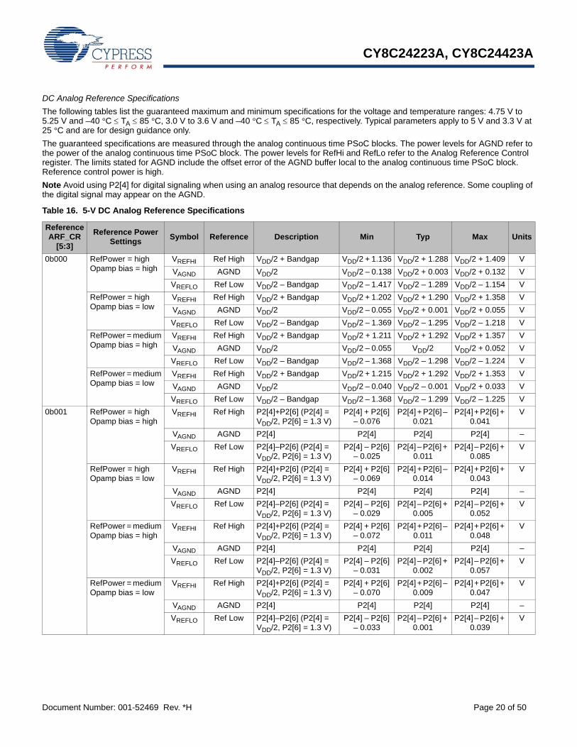
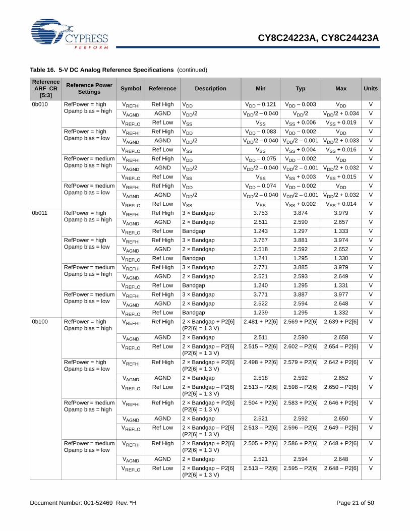
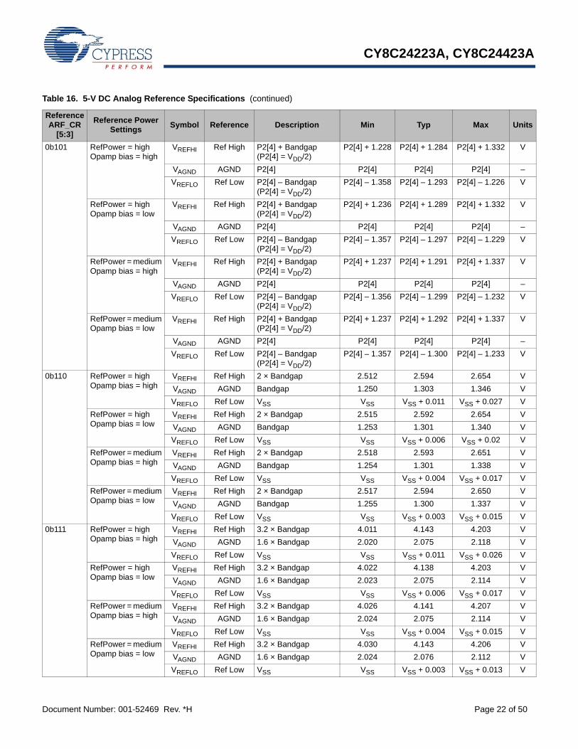
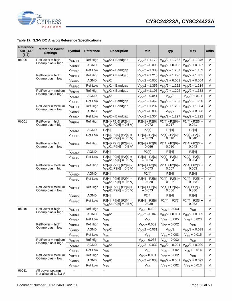
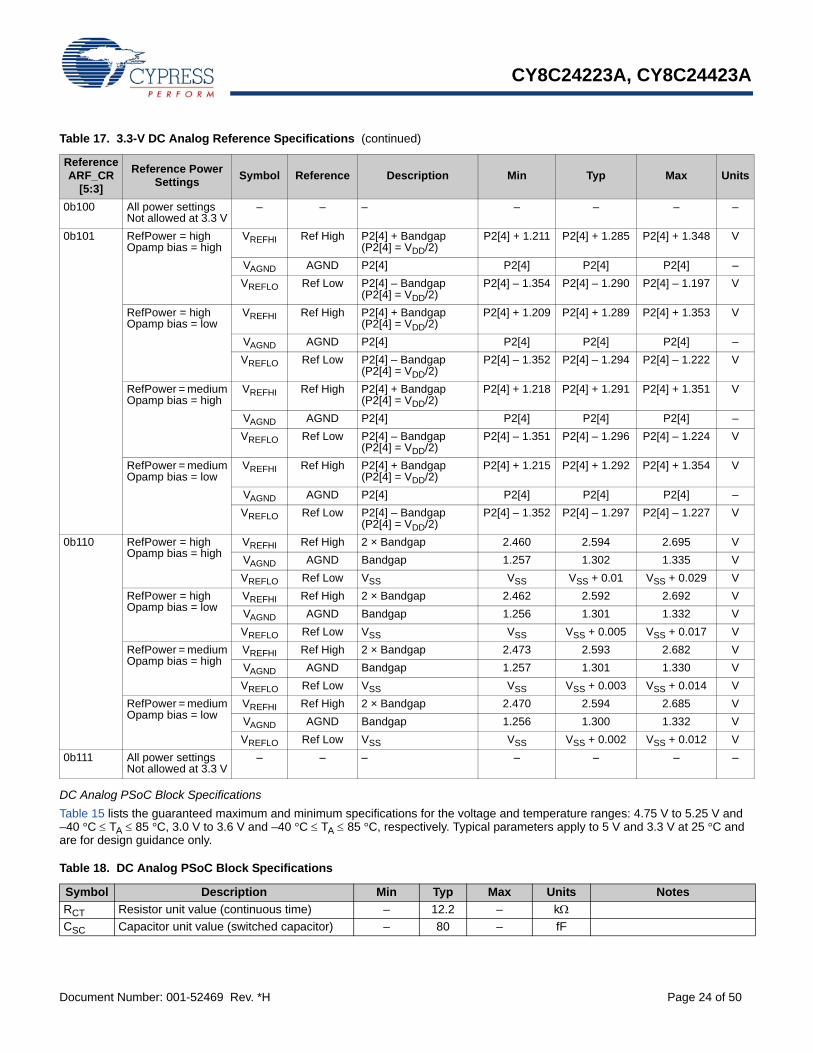
DC Analog Reference Specifications
The following tables list the guaranteed maximum and minimum specifications for the voltage and temperature ranges: 4.75 V to 5.25 V and –40 °C TA 85 °C, 3.0 V to 3.6 V and –40 °C TA 85 °C, respectively. Typical parameters apply to 5 V and 3.3 V at 25 °C and are for design guidance only.
The guaranteed specifications are measured through the analog continuous time PSoC blocks. The power levels for AGND refer to the power of the analog continuous time PSoC block. The power levels for RefHi and RefLo refer to the Analog Reference Control register. The limits stated for AGND include the offset error of the AGND buffer local to the analog continuous time PSoC block. Reference control power is high.
Note Avoid using P2[4] for digital signaling when using an analog resource that depends on the analog reference. Some coupling of the digital signal may appear on the AGND.
Table 16. 5-V DC Analog Reference Specifications
Reference ARF_CR
[5:3]
Reference Power Settings
Symbol Reference Description Min Typ Max Units
0b000 RefPower = highOpamp bias = high
VREFHI Ref High VDD/2 + Bandgap VDD/2 + 1.136 VDD/2 + 1.288 VDD/2 + 1.409 V
Table 15 lists the guaranteed maximum and minimum specifications for the voltage and temperature ranges: 4.75 V to 5.25 V and –40 °C TA 85 °C, 3.0 V to 3.6 V and –40 °C TA 85 °C, respectively. Typical parameters apply to 5 V and 3.3 V at 25 °C and are for design guidance only.
0b100 All power settingsNot allowed at 3.3 V
– – – – – – –
0b101 RefPower = highOpamp bias = high
VREFHI Ref High P2[4] + Bandgap (P2[4] = VDD/2)
P2[4] + 1.211 P2[4] + 1.285 P2[4] + 1.348 V
VAGND AGND P2[4] P2[4] P2[4] P2[4] –
VREFLO Ref Low P2[4] – Bandgap (P2[4] = VDD/2)
P2[4] – 1.354 P2[4] – 1.290 P2[4] – 1.197 V
RefPower = highOpamp bias = low
VREFHI Ref High P2[4] + Bandgap (P2[4] = VDD/2)
P2[4] + 1.209 P2[4] + 1.289 P2[4] + 1.353 V
VAGND AGND P2[4] P2[4] P2[4] P2[4] –
VREFLO Ref Low P2[4] – Bandgap (P2[4] = VDD/2)
P2[4] – 1.352 P2[4] – 1.294 P2[4] – 1.222 V
RefPower = mediumOpamp bias = high
VREFHI Ref High P2[4] + Bandgap (P2[4] = VDD/2)
P2[4] + 1.218 P2[4] + 1.291 P2[4] + 1.351 V
VAGND AGND P2[4] P2[4] P2[4] P2[4] –
VREFLO Ref Low P2[4] – Bandgap (P2[4] = VDD/2)
P2[4] – 1.351 P2[4] – 1.296 P2[4] – 1.224 V
RefPower = mediumOpamp bias = low
VREFHI Ref High P2[4] + Bandgap (P2[4] = VDD/2)
P2[4] + 1.215 P2[4] + 1.292 P2[4] + 1.354 V
VAGND AGND P2[4] P2[4] P2[4] P2[4] –
VREFLO Ref Low P2[4] – Bandgap (P2[4] = VDD/2)
P2[4] – 1.352 P2[4] – 1.297 P2[4] – 1.227 V
0b110 RefPower = highOpamp bias = high
VREFHI Ref High 2 × Bandgap 2.460 2.594 2.695 V
VAGND AGND Bandgap 1.257 1.302 1.335 V
VREFLO Ref Low VSS VSS VSS + 0.01 VSS + 0.029 V
RefPower = highOpamp bias = low
VREFHI Ref High 2 × Bandgap 2.462 2.592 2.692 V
VAGND AGND Bandgap 1.256 1.301 1.332 V
VREFLO Ref Low VSS VSS VSS + 0.005 VSS + 0.017 V
RefPower = mediumOpamp bias = high
VREFHI Ref High 2 × Bandgap 2.473 2.593 2.682 V
VAGND AGND Bandgap 1.257 1.301 1.330 V
VREFLO Ref Low VSS VSS VSS + 0.003 VSS + 0.014 V
RefPower = mediumOpamp bias = low
VREFHI Ref High 2 × Bandgap 2.470 2.594 2.685 V
VAGND AGND Bandgap 1.256 1.300 1.332 V
VREFLO Ref Low VSS VSS VSS + 0.002 VSS + 0.012 V
0b111 All power settingsNot allowed at 3.3 V
– – – – – – –
Table 17. 3.3-V DC Analog Reference Specifications (continued)
Reference ARF_CR
[5:3]
Reference Power Settings
Symbol Reference Description Min Typ Max Units
Table 18. DC Analog PSoC Block Specifications
Symbol Description Min Typ Max Units Notes
RCT Resistor unit value (continuous time) – 12.2 – kCSC Capacitor unit value (switched capacitor) – 80 – fF
CY8C24223A, CY8C24423A
Document Number: 001-52469 Rev. *H Page 25 of 50
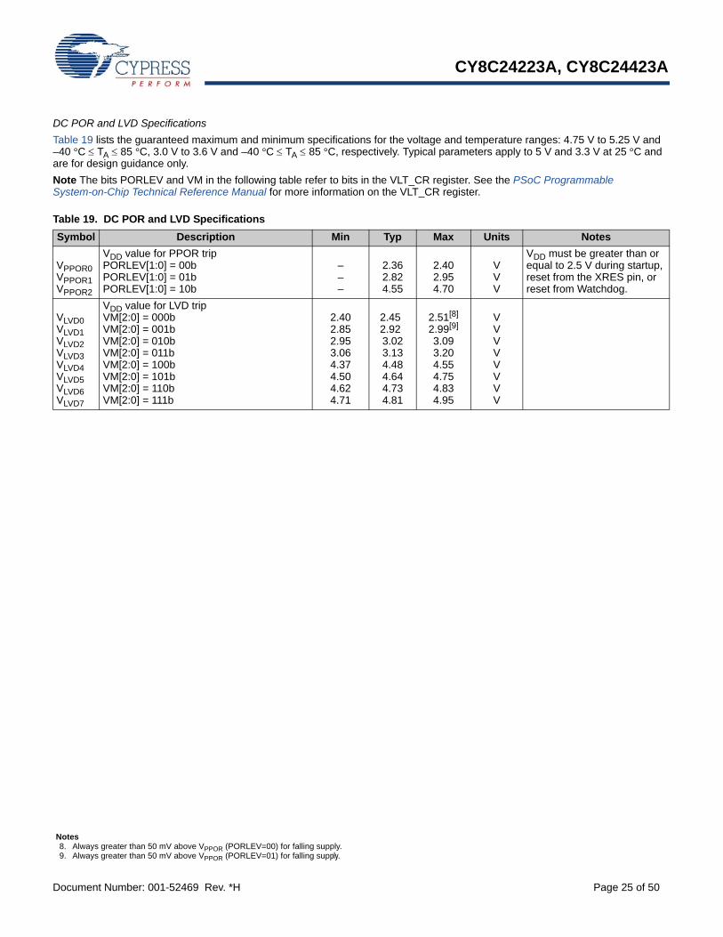
DC POR and LVD Specifications
Table 19 lists the guaranteed maximum and minimum specifications for the voltage and temperature ranges: 4.75 V to 5.25 V and –40 °C TA 85 °C, 3.0 V to 3.6 V and –40 °C TA 85 °C, respectively. Typical parameters apply to 5 V and 3.3 V at 25 °C and are for design guidance only.
Note The bits PORLEV and VM in the following table refer to bits in the VLT_CR register. See the PSoC Programmable System-on-Chip Technical Reference Manual for more information on the VLT_CR register.
Table 19. DC POR and LVD Specifications
Symbol Description Min Typ Max Units Notes
VPPOR0VPPOR1VPPOR2
VDD value for PPOR tripPORLEV[1:0] = 00bPORLEV[1:0] = 01bPORLEV[1:0] = 10b
–––
2.362.824.55
2.402.954.70
VVV
VDD must be greater than or equal to 2.5 V during startup, reset from the XRES pin, or reset from Watchdog.
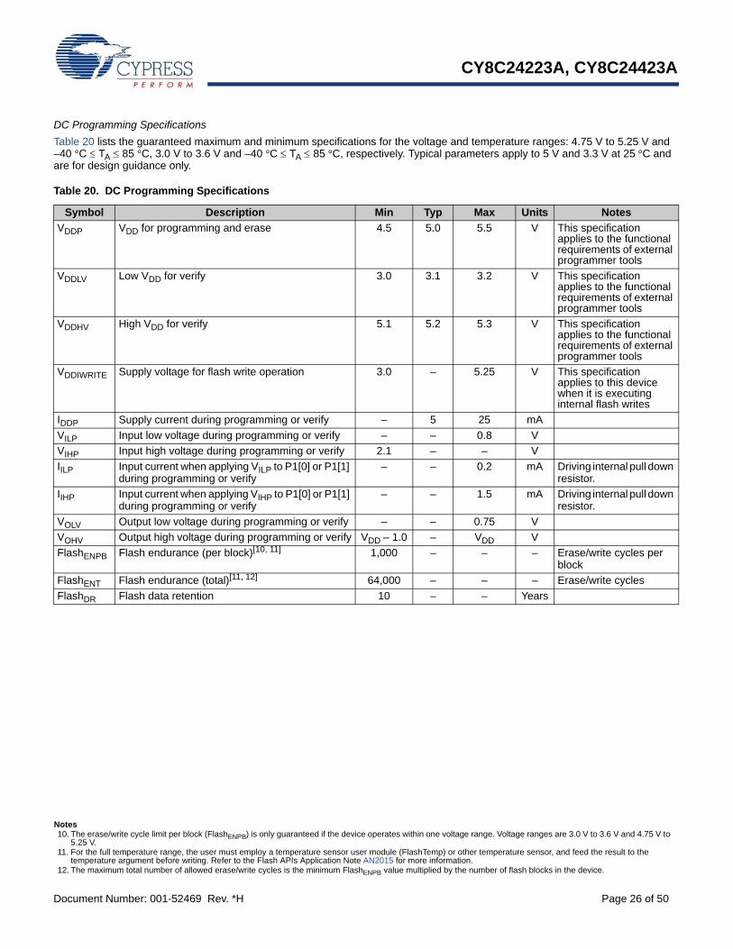
Table 20 lists the guaranteed maximum and minimum specifications for the voltage and temperature ranges: 4.75 V to 5.25 V and –40 °C TA 85 °C, 3.0 V to 3.6 V and –40 °C TA 85 °C, respectively. Typical parameters apply to 5 V and 3.3 V at 25 °C and are for design guidance only.
Table 20. DC Programming Specifications
Symbol Description Min Typ Max Units Notes
VDDP VDD for programming and erase 4.5 5.0 5.5 V This specification applies to the functional requirements of external programmer tools
VDDLV Low VDD for verify 3.0 3.1 3.2 V This specification applies to the functional requirements of external programmer tools
VDDHV High VDD for verify 5.1 5.2 5.3 V This specification applies to the functional requirements of external programmer tools
VDDIWRITE Supply voltage for flash write operation 3.0 – 5.25 V This specification applies to this device when it is executing internal flash writes
IDDP Supply current during programming or verify – 5 25 mA
VILP Input low voltage during programming or verify – – 0.8 V
VIHP Input high voltage during programming or verify 2.1 – – V
IILP Input current when applying VILP to P1[0] or P1[1] during programming or verify
– – 0.2 mA Driving internal pull down resistor.
IIHP Input current when applying VIHP to P1[0] or P1[1] during programming or verify
– – 1.5 mA Driving internal pull down resistor.
VOLV Output low voltage during programming or verify – – 0.75 V
VOHV Output high voltage during programming or verify VDD – 1.0 – VDD V
Notes10. The erase/write cycle limit per block (FlashENPB) is only guaranteed if the device operates within one voltage range. Voltage ranges are 3.0 V to 3.6 V and 4.75 V to
5.25 V.11. For the full temperature range, the user must employ a temperature sensor user module (FlashTemp) or other temperature sensor, and feed the result to the
temperature argument before writing. Refer to the Flash APIs Application Note AN2015 for more information.12. The maximum total number of allowed erase/write cycles is the minimum FlashENPB value multiplied by the number of flash blocks in the device.
Table 21 lists the guaranteed maximum and minimum specifications for the voltage and temperature ranges: 4.75 V to 5.25 V and –40 °C TA 85 °C, 3.0 V to 3.6 V and –40 °C TA 85 °C, respectively. Typical parameters apply to 5 V and 3.3 V at 25 °C and are for design guidance only.
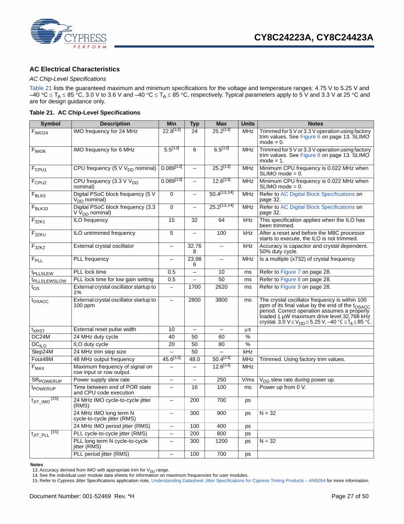
Table 21. AC Chip-Level Specifications
Symbol Description Min Typ Max Units NotesFIMO24 IMO frequency for 24 MHz 22.8[13] 24 25.2[13] MHz Trimmed for 5 V or 3.3 V operation using factory
trim values. See Figure 6 on page 13. SLIMO mode = 0.
FIMO6 IMO frequency for 6 MHz 5.5[13] 6 6.5[13] MHz Trimmed for 5 V or 3.3 V operation using factory trim values. See Figure 6 on page 13. SLIMO mode = 1.
FCPU1 CPU frequency (5 V VDD nominal) 0.089[13] – 25.2[13] MHz Minimum CPU frequency is 0.022 MHz when SLIMO mode = 0.
FCPU2 CPU frequency (3.3 V VDD nominal)
0.089[13] – 12.6[13] MHz Minimum CPU frequency is 0.022 MHz when SLIMO mode = 0.
FBLK5 Digital PSoC block frequency (5 V VDD nominal)
0 – 50.4[13,14] MHz Refer to AC Digital Block Specifications on page 32.
FBLK33 Digital PSoC block frequency (3.3 V VDD nominal)
0 – 25.2[13,14] MHz Refer to AC Digital Block Specifications on page 32.
F32K1 ILO frequency 15 32 64 kHz This specification applies when the ILO has been trimmed.
F32KU ILO untrimmed frequency 5 – 100 kHz After a reset and before the M8C processor starts to execute, the ILO is not trimmed.
F32K2 External crystal oscillator – 32.768
– kHz Accuracy is capacitor and crystal dependent. 50% duty cycle.
FPLL PLL frequency – 23.986
– MHz Is a multiple (x732) of crystal frequency.
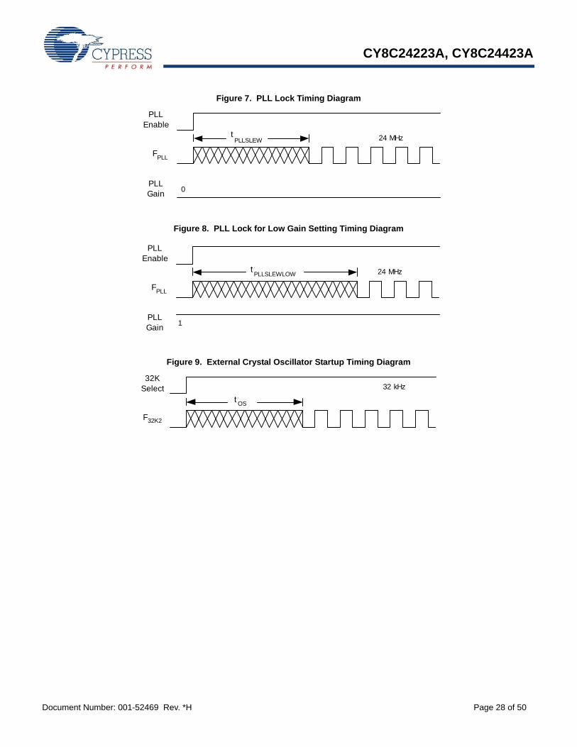
tPLLSLEW PLL lock time 0.5 – 10 ms Refer to Figure 7 on page 28.tPLLSLEWSLOW PLL lock time for low gain setting 0.5 – 50 ms Refer to Figure 8 on page 28.tOS External crystal oscillator startup to
1%– 1700 2620 ms Refer to Figure 9 on page 28.
tOSACC External crystal oscillator startup to 100 ppm
– 2800 3800 ms The crystal oscillator frequency is within 100 ppm of its final value by the end of the tOSACC period. Correct operation assumes a properly loaded 1 µW maximum drive level 32.768 kHz crystal. 3.0 V VDD 5.25 V, –40 C TA 85 C.
tXRST External reset pulse width 10 – – sDC24M 24 MHz duty cycle 40 50 60 %DCILO ILO duty cycle 20 50 80 %Step24M 24 MHz trim step size – 50 – kHzFout48M 48 MHz output frequency 45.6[13] 48.0 50.4[13] MHz Trimmed. Using factory trim values.FMAX Maximum frequency of signal on
row input or row output.– – 12.6[13] MHz
SRPOWERUP Power supply slew rate – – 250 V/ms VDD slew rate during power up.tPOWERUP Time between end of POR state
and CPU code execution– 16 100 ms Power up from 0 V.
tJIT_IMO [15] 24 MHz IMO cycle-to-cycle jitter
(RMS) – 200 700 ps
24 MHz IMO long term N cycle-to-cycle jitter (RMS)
Notes13. Accuracy derived from IMO with appropriate trim for VDD range.14. See the individual user module data sheets for information on maximum frequencies for user modules.15. Refer to Cypress Jitter Specifications application note, Understanding Datasheet Jitter Specifications for Cypress Timing Products – AN5054 for more information.
Table 22 lists the guaranteed maximum and minimum specifications for the voltage and temperature ranges: 4.75 V to 5.25 V and –40 °C TA 85 °C, 3.0 V to 3.6 V and –40 °C TA 85 °C, respectively. Typical parameters apply to 5 V and 3.3 V at 25 °C and are for design guidance only.
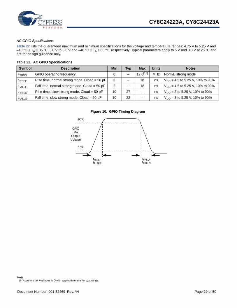
Figure 10. GPIO Timing Diagram
Table 22. AC GPIO Specifications
Symbol Description Min Typ Max Units Notes
FGPIO GPIO operating frequency 0 – 12.6[16] MHz Normal strong mode
tRISEF Rise time, normal strong mode, Cload = 50 pF 3 – 18 ns VDD = 4.5 to 5.25 V, 10% to 90%
tFALLF Fall time, normal strong mode, Cload = 50 pF 2 – 18 ns VDD = 4.5 to 5.25 V, 10% to 90%
tRISES Rise time, slow strong mode, Cload = 50 pF 10 27 – ns VDD = 3 to 5.25 V, 10% to 90%
tFALLS Fall time, slow strong mode, Cload = 50 pF 10 22 – ns VDD = 3 to 5.25 V, 10% to 90%
Note16. Accuracy derived from IMO with appropriate trim for VDD range.
TFallFTFallS
TRiseFTRiseS
90%
10%
GPIOPin
OutputVoltage
tRISEFtRISES
tFALLFtFALLS
CY8C24223A, CY8C24423A
Document Number: 001-52469 Rev. *H Page 30 of 50
AC Operational Amplifier Specifications
The following tables list the guaranteed maximum and minimum specifications for the voltage and temperature ranges: 4.75 V to 5.25 V and –40 °C TA 85 °C, 3.0 V to 3.6 V and –40 °C TA 85 °C, respectively. Typical parameters apply to 5 V and 3.3 V at 25 °C and are for design guidance only.
Settling times, slew rates, and gain bandwidth are based on the analog CT PSoC block.
Power = high and Opamp bias = high is not allowed at 3.3 V.
Table 23. 5-V AC Operational Amplifier Specifications
Symbol Description Min Typ Max Units
tROA Rising settling time from 80% of V to 0.1% of V (10 pF load, unity gain)Power = low, Opamp bias = lowPower = medium, Opamp bias = highPower = high, Opamp bias = high
–––
–––
3.90.720.62
sss
tSOA Falling settling time from 20% of V to 0.1% of V (10 pF load, unity gain)Power = low, Opamp bias = lowPower = medium, Opamp bias = highPower = high, Opamp bias = high
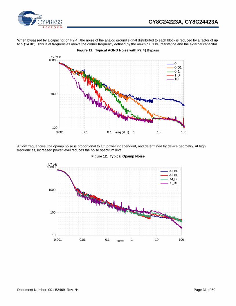
When bypassed by a capacitor on P2[4], the noise of the analog ground signal distributed to each block is reduced by a factor of up to 5 (14 dB). This is at frequencies above the corner frequency defined by the on-chip 8.1 k resistance and the external capacitor.
Figure 11. Typical AGND Noise with P2[4] Bypass
At low frequencies, the opamp noise is proportional to 1/f, power independent, and determined by device geometry. At high frequencies, increased power level reduces the noise spectrum level.
Figure 12. Typical Opamp Noise
100
1000
10000
0.001 0.01 0.1 1 10 100Freq (kHz)
nV/rtHz
00.010.11.010
10
100
1000
10000
0.001 0.01 0.1 1 10 100Freq (kHz)
nV/rtHz
PH_BHPH_BLPM_BLPL_BL
CY8C24223A, CY8C24423A
Document Number: 001-52469 Rev. *H Page 32 of 50
AC Low Power Comparator Specifications
Table 25 lists the guaranteed maximum and minimum specifications for the voltage and temperature ranges: 4.75 V to 5.25 V and –40 °C TA 85 °C, 3.0 V to 3.6 V and –40 °C TA 85 °C, respectively. Typical parameters apply to 5 V and 3.3 V at 25 °C and are for design guidance only.
AC Digital Block Specifications
Table 26 lists the guaranteed maximum and minimum specifications for the voltage and temperature ranges: 4.75 V to 5.25 V and –40 °C TA 85 °C, 3.0 V to 3.6 V and –40 °C TA 85 °C, respectively. Typical parameters apply to 5 V and 3.3 V at 25 °C and are for design guidance only.
Table 25. AC Low Power Comparator Specifications
Symbol Description Min Typ Max Units NotestRLPC LPC response time – – 50 s 50 mV overdrive comparator
reference set within VREFLPC
Table 26. AC Digital Block Specifications
Function Description Min Typ Max Units NotesAll functions Block input clock frequency
VDD 4.75 V – – 50.4[18] MHz VDD < 4.75 V – – 25.2[18] MHz
Timer Input clock frequency No capture, VDD 4.75 V – – 50.4[18] MHz No capture, VDD < 4.75 V – – 25.2[18] MHz With capture – – 25.2[18] MHzCapture pulse width 50[17] – – ns
Counter Input clock frequency No enable input, VDD 4.75 V – – 50.4[18] MHz No enable input, VDD < 4.75 V – – 25.2[18] MHz With enable input – – 25.2[18] MHzEnable input pulse width 50[17] – – ns
Dead Band Kill pulse width Asynchronous restart mode 20 – – ns Synchronous restart mode 50[17] – – ns Disable mode 50[17] – – nsInput clock frequency VDD 4.75 V – – 50.4[18] MHz VDD < 4.75 V – – 25.2[18] MHz
CRCPRS(PRS Mode)
Input clock frequency VDD 4.75 V – – 50.4[18] MHz VDD < 4.75 V – – 25.2[18] MHz
CRCPRS(CRC Mode)
Input clock frequency – – 25.2[18] MHz
SPIM Input clock frequency – – 8.4[18] MHz The SPI serial clock (SCLK) frequency is equal to the input clock frequency divided by 2.
SPIS Input clock (SCLK) frequency – – 4.2[18] MHz The input clock is the SPI SCLK in SPIS mode.
Width of SS_Negated between transmissions 50[17] – – nsTransmitter Input clock frequency The baud rate is equal to the input
clock frequency divided by 8. VDD 4.75 V, 2 stop bits – – 50.4[18] MHz VDD 4.75 V, 1 stop bit – – 25.2[18] MHz VDD < 4.75 V – – 25.2[18] MHz
Receiver Input clock frequency The baud rate is equal to the input clock frequency divided by 8. VDD 4.75 V, 2 stop bits – – 50.4[18] MHz
VDD 4.75 V, 1 stop bit – – 25.2[18] MHz VDD < 4.75 V – – 25.2[18] MHz
Notes17. 50 ns minimum input pulse width is based on the input synchronizers running at 24 MHz (42 ns nominal period).18. Accuracy derived from IMO with appropriate trim for VDD range.
CY8C24223A, CY8C24423A
Document Number: 001-52469 Rev. *H Page 33 of 50
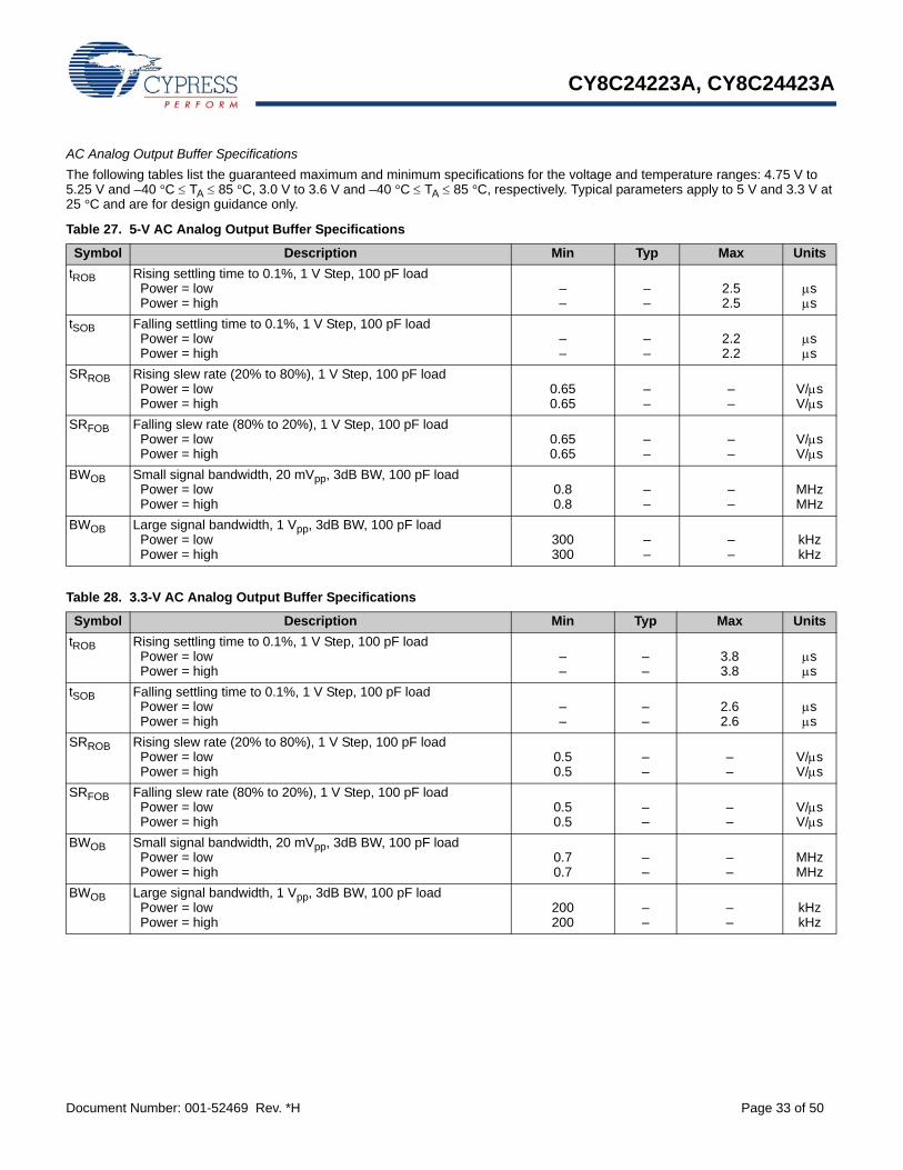
AC Analog Output Buffer Specifications
The following tables list the guaranteed maximum and minimum specifications for the voltage and temperature ranges: 4.75 V to 5.25 V and –40 °C TA 85 °C, 3.0 V to 3.6 V and –40 °C TA 85 °C, respectively. Typical parameters apply to 5 V and 3.3 V at 25 °C and are for design guidance only.
Table 27. 5-V AC Analog Output Buffer Specifications
Symbol Description Min Typ Max Units
tROB Rising settling time to 0.1%, 1 V Step, 100 pF load Power = low Power = high
––
––
2.52.5
ss
tSOB Falling settling time to 0.1%, 1 V Step, 100 pF load Power = low Power = high
––
––
2.22.2
ss
SRROB Rising slew rate (20% to 80%), 1 V Step, 100 pF load Power = low Power = high
0.650.65
––
––
V/sV/s
SRFOB Falling slew rate (80% to 20%), 1 V Step, 100 pF load Power = low Power = high
0.650.65
––
––
V/sV/s
BWOB Small signal bandwidth, 20 mVpp, 3dB BW, 100 pF load Power = low Power = high
0.80.8
––
––
MHzMHz
BWOB Large signal bandwidth, 1 Vpp, 3dB BW, 100 pF load Power = low Power = high
300300
––
––
kHzkHz
Table 28. 3.3-V AC Analog Output Buffer Specifications
Symbol Description Min Typ Max Units
tROB Rising settling time to 0.1%, 1 V Step, 100 pF load Power = low Power = high
––
––
3.83.8
ss
tSOB Falling settling time to 0.1%, 1 V Step, 100 pF load Power = low Power = high
––
––
2.62.6
ss
SRROB Rising slew rate (20% to 80%), 1 V Step, 100 pF load Power = low Power = high
0.50.5
––
––
V/sV/s
SRFOB Falling slew rate (80% to 20%), 1 V Step, 100 pF load Power = low Power = high
0.50.5
––
––
V/sV/s
BWOB Small signal bandwidth, 20 mVpp, 3dB BW, 100 pF load Power = low Power = high
0.70.7
––
––
MHzMHz
BWOB Large signal bandwidth, 1 Vpp, 3dB BW, 100 pF load Power = low Power = high
200200
––
––
kHzkHz
CY8C24223A, CY8C24423A
Document Number: 001-52469 Rev. *H Page 34 of 50
AC External Clock Specifications
The following tables list the guaranteed maximum and minimum specifications for the voltage and temperature ranges: 4.75 V to 5.25 V and –40 °C TA 85 °C, 3.0 V to 3.6 V and –40 °C TA 85 °C, respectively. Typical parameters apply to 5 V and 3.3 V at 25 °C and are for design guidance only.
AC Programming Specifications
Table 31 lists the guaranteed maximum and minimum specifications for the voltage and temperature ranges: 4.75 V to 5.25 V and –40 °C TA 85 °C, 3.0 V to 3.6 V and –40 °C TA 85 °C, respectively. Typical parameters apply to 5 V and 3.3 V at 25 °C and are for design guidance only.
Table 29. 5 V AC External Clock Specifications
Symbol Description Min Typ Max Units
FOSCEXT Frequency 0.093 – 24.6 MHz
– High period 20.6 – 5300 ns
– Low period 20.6 – – ns
– Power-up IMO to switch 150 – – s
Notes19. Maximum CPU frequency is 12 MHz nominal at 3.3 V. With the CPU clock divider set to 1, the external clock must adhere to the maximum frequency and duty cycle
requirements.20. If the frequency of the external clock is greater than 12 MHz, the CPU clock divider must be set to 2 or greater. In this case, the CPU clock divider ensures that the
fifty percent duty cycle requirement is met.21. For the full temperature range, the user must employ a temperature sensor user module (FlashTemp) or other temperature sensor, and feed the result to the
temperature argument before writing. Refer to the Flash APIs Application Note AN2015 for more information.
Table 30. 3.3 V AC External Clock Specifications
Symbol Description Min Typ Max Units
FOSCEXT Frequency with CPU clock divide by 1[19] 0.093 – 12.3 MHz
FOSCEXT Frequency with CPU clock divide by 2 or greater[20] 0.186 – 24.6 MHz
– High period with CPU clock divide by 1 41.7 – 5300 ns
– Low period with CPU clock divide by 1 41.7 – – ns
– Power-up IMO to switch 150 – – s
Table 31. AC Programming Specifications
Symbol Description Min Typ Max Units Notes
tRSCLK Rise time of SCLK 1 – 20 ns
tFSCLK Fall time of SCLK 1 – 20 ns
tSSCLK Data setup time to falling edge of SCLK 40 – – ns
tHSCLK Data hold time from falling edge of SCLK 40 – – ns
FSCLK Frequency of SCLK 0 – 8 MHz
tERASEB Flash erase time per block – 20 80[21] ms
tWRITE Flash block write time – 80 320[21] ms
tDSCLK Data out delay from falling edge of SCLK – – 45 ns VDD 3.6
tDSCLK3 Data out delay from falling edge of SCLK – – 50 ns 3.0 VDD 3.6
tERASEALL Flash erase time (bulk) – 20 – ms Erase all blocks and protection fields at once
tPRGH Total flash block program time (tERASEB + tWRITE), hot
– – 200[21] ms TJ 0 °C
tPRGC Total flash block program time (tERASEB + tWRITE), cold
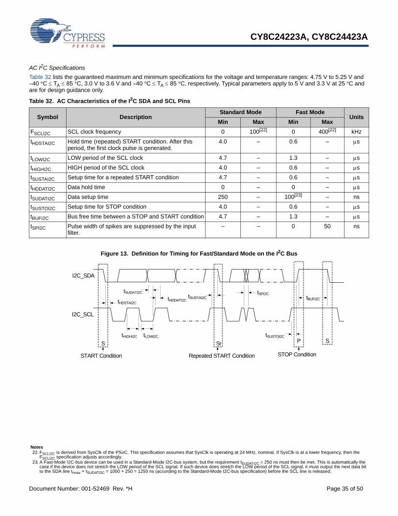
Table 32 lists the guaranteed maximum and minimum specifications for the voltage and temperature ranges: 4.75 V to 5.25 V and –40 °C TA 85 °C, 3.0 V to 3.6 V and –40 °C TA 85 °C, respectively. Typical parameters apply to 5 V and 3.3 V at 25 °C and are for design guidance only.
Figure 13. Definition for Timing for Fast/Standard Mode on the I2C Bus
Table 32. AC Characteristics of the I2C SDA and SCL Pins
Symbol DescriptionStandard Mode Fast Mode
UnitsMin Max Min Max
FSCLI2C SCL clock frequency 0 100[22] 0 400[22] kHz
tHDSTAI2C Hold time (repeated) START condition. After this period, the first clock pulse is generated.
4.0 – 0.6 – s
tLOWI2C LOW period of the SCL clock 4.7 – 1.3 – s
tHIGHI2C HIGH period of the SCL clock 4.0 – 0.6 – s
tSUSTAI2C Setup time for a repeated START condition 4.7 – 0.6 – s
tHDDATI2C Data hold time 0 – 0 – s
tSUDATI2C Data setup time 250 – 100[23] – ns
tSUSTOI2C Setup time for STOP condition 4.0 – 0.6 – s
tBUFI2C Bus free time between a STOP and START condition 4.7 – 1.3 – s
tSPI2C Pulse width of spikes are suppressed by the input filter.
– – 0 50 ns
Notes22. FSCLI2C is derived from SysClk of the PSoC. This specification assumes that SysClk is operating at 24 MHz, nominal. If SysClk is at a lower frequency, then the
FSCLI2C specification adjusts accordingly.23. A Fast-Mode I2C-bus device can be used in a Standard-Mode I2C-bus system, but the requirement tSUDATI2C 250 ns must then be met. This is automatically the
case if the device does not stretch the LOW period of the SCL signal. If such device does stretch the LOW period of the SCL signal, it must output the next data bit to the SDA line trmax + tSUDATI2C = 1000 + 250 = 1250 ns (according to the Standard-Mode I2C-bus specification) before the SCL line is released.
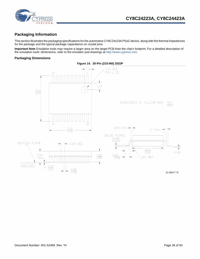
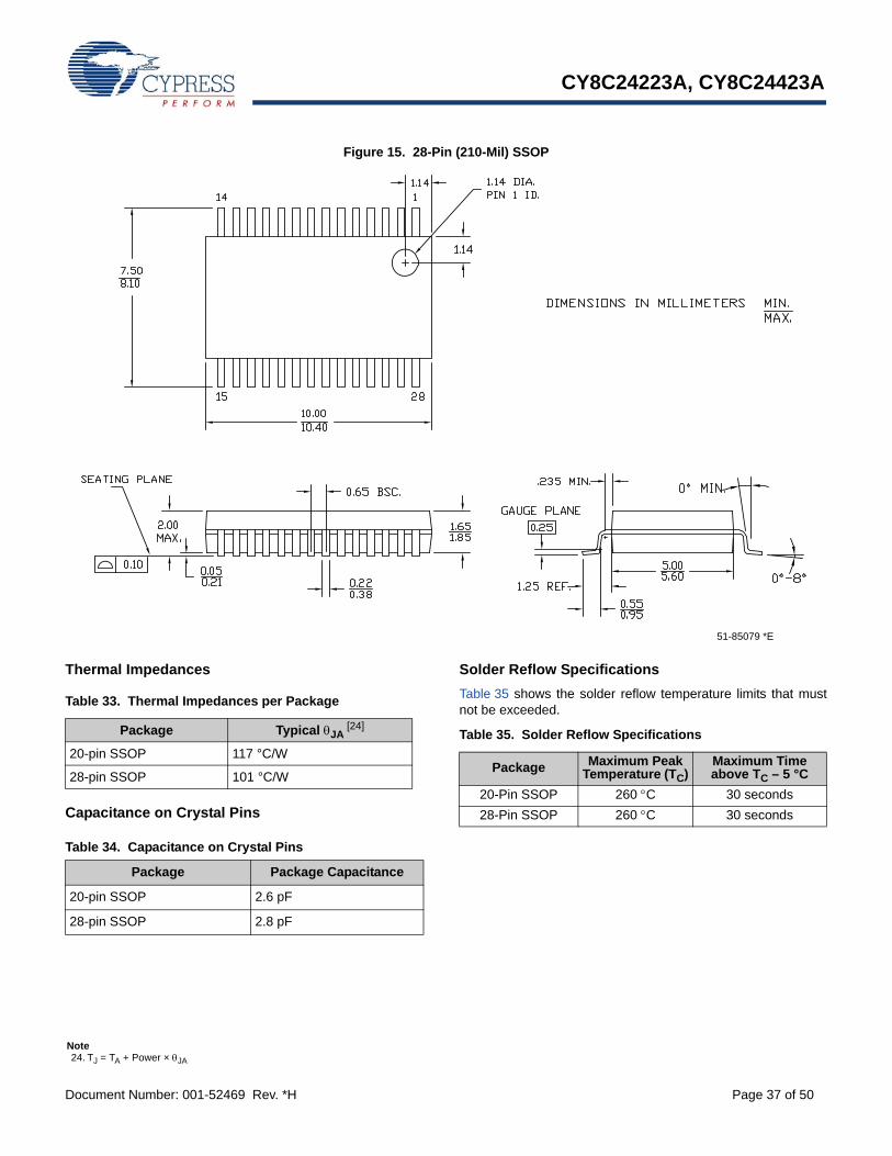
This section illustrates the packaging specifications for the automotive CY8C24x23A PSoC device, along with the thermal impedances for the package and the typical package capacitance on crystal pins.
Important Note Emulation tools may require a larger area on the target PCB than the chip’s footprint. For a detailed description of the emulation tools’ dimensions, refer to the emulator pod drawings at http://www.cypress.com.
Table 35 shows the solder reflow temperature limits that mustnot be exceeded.
51-85079 *E
Table 33. Thermal Impedances per Package
Package Typical JA [24]
20-pin SSOP 117 °C/W
28-pin SSOP 101 °C/W
Table 34. Capacitance on Crystal Pins
Package Package Capacitance
20-pin SSOP 2.6 pF
28-pin SSOP 2.8 pF
Table 35. Solder Reflow Specifications
Package Maximum Peak Temperature (TC)
Maximum Time above TC – 5 °C
20-Pin SSOP 260 C 30 seconds
28-Pin SSOP 260 C 30 seconds
Note24. TJ = TA + Power × JA
CY8C24223A, CY8C24423A
Document Number: 001-52469 Rev. *H Page 38 of 50
Figure 16. 20-Pin SSOP Carrier Tape Drawing
51-51101 *C
CY8C24223A, CY8C24423A
Document Number: 001-52469 Rev. *H Page 39 of 50
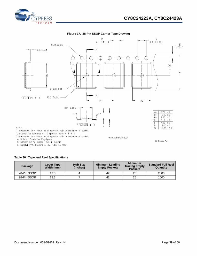
Figure 17. 28-Pin SSOP Carrier Tape Drawing
51-51100 *C
Table 36. Tape and Reel Specifications
Package Cover Tape Width (mm)
Hub Size(inches)
Minimum Leading Empty Pockets
MinimumTrailing Empty
Pockets
Standard Full Reel Quantity
20-Pin SSOP 13.3 4 42 25 2000
28-Pin SSOP 13.3 7 42 25 1000
CY8C24223A, CY8C24423A
Document Number: 001-52469 Rev. *H Page 40 of 50
Development Tool Selection
This section presents the development tools available for the CY8C24x23A family.
Software
PSoC DesignerAt the core of the PSoC development software suite is PSoC Designer, used to generate PSoC firmware applications. PSoC Designer is available free of charge at http://www.cypress.com and includes a free C compiler.
PSoC Programmer
Flexible enough to be used on the bench in development, yet suitable for factory programming, PSoC Programmer works either as a standalone programming application or it can operate directly from PSoC Designer or PSoC Express. PSoC Programmer software is compatible with both PSoC ICE-Cube In-Circuit Emulator and PSoC MiniProg. PSoC programmer is available free of charge at http://www.cypress.com.
Development Kits
All development kits can be purchased from the Cypress Online Store. The online store also has the most up to date information on kit contents, descriptions, and availability.
CY3215-DK Basic Development Kit
The CY3215-DK is for prototyping and development with PSoC Designer. This kit supports in-circuit emulation and the software interface allows users to run, halt, and single step the processor and view the contents of specific memory locations. Advanced emulation features are also supported through PSoC Designer. The kit includes:
■ MiniEval socket programming and evaluation board
■ Backward compatibility cable (for connecting to legacy pods)
■ Universal 110/220 power supply (12 V)
■ European plug adapter
■ USB 2.0 cable
■ Getting Started guide
■ Development kit registration form
Evaluation Tools
All evaluation tools can be purchased from the Cypress Online Store.
CY3210-PSoCEval1
The CY3210-PSoCEval1 kit features an evaluation board and the MiniProg1 programming unit. The evaluation board includes an LCD module, potentiometer, LEDs, an RS-232 port, and plenty of breadboarding space to meet all of your evaluation needs. The kit includes:
PSoC EvalPods are pods that connect to the ICE (CY3215-DK kit) to allow debugging capability. They can also function as a standalone device without debugging capability. The EvalPod has a 28-pin DIP footprint on the bottom for easy connection to development kits or other hardware. The top of the EvalPod has prototyping headers for easy connection to the device's pins. CY3210-24X23 provides evaluation of the CY8C24x23A PSoC device family.
Device Programmers
All device programmers can be purchased from the Cypress Online Store.
CY3210-MiniProg1
The CY3210-MiniProg1 kit allows a user to program PSoC devices via the MiniProg1 programming unit. The MiniProg is a small, compact prototyping programmer that connects to the PC via a provided USB 2.0 cable. The kit includes:
■ MiniProg programming unit
■ MiniEval socket programming and evaluation board
■ 28-pin CY8C29466-24PXI PDIP PSoC device sample
■ PSoC Designer software CD
■ Getting Started guide
■ USB 2.0 cable
CY3207ISSP In-System Serial Programmer (ISSP)
The CY3207ISSP is a production programmer. It includes protection circuitry and an industrial case that is more robust than the MiniProg in a production-programming environment.
Note CY3207ISSP needs special software and is not compatible with PSoC Programmer. This software is free and can be downloaded from http://www.cypress.com. The kit includes:
■ CY3207 programmer unit
■ PSoC ISSP software CD
■ 110 ~ 240-V power supply, Euro-Plug adapter
■ USB 2.0 cable
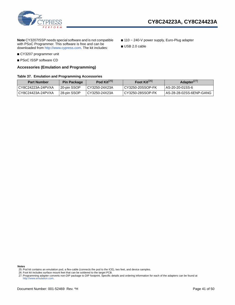
Accessories (Emulation and Programming)
Table 37. Emulation and Programming Accessories
Part Number Pin Package Pod Kit[25] Foot Kit[26] Adapter[27]
Notes25. Pod kit contains an emulation pod, a flex-cable (connects the pod to the ICE), two feet, and device samples.26. Foot kit includes surface mount feet that can be soldered to the target PCB.27. Programming adapter converts non-DIP package to DIP footprint. Specific details and ordering information for each of the adapters can be found at
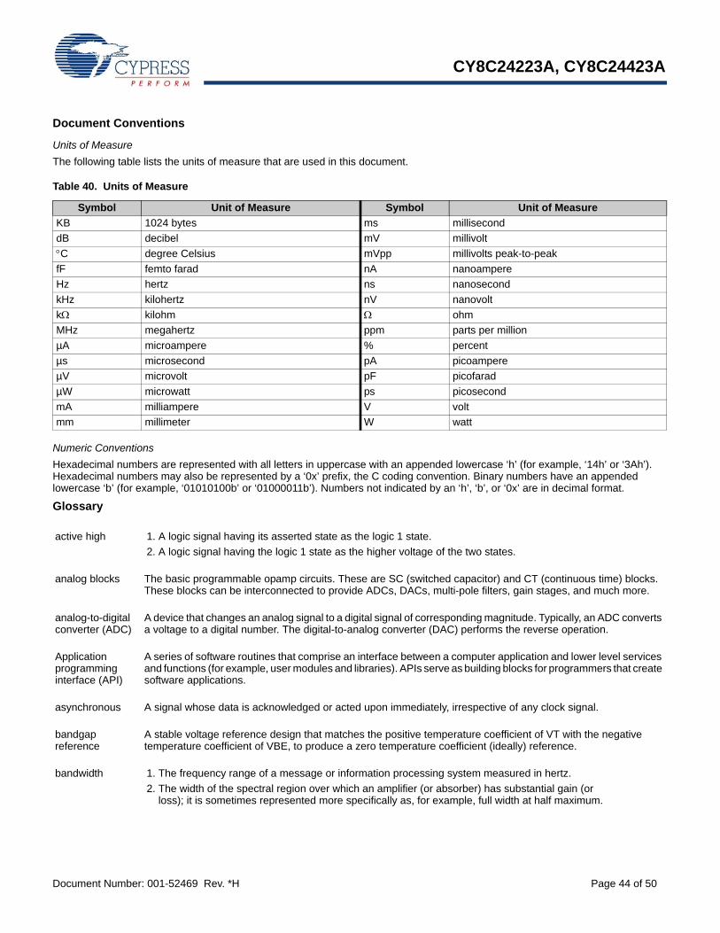
The following table lists the units of measure that are used in this document.
Numeric Conventions
Hexadecimal numbers are represented with all letters in uppercase with an appended lowercase ‘h’ (for example, ‘14h’ or ‘3Ah’). Hexadecimal numbers may also be represented by a ‘0x’ prefix, the C coding convention. Binary numbers have an appended lowercase ‘b’ (for example, ‘01010100b’ or ‘01000011b’). Numbers not indicated by an ‘h’, ‘b’, or ‘0x’ are in decimal format.
Table 40. Units of Measure
Symbol Unit of Measure Symbol Unit of Measure
KB 1024 bytes ms millisecond
dB decibel mV millivolt
C degree Celsius mVpp millivolts peak-to-peak
fF femto farad nA nanoampere
Hz hertz ns nanosecond
kHz kilohertz nV nanovolt
k kilohm ohm
MHz megahertz ppm parts per million
µA microampere % percent
µs microsecond pA picoampere
µV microvolt pF picofarad
µW microwatt ps picosecond
mA milliampere V volt
mm millimeter W watt
Glossary
active high 1. A logic signal having its asserted state as the logic 1 state.
2. A logic signal having the logic 1 state as the higher voltage of the two states.
analog blocks The basic programmable opamp circuits. These are SC (switched capacitor) and CT (continuous time) blocks. These blocks can be interconnected to provide ADCs, DACs, multi-pole filters, gain stages, and much more.
analog-to-digital converter (ADC)
A device that changes an analog signal to a digital signal of corresponding magnitude. Typically, an ADC converts a voltage to a digital number. The digital-to-analog converter (DAC) performs the reverse operation.
Application programming interface (API)
A series of software routines that comprise an interface between a computer application and lower level services and functions (for example, user modules and libraries). APIs serve as building blocks for programmers that create software applications.
asynchronous A signal whose data is acknowledged or acted upon immediately, irrespective of any clock signal.
bandgap reference
A stable voltage reference design that matches the positive temperature coefficient of VT with the negative temperature coefficient of VBE, to produce a zero temperature coefficient (ideally) reference.
bandwidth 1. The frequency range of a message or information processing system measured in hertz.
2. The width of the spectral region over which an amplifier (or absorber) has substantial gain (orloss); it is sometimes represented more specifically as, for example, full width at half maximum.
CY8C24223A, CY8C24423A
Document Number: 001-52469 Rev. *H Page 45 of 50
bias 1. A systematic deviation of a value from a reference value.
2. The amount by which the average of a set of values departs from a reference value.
3. The electrical, mechanical, magnetic, or other force (field) applied to a device to establish a reference level to operate the device.
block 1. A functional unit that performs a single function, such as an oscillator.
2. A functional unit that may be configured to perform one of several functions, such as a digital PSoC block or an analog PSoC block.
buffer 1. A storage area for data that is used to compensate for a speed difference, when transferring data from one device to another. Usually refers to an area reserved for I/O operations, into which data is read, or from which data is written.
2. A portion of memory set aside to store data, often before it is sent to an external device or as it is received from an external device.
3. An amplifier used to lower the output impedance of a system.
bus 1. A named connection of nets. Bundling nets together in a bus makes it easier to route nets with similar routing patterns.
2. A set of signals performing a common function and carrying similar data. Typically represented using vector notation; for example, address[7:0].
3. One or more conductors that serve as a common connection for a group of related devices.
clock The device that generates a periodic signal with a fixed frequency and duty cycle. A clock is sometimes used to synchronize different logic blocks.
comparator An electronic circuit that produces an output voltage or current whenever two input levels simultaneously satisfy predetermined amplitude requirements.
compiler A program that translates a high level language, such as C, into machine language.
configuration space
In PSoC devices, the register space accessed when the XIO bit, in the CPU_F register, is set to‘1’.
crystal oscillator An oscillator in which the frequency is controlled by a piezoelectric crystal. Typically a piezoelectriccrystal is less sensitive to ambient temperature than other circuit components.
cyclic redundancy check (CRC)
A calculation used to detect errors in data communications, typically performed using a linear feedback shift register. Similar calculations may be used for a variety of other purposes such as data compression.
data bus A bi-directional set of signals used by a computer to convey information from a memory location to the central processing unit and vice versa. More generally, a set of signals used to convey data between digital functions.
debugger A hardware and software system that allows you to analyze the operation of the system under development. A debugger usually allows the developer to step through the firmware one step at a time, set break points, and analyze memory.
dead band A period of time when neither of two or more signals are in their active state or in transition.
digital blocks The 8-bit logic blocks that can act as a counter, timer, serial receiver, serial transmitter, CRC generator, pseudo-random number generator, or SPI.
digital-to-analog converter (DAC)
A device that changes a digital signal to an analog signal of corresponding magnitude. The analog-to-digital converter (ADC) performs the reverse operation.
Glossary (continued)
CY8C24223A, CY8C24423A
Document Number: 001-52469 Rev. *H Page 46 of 50
duty cycle The relationship of a clock period high time to its low time, expressed as a percent.
emulator Duplicates (provides an emulation of) the functions of one system with a different system, so that the second system appears to behave like the first system.
external reset (XRES)
An active high signal that is driven into the PSoC device. It causes all operation of the CPU and blocks to stop and return to a pre-defined state.
flash An electrically programmable and erasable, non-volatile technology that provides you the programmability and data storage of EPROMs, plus in-system erasability. Non-volatile means that the data is retained when power is off.
flash block The smallest amount of flash ROM space that may be programmed at one time and the smallest amount of flash space that may be protected.
frequency The number of cycles or events per unit of time, for a periodic function.
gain The ratio of output current, voltage, or power to input current, voltage, or power, respectively. Gain is usually expressed in dB.
I2C A two-wire serial computer bus by Philips Semiconductors (now NXP Semiconductors). It is used to connect low-speed peripherals in an embedded system. The original system was created in the early 1980s as a battery control interface, but it was later used as a simple internal bus system for building control electronics. I2C uses only two bi-directional pins, clock and data, both running at the VDD supply voltage and pulled high with resistors. The bus operates up to100 kbits/second in standard mode and 400 kbits/second in fast mode.
ICE The in-circuit emulator that allows you to test the project in a hardware environment, while viewing the debugging device activity in a software environment (PSoC Designer).
input/output (I/O) A device that introduces data into or extracts data from a system.
interrupt A suspension of a process, such as the execution of a computer program, caused by an event external to that process, and performed in such a way that the process can be resumed.
interrupt service routine (ISR)
A block of code that normal code execution is diverted to when the CPU receives a hardware interrupt. Many interrupt sources may each exist with its own priority and individual ISR code block. Each ISR code block ends with the RETI instruction, returning the device to the point in the program where it left normal program execution.
jitter 1. A misplacement of the timing of a transition from its ideal position. A typical form of corruption that occurs on serial data streams.
2. The abrupt and unwanted variations of one or more signal characteristics, such as the interval between successive pulses, the amplitude of successive cycles, or the frequency or phase of successive cycles.
low voltage detect (LVD)
A circuit that senses VDD and provides an interrupt to the system when VDD falls below a selected threshold.
M8C An 8-bit Harvard-architecture microprocessor. The microprocessor coordinates all activity inside a PSoC by interfacing to the flash, SRAM, and register space.
master device A device that controls the timing for data exchanges between two devices. Or when devices are cascaded in width, the master device is the one that controls the timing for data exchanges between the cascaded devices and an external interface. The controlled device is called the slave device.
Glossary (continued)
CY8C24223A, CY8C24423A
Document Number: 001-52469 Rev. *H Page 47 of 50
microcontroller An integrated circuit chip that is designed primarily for control systems and products. In addition to a CPU, a microcontroller typically includes memory, timing circuits, and I/O circuitry. The reason for this is to permit the realization of a controller with a minimal quantity of chips, thus achieving maximal possible miniaturization. This in turn, reduces the volume and the cost of the controller. The microcontroller is normally not used for general-purpose computation as is a microprocessor.
mixed-signal The reference to a circuit containing both analog and digital techniques and components.
modulator A device that imposes a signal on a carrier.
noise 1. A disturbance that affects a signal and that may distort the information carried by the signal.
2. The random variations of one or more characteristics of any entity such as voltage, current, or data.
oscillator A circuit that may be crystal controlled and is used to generate a clock frequency.
parity A technique for testing transmitted data. Typically, a binary digit is added to the data to make the sum of all the digits of the binary data either always even (even parity) or always odd (odd parity).
phase-locked loop (PLL)
An electronic circuit that controls an oscillator so that it maintains a constant phase angle relative to a reference signal.
pinouts The pin number assignment: the relation between the logical inputs and outputs of the PSoC device and their physical counterparts in the printed circuit board (PCB) package. Pinouts involve pin numbers as a link between schematic and PCB design (both being computer generated files) and may also involve pin names.
port A group of pins, usually eight.
power-on reset (POR)
A circuit that forces the PSoC device to reset when the voltage is below a pre-set level. This is one type of hardware reset.
PSoC® Cypress Semiconductor’s PSoC® is a registered trademark and Programmable System-on-Chip™ is a trademark of Cypress.
PSoC Designer™ The software for Cypress’ Programmable System-on-Chip technology.
pulse width modulator (PWM)
An output in the form of duty cycle which varies as a function of the applied value.
RAM An acronym for random access memory. A data-storage device from which data can be read out and new data can be written in.
register A storage device with a specific capacity, such as a bit or byte.
reset A means of bringing a system back to a known state. See hardware reset and software reset.
ROM An acronym for read only memory. A data-storage device from which data can be read out, but new data cannot be written in.
serial 1. Pertaining to a process in which all events occur one after the other.
2. Pertaining to the sequential or consecutive occurrence of two or more related activities in a single device or channel.
settling time The time it takes for an output signal or value to stabilize after the input has changed from one value to another.
Glossary (continued)
CY8C24223A, CY8C24423A
Document Number: 001-52469 Rev. *H Page 48 of 50
shift register A memory storage device that sequentially shifts a word either left or right to output a stream of serial data.
slave device A device that allows another device to control the timing for data exchanges between two devices. Or when devices are cascaded in width, the slave device is the one that allows another device to control the timing of data exchanges between the cascaded devices and an external interface. The controlling device is called the master device.
SRAM An acronym for static random access memory. A memory device where you can store and retrieve data at a high rate of speed. The term static is used because, after a value is loaded into an SRAM cell, it remains unchanged until it is explicitly altered or until power is removed from the device.
SROM An acronym for supervisory read only memory. The SROM holds code that is used to boot the device, calibrate circuitry, and perform flash operations. The functions of the SROM may be accessed in normal user code, operating from flash.
stop bit A signal following a character or block that prepares the receiving device to receive the next character or block.
synchronous 1. A signal whose data is not acknowledged or acted upon until the next active edge of a clock signal.
2. A system whose operation is synchronized by a clock signal.
tri-state A function whose output can adopt three states: 0, 1, and Z (high-impedance). The function does not drive any value in the Z state and, in many respects, may be considered to be disconnected from the rest of the circuit, allowing another output to drive the same net.
UART A UART or universal asynchronous receiver-transmitter translates between parallel bits of data and serial bits.
user modules Pre-built, pre-tested hardware/firmware peripheral functions that take care of managing and configuring the lower level analog and digital PSoC blocks. User modules also provide high level API (Application Programming Interface) for the peripheral function.
user space The bank 0 space of the register map. The registers in this bank are more likely to be modified during normal program execution and not just during initialization. Registers in bank 1 are most likely to be modified only during the initialization phase of the program.
VDD A name for a power net meaning "voltage drain". The most positive power supply signal. Usually 5 V or 3.3 V.
VSS A name for a power net meaning "voltage source." The most negative power supply signal.
watchdog timer A timer that must be serviced periodically. If it is not serviced, the CPU resets after a specified period of time.
** 2678061 VIVG/PYRS 03/24/09 New data sheet for Automotive A-Grade
*A 2685606 SHEA 04/08/09 Minor ECN to correct the spec number in Document History.
*B 2702925 BTK 05/06/2009 Post to external web
*C 2742354 BTK/PYRS 07/22/09 Changed title. Updated Features section. Updated text of PSoC Functional Overview section. Updated Getting Started section. Made corrections and minor text edits to Pinouts section. Changed the name of the Register Reference section to "Registers". Added clarifying comments to some electrical specifica-tions. Updated some figures. Changed TRAMP specification per MASJ input. Fixed all AC specifications to conform to a ±5% IMO accuracy. Made other miscellaneous minor text edits. Deleted some non-applicable or redundant infor-mation. Added a footnote to clarify that 8 of the 12 analog inputs are regular and the other 4 are direct SC block connections. Updated Development Tool Selection section.
*D 2822792 BTK/AESA 12/07/2009 Added TPRGH, TPRGC, IOL, IOH, F32KU, DCILO, and TPOWERUP electrical specifi-cations. Corrected the FlashENT electrical specification. Updated all footnotes for Table 20, “DC Programming Specifications,” on page 26. Added maximum values and updated typical values for TERASEB and TWRITE electrical specifica-tions. Replaced TRAMP electrical specification with SRPOWERUP electrical speci-fication. Added “Contents” on page 2.
*E 2888007 NJF 03/30/2010 Updated Cypress website links.Removed reference to PSoC Designer 4.4.Added TBAKETEMP and TBAKETIME parameters in Absolute Maximum Ratings on page 14.Updated 3.3 V DC Analog Reference Specifications on page 21.Removed Third Party Tools and Build a PSoC Emulator into Your Board.Updated links in Sales, Solutions, and Legal Information.
*F 3070556 BTK 10/25/2010 Added CY8C24223A-24PVXA(T) devices to datasheet.Updated the following sections: Getting Started, Development Tools, and Designing with PSoC DesignerMoved Acronyms and Document Conventions to the end of document.Added Reference Information and Glossary sections.Updated datasheet as per Cypress style guide and new datasheet template.
*G 3110316 BTK/NJF 05/12/11 Updated I2C timing diagram to improve clarity.Updated wording, formatting, and notes of the AC Digital Block Specifications table to improve clarity.Added VDDP, VDDLV, and VDDHV electrical specifications to give more information for programming the device.Updated solder reflow temperature specifications to give more clarity.Updated the jitter specifications.Updated PSoC Device Characteristics table.Updated the F32KU electrical specification.Updated note for RPD electrical specification.Updated note for the TSTG electrical specification to add more clarity.Added Tape and Reel Information section.Added CL electrical specification.Updated Analog Reference specifications.
*H 3980449 AESA 04/24/13 Updated Figure 16 and Figure 17.
Document Number: 001-52469 Rev. *H Revised April 24, 2013 Page 50 of 50
PSoC Designer™ and Programmable System-on-Chip™ are trademarks and PSoC® and CapSense® are registered trademarks of Cypress Semiconductor Corporation.
Purchase of I2C components from Cypress or one of its sublicensed Associated Companies conveys a license under the Philips I2C Patent Rights to use these components in an I2C system, providedthat the system conforms to the I2C Standard Specification as defined by Philips. As from October 1st, 2006 Philips Semiconductors has a new trade name - NXP Semiconductors.
All products and company names mentioned in this document may be the trademarks of their respective holders.
Any Source Code (software and/or firmware) is owned by Cypress Semiconductor Corporation (Cypress) and is protected by and subject to worldwide patent protection (United States and foreign),United States copyright laws and international treaty provisions. Cypress hereby grants to licensee a personal, non-exclusive, non-transferable license to copy, use, modify, create derivative works of,and compile the Cypress Source Code and derivative works for the sole purpose of creating custom software and or firmware in support of licensee product to be used only in conjunction with a Cypressintegrated circuit as specified in the applicable agreement. Any reproduction, modification, translation, compilation, or representation of this Source Code except as specified above is prohibited withoutthe express written permission of Cypress.
Disclaimer: CYPRESS MAKES NO WARRANTY OF ANY KIND, EXPRESS OR IMPLIED, WITH REGARD TO THIS MATERIAL, INCLUDING, BUT NOT LIMITED TO, THE IMPLIED WARRANTIESOF MERCHANTABILITY AND FITNESS FOR A PARTICULAR PURPOSE. Cypress reserves the right to make changes without further notice to the materials described herein. Cypress does notassume any liability arising out of the application or use of any product or circuit described herein. Cypress does not authorize its products for use as critical components in life-support systems wherea malfunction or failure may reasonably be expected to result in significant injury to the user. The inclusion of Cypress’ product in a life-support systems application implies that the manufacturerassumes all risk of such use and in doing so indemnifies Cypress against all charges.
Use may be limited by and subject to the applicable Cypress software license agreement.
Sales, Solutions, and Legal Information
Worldwide Sales and Design Support
Cypress maintains a worldwide network of offices, solution centers, manufacturer’s representatives, and distributors. To find the office closest to you, visit us at Cypress Locations.