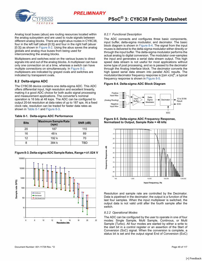
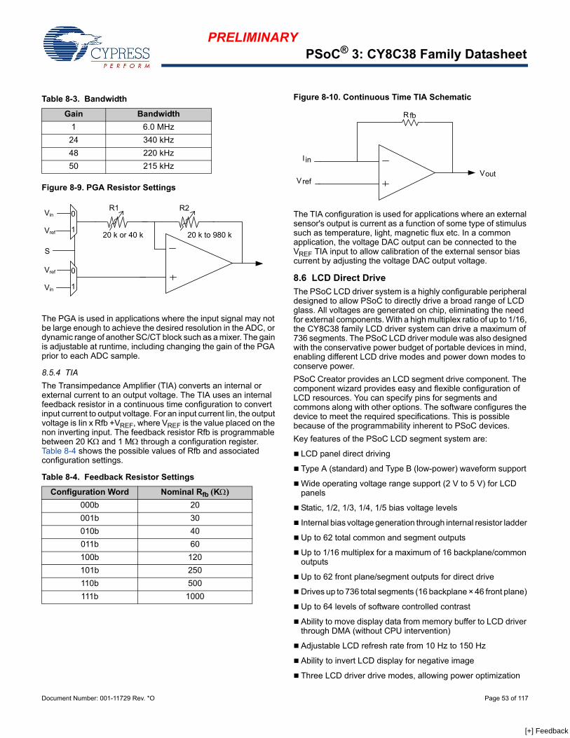
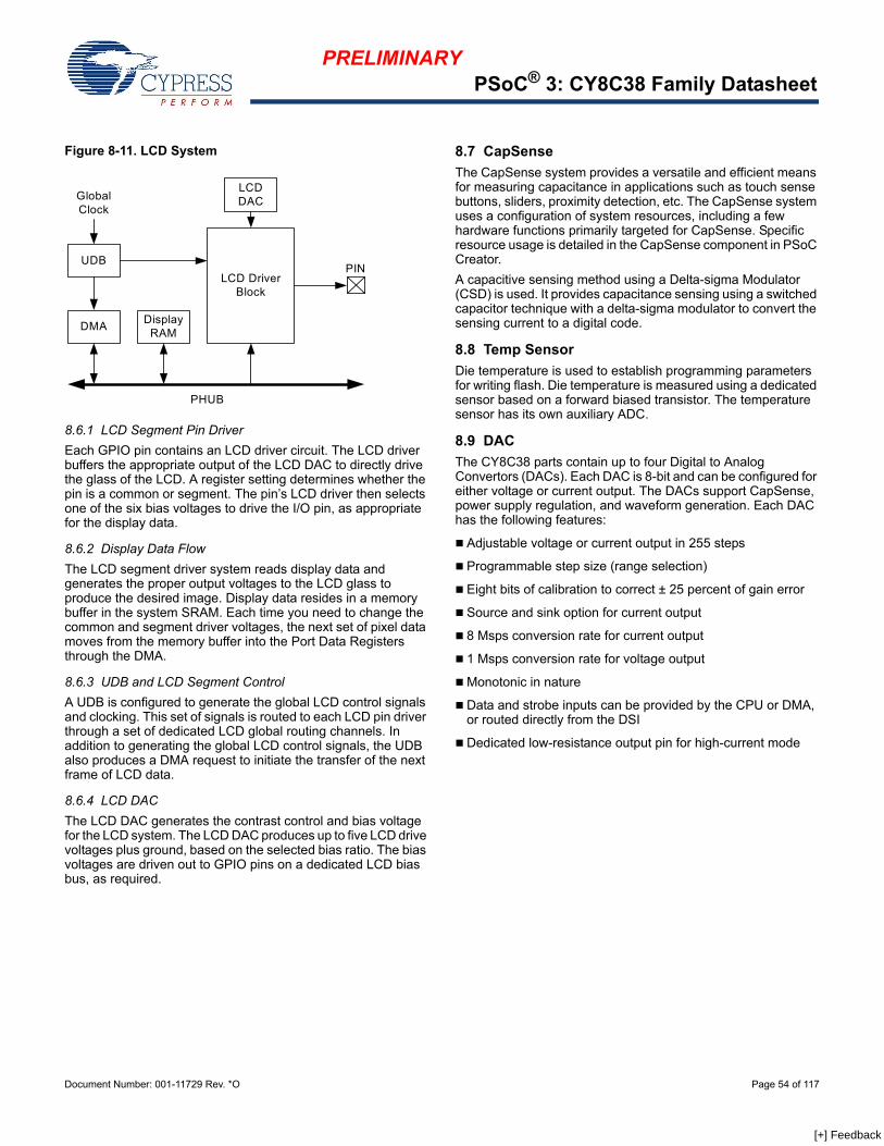
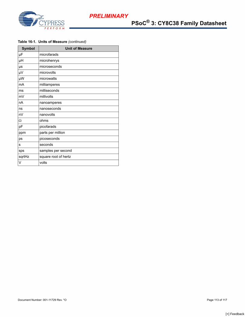
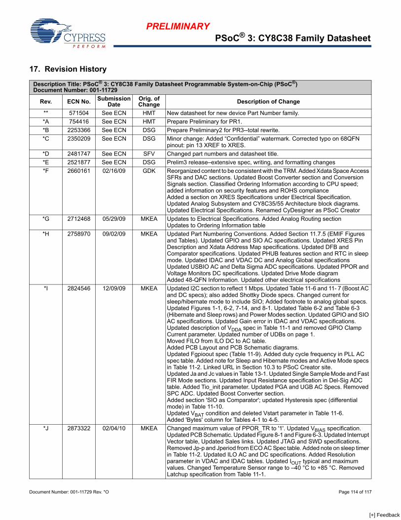
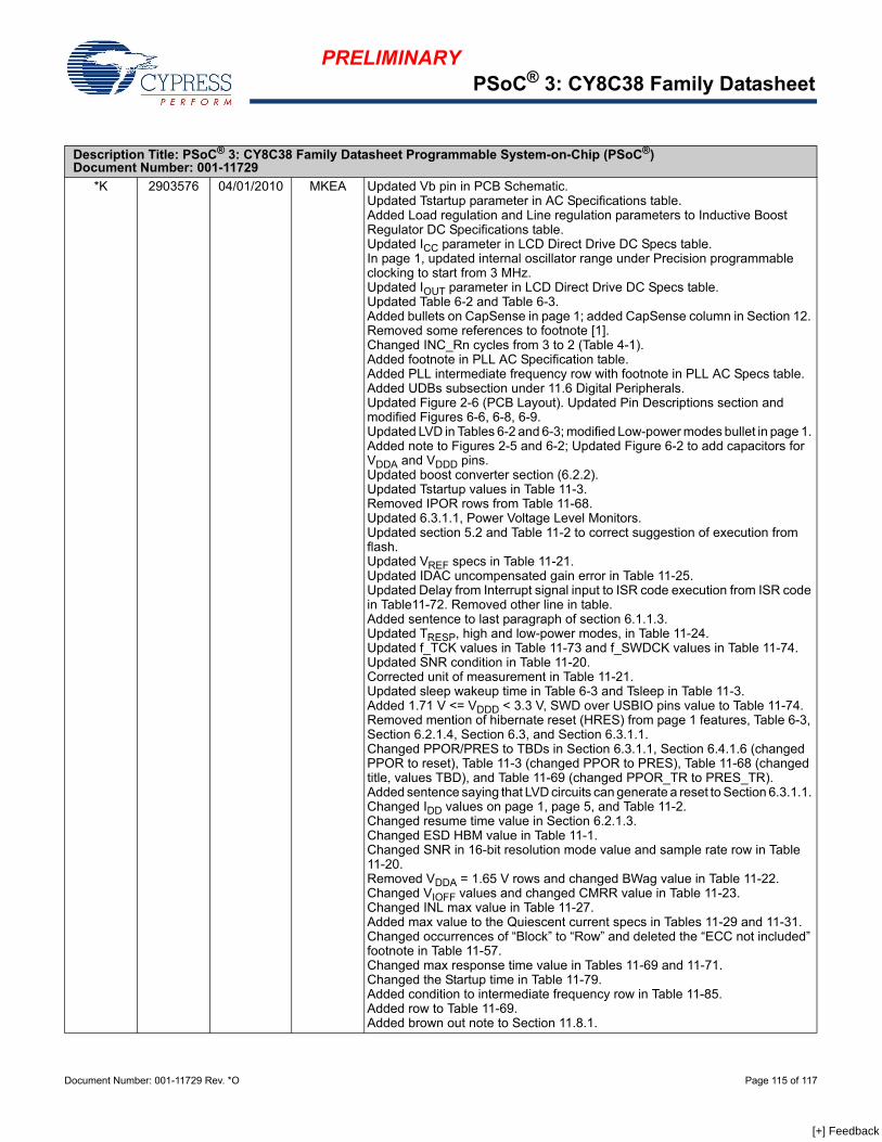
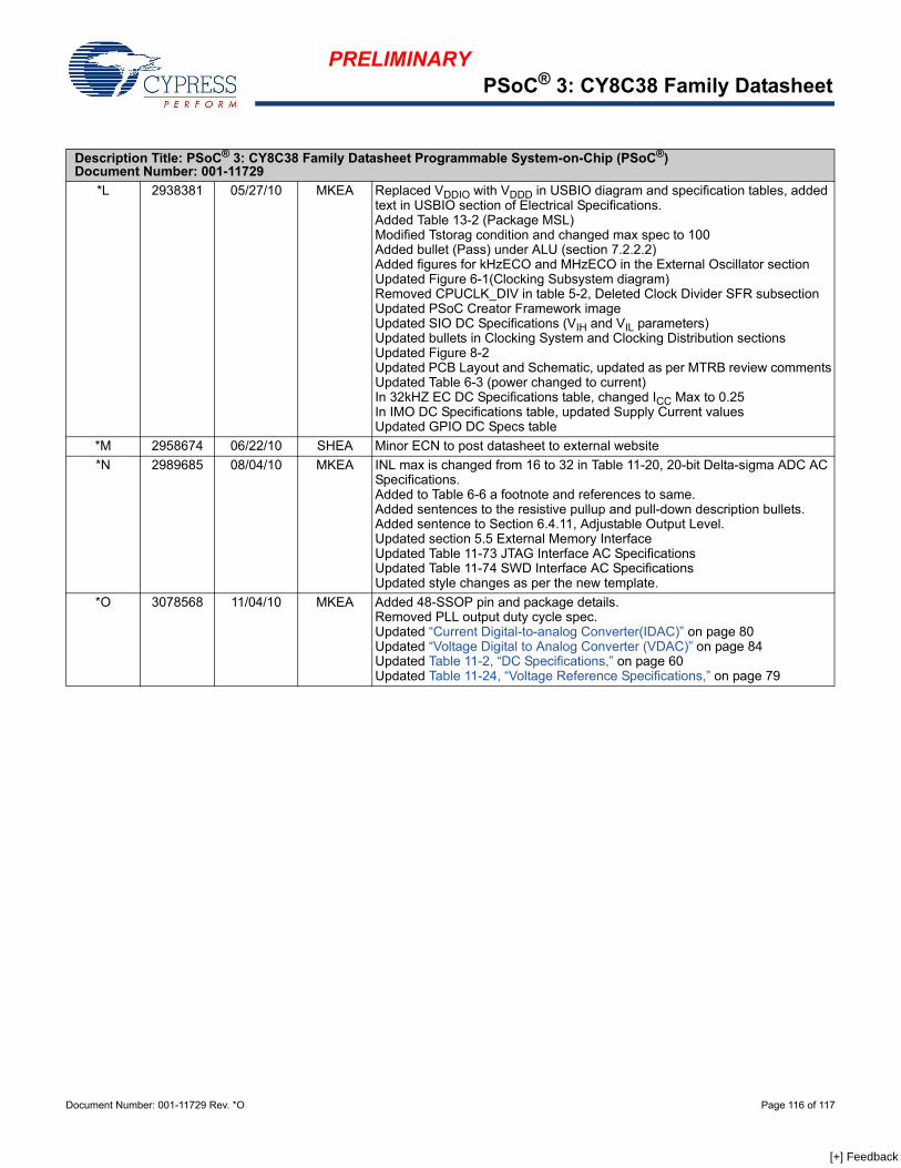
PRELIMINARY PSoC ® 3: CY8C38 Family Datasheet Programmable System-on-Chip (PSoC ® ) Cypress Semiconductor Corporation • 198 Champion Court • San Jose, CA 95134-1709 • 408-943-2600 Document Number: 001-11729 Rev. *O Revised November 4, 2010 General Description With its unique array of configurable blocks, PSoC ® 3 is a true system level solution providing microcontroller unit (MCU), memory, analog, and digital peripheral functions in a single chip. The CY8C38 family offers a modern method of signal acquisition, signal processing, and control with high accuracy, high bandwidth, and high flexibility. Analog capability spans the range from thermocouples (near DC voltages) to ultrasonic signals. The CY8C38 family can handle dozens of data acquisition channels and analog inputs on every general-purpose input/output (GPIO) pin. The CY8C38 family is also a high-performance configurable digital system with some part numbers including interfaces such as USB, multimaster inter-integrated circuit (I 2 C), and controller area network (CAN). In addition to communication interfaces, the CY8C38 family has an easy to configure logic array, flexible routing to all I/O pins, and a high-performance single cycle 8051 microprocessor core. You can easily create system-level designs using a rich library of prebuilt components and boolean primitives using PSoC Creator™, a hierarchical schematic design entry tool. The CY8C38 family provides unparalleled opportunities for analog and digital bill of materials integration while easily accommodating last minute design changes through simple firmware updates. Features Single cycle 8051 CPU DC to 67 MHz operation Multiply and divide instructions Flash program memory, up to 64 KB, 100,000 write cycles, 20 years retention, and multiple security features Up to 8-KB flash error correcting code (ECC) or configuration storage Up to 8 KB SRAM Up to 2 KB electrically erasable programmable read-only memory (EEPROM), 1 M cycles, and 20 years retention 24-channel direct memory access (DMA) with multilayer AHB [1] bus access • Programmable chained descriptors and priorities • High bandwidth 32-bit transfer support Low voltage, ultra low-power Wide operating voltage range: 0.5 V to 5.5 V High efficiency boost regulator from 0.5-V input through 1.8-V to 5.0-V output 0.8 mA at 3 MHz, 1.2 mA at 6 MHz, and 6.6 mA at 48 MHz Low-power modes including: • 1-μA sleep mode with real time clock and low-voltage detect (LVD) interrupt • 200-nA hibernate mode with RAM retention Versatile I/O system 28 to 72 I/O (62 GPIOs, eight special input/outputs (SIO), two USBIOs [2] ) Any GPIO to any digital or analog peripheral routability LCD direct drive from any GPIO, up to 46 × 16 segments [2] CapSense ® support from any GPIO [3] 1.2-V to 5.5-V I/O interface voltages, up to four domains Maskable, independent IRQ on any pin or port Schmitt-trigger transistor-transistor logic (TTL) inputs All GPIO configurable as open drain high/low, pull-up/pull-down, High Z, or strong output Configurable GPIO pin state at power-on reset (POR) 25 mA sink on SIO Digital peripherals 20 to 24 programmable logic device (PLD) based universal digital blocks (UDB) Full CAN 2.0b 16 Rx, 8 Tx buffers [2] Full-speed (FS) USB 2.0 12 Mbps using internal oscillator [2] Up to four 16-bit configurable timer, counter, and PWM blocks Library of standard peripherals • 8-, 16-, 24-, and 32-bit timers, counters, and PWMs • Serial peripheral interface (SPI), universal asynchronous transmitter receiver (UART), and I 2 C • Many others available in catalog Library of advanced peripherals • Cyclic redundancy check (CRC) • Pseudo random sequence (PRS) generator • Local interconnect network (LIN) bus 2.0 • Quadrature decoder Analog peripherals (1.71 V V DDA 5.5 V) 1.024 V ± 0.1% internal voltage reference across –40 °C to +85 °C (14 ppm/°C) Configurable delta-sigma ADC with 8- to 20-bit resolution • Sample rates up to 192 ksps • Programmable gain stage: ×0.25 to ×16 • 12-bit mode, 192 ksps, 70-dB signal-to-noise ratio (SNR), ±1-bit INL/DNL • 16-bit mode, 48 ksps, 89-dB SNR, ±2-bit INL, ±1-bit DNL 67 MHz, 24-bit fixed point digital filter block (DFB) to implement FIR and IIR filters Up to four 8-bit, 8-Msps IDACs or 1-Msps VDACs Four comparators with 95-ns response time Up to four uncommitted opamps with 25-mA drive capability Up to four configurable multifunction analog blocks. Example configurations are programmable gain amplifier (PGA), transimpedance amplifier (TIA), mixer, and sample and hold CapSense support Programming, debug, and trace JTAG (4-wire), serial wire debug (SWD) (2-wire), and single wire viewer (SWV) interfaces Eight address and one data breakpoint 4-KB instruction trace buffer Bootloader programming supportable through I 2 C, SPI, UART, USB, and other interfaces Precision, programmable clocking 3- to 62-MHz internal oscillator over full temperature and voltage range 4- to 33-MHz crystal oscillator for crystal PPM accuracy Internal PLL clock generation up to 67 MHz 32.768-kHz watch crystal oscillator Low-power internal oscillator at 1, 33, and 100 kHz Temperature and packaging –40°C to +85 °C degrees industrial temperature 48-pin SSOP, 48-pin QFN, 68-pin QFN, and 100-pin TQFP package options Notes 1. AHB – AMBA (advanced microcontroller bus architecture) high-performance bus, an ARM data transfer bus 2. This feature on select devices only. See Ordering Information on page 105 for details. 3. GPIOs with opamp outputs are not recommended for use with CapSense. [+] Feedback
Transcript
PRELIMINARY
PSoC® 3: CY8C38 Family Datasheet
Programmable System-on-Chip (PSoC®)
Cypress Semiconductor Corporation • 198 Champion Court • San Jose, CA 95134-1709 • 408-943-2600
Document Number: 001-11729 Rev. *O Revised November 4, 2010
General DescriptionWith its unique array of configurable blocks, PSoC® 3 is a true system level solution providing microcontroller unit (MCU), memory, analog, and digital peripheral functions in a single chip. The CY8C38 family offers a modern method of signal acquisition, signal processing, and control with high accuracy, high bandwidth, and high flexibility. Analog capability spans the range from thermocouples (near DC voltages) to ultrasonic signals. The CY8C38 family can handle dozens of data acquisition channels and analog inputs on every general-purpose input/output (GPIO) pin. The CY8C38 family is also a high-performance configurable digital system with some part numbers including interfaces such as USB, multimaster inter-integrated circuit (I2C), and controller area network (CAN). In addition to communication interfaces, the CY8C38 family has an easy to configure logic array, flexible routing to all I/O pins, and a high-performance single cycle 8051 microprocessor core. You can easily create system-level designs using a rich library of prebuilt components and boolean primitives using PSoC Creator™, a hierarchical schematic design entry tool. The CY8C38 family provides unparalleled opportunities for analog and digital bill of materials integration while easily accommodating last minute design changes through simple firmware updates.
Features Single cycle 8051 CPU DC to 67 MHz operation Multiply and divide instructions Flash program memory, up to 64 KB, 100,000 write cycles,
20 years retention, and multiple security features Up to 8-KB flash error correcting code (ECC) or configuration
storage Up to 8 KB SRAM Up to 2 KB electrically erasable programmable read-only
memory (EEPROM), 1 M cycles, and 20 years retention 24-channel direct memory access (DMA) with multilayer
AHB[1] bus access• Programmable chained descriptors and priorities• High bandwidth 32-bit transfer support
Low voltage, ultra low-power Wide operating voltage range: 0.5 V to 5.5 V High efficiency boost regulator from 0.5-V input through 1.8-V
to 5.0-V output 0.8 mA at 3 MHz, 1.2 mA at 6 MHz, and 6.6 mA at 48 MHz Low-power modes including:
• 1-µA sleep mode with real time clock and low-voltage detect (LVD) interrupt
• 200-nA hibernate mode with RAM retention Versatile I/O system 28 to 72 I/O (62 GPIOs, eight special input/outputs (SIO),
two USBIOs[2]) Any GPIO to any digital or analog peripheral routability LCD direct drive from any GPIO, up to 46 × 16 segments[2]
CapSense® support from any GPIO[3]
1.2-V to 5.5-V I/O interface voltages, up to four domains Maskable, independent IRQ on any pin or port Schmitt-trigger transistor-transistor logic (TTL) inputs All GPIO configurable as open drain high/low,
pull-up/pull-down, High Z, or strong output Configurable GPIO pin state at power-on reset (POR) 25 mA sink on SIO
Digital peripherals 20 to 24 programmable logic device (PLD) based universal
digital blocks (UDB) Full CAN 2.0b 16 Rx, 8 Tx buffers[2]
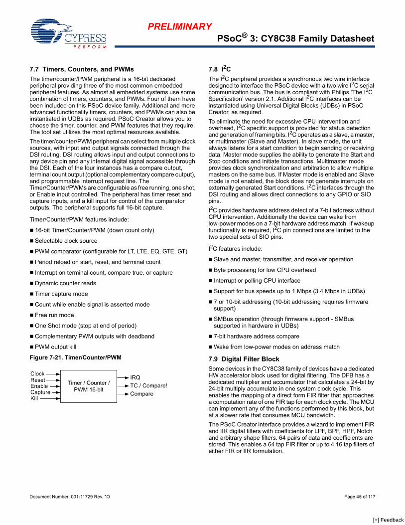
Full-speed (FS) USB 2.0 12 Mbps using internal oscillator[2]
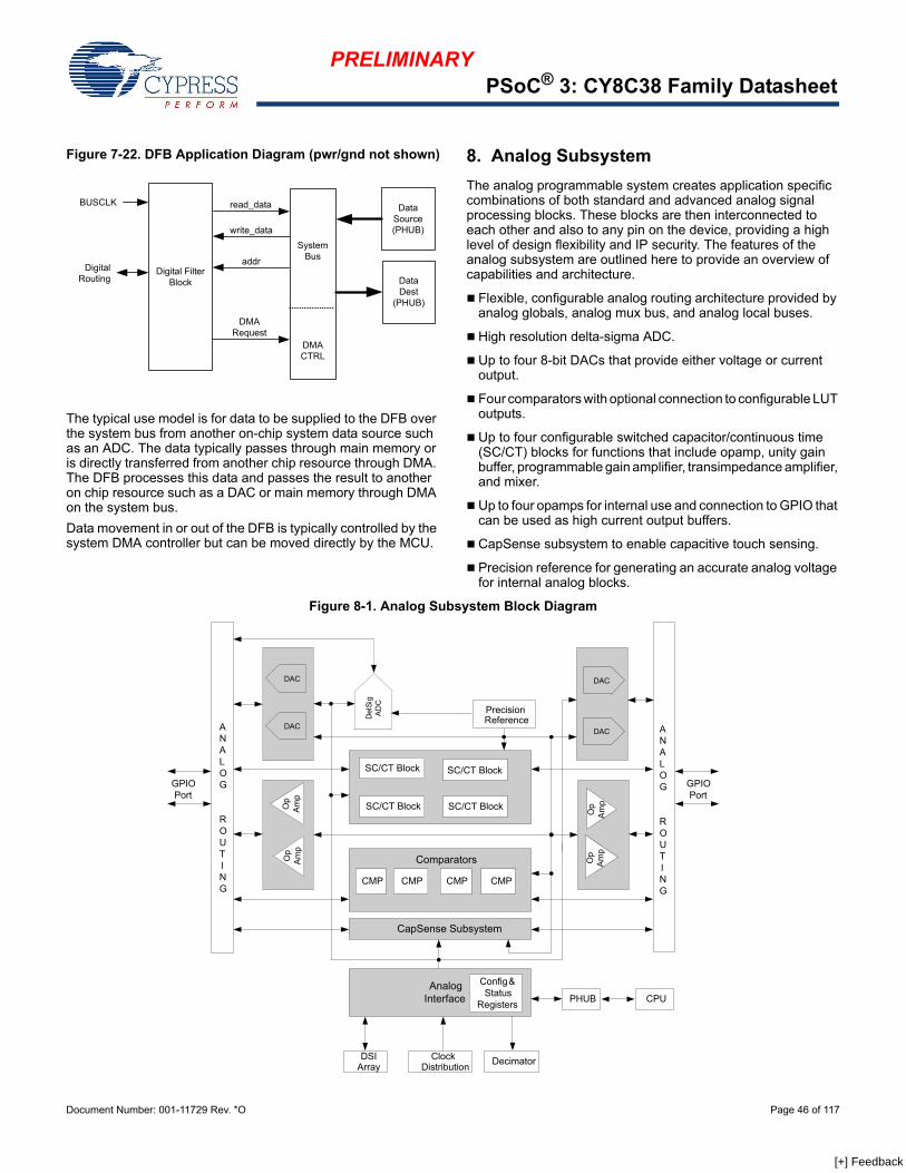
Up to four 16-bit configurable timer, counter, and PWM blocks Library of standard peripherals
• 8-, 16-, 24-, and 32-bit timers, counters, and PWMs
• Serial peripheral interface (SPI), universal asynchronous transmitter receiver (UART), and I2C
• Many others available in catalog Library of advanced peripherals
• Cyclic redundancy check (CRC)• Pseudo random sequence (PRS) generator• Local interconnect network (LIN) bus 2.0 • Quadrature decoder
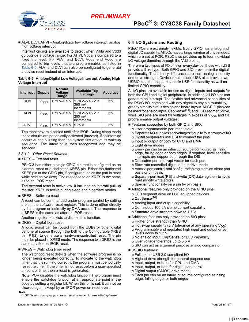
Analog peripherals (1.71 V VDDA 5.5 V) 1.024 V ± 0.1% internal voltage reference across –40 °C to
+85 °C (14 ppm/°C) Configurable delta-sigma ADC with 8- to 20-bit resolution
• Sample rates up to 192 ksps• Programmable gain stage: ×0.25 to ×16• 12-bit mode, 192 ksps, 70-dB signal-to-noise ratio (SNR),
67 MHz, 24-bit fixed point digital filter block (DFB) to implement FIR and IIR filters
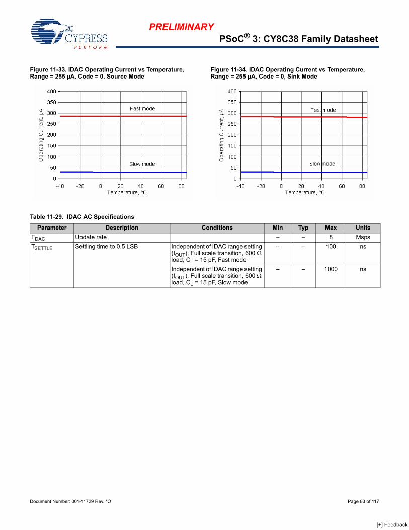
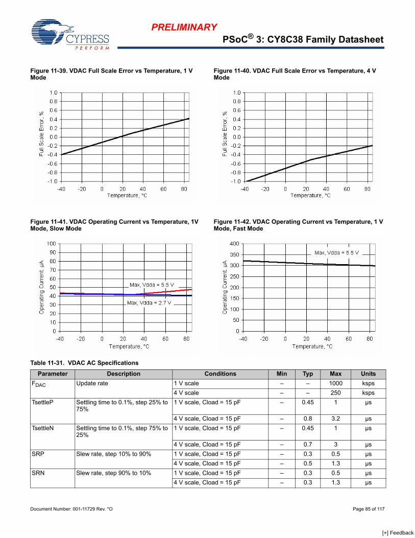
Up to four 8-bit, 8-Msps IDACs or 1-Msps VDACs Four comparators with 95-ns response time Up to four uncommitted opamps with 25-mA drive capability Up to four configurable multifunction analog blocks. Example
configurations are programmable gain amplifier (PGA), transimpedance amplifier (TIA), mixer, and sample and hold
CapSense support Programming, debug, and trace JTAG (4-wire), serial wire debug (SWD) (2-wire), and single
wire viewer (SWV) interfaces Eight address and one data breakpoint 4-KB instruction trace buffer Bootloader programming supportable through I2C, SPI,
UART, USB, and other interfaces Precision, programmable clocking 3- to 62-MHz internal oscillator over full temperature and
voltage range 4- to 33-MHz crystal oscillator for crystal PPM accuracy Internal PLL clock generation up to 67 MHz 32.768-kHz watch crystal oscillator Low-power internal oscillator at 1, 33, and 100 kHz
Temperature and packaging –40°C to +85 °C degrees industrial temperature 48-pin SSOP, 48-pin QFN, 68-pin QFN, and 100-pin TQFP
package options
Notes1. AHB – AMBA (advanced microcontroller bus architecture) high-performance bus, an ARM data transfer bus 2. This feature on select devices only. See Ordering Information on page 105 for details.3. GPIOs with opamp outputs are not recommended for use with CapSense.
4. CPU .......................................................................114.1 8051 CPU .....................................................114.2 Addressing Modes ........................................114.3 Instruction Set ...............................................114.4 DMA and PHUB ............................................154.5 Interrupt Controller ........................................17
6. System Integration ..............................................216.1 Clocking System ...........................................216.2 Power System ...............................................246.3 Reset .............................................................276.4 I/O System and Routing ................................28
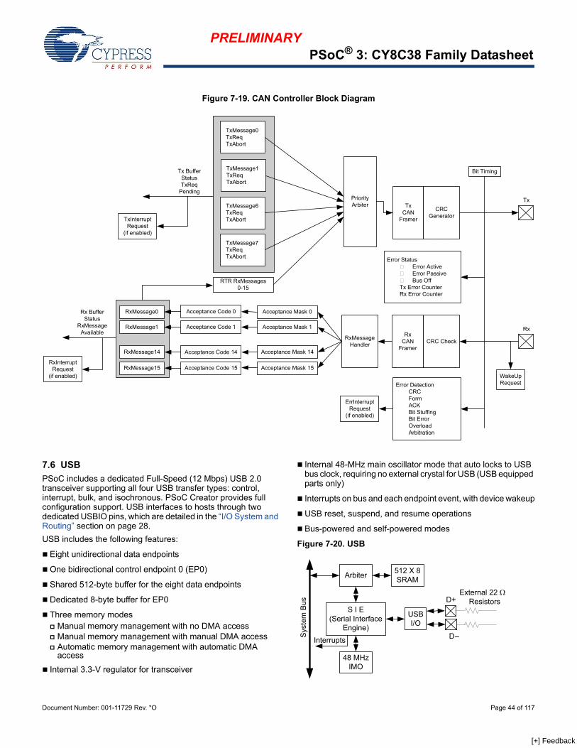
7. Digital Subsystem ...............................................347.1 Example Peripherals .....................................357.2 Universal Digital Block ..................................377.3 UDB Array Description ..................................417.4 DSI Routing Interface Description .................417.5 CAN ..............................................................437.6 USB ...............................................................447.7 Timers, Counters, and PWMs .......................457.8 I2C .................................................................457.9 Digital Filter Block .........................................45
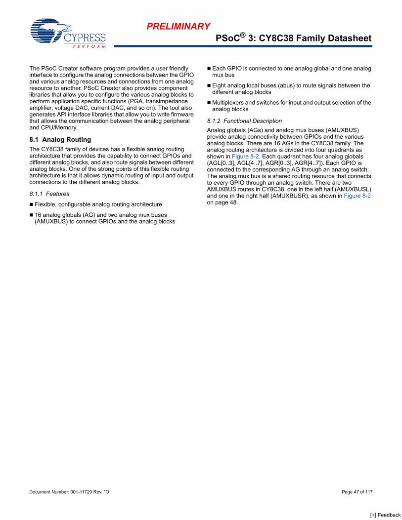
8. Analog Subsystem ..............................................468.1 Analog Routing .............................................478.2 Delta-sigma ADC ..........................................498.3 Comparators .................................................508.4 Opamps ........................................................518.5 Programmable SC/CT Blocks .......................528.6 LCD Direct Drive ...........................................53
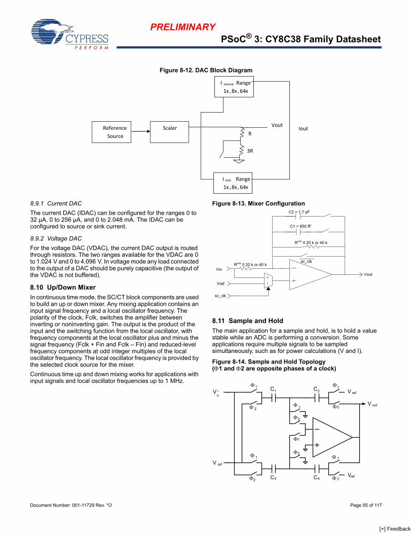
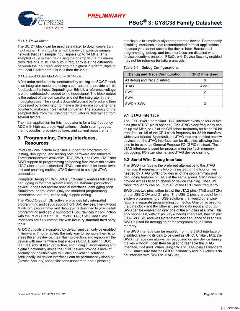
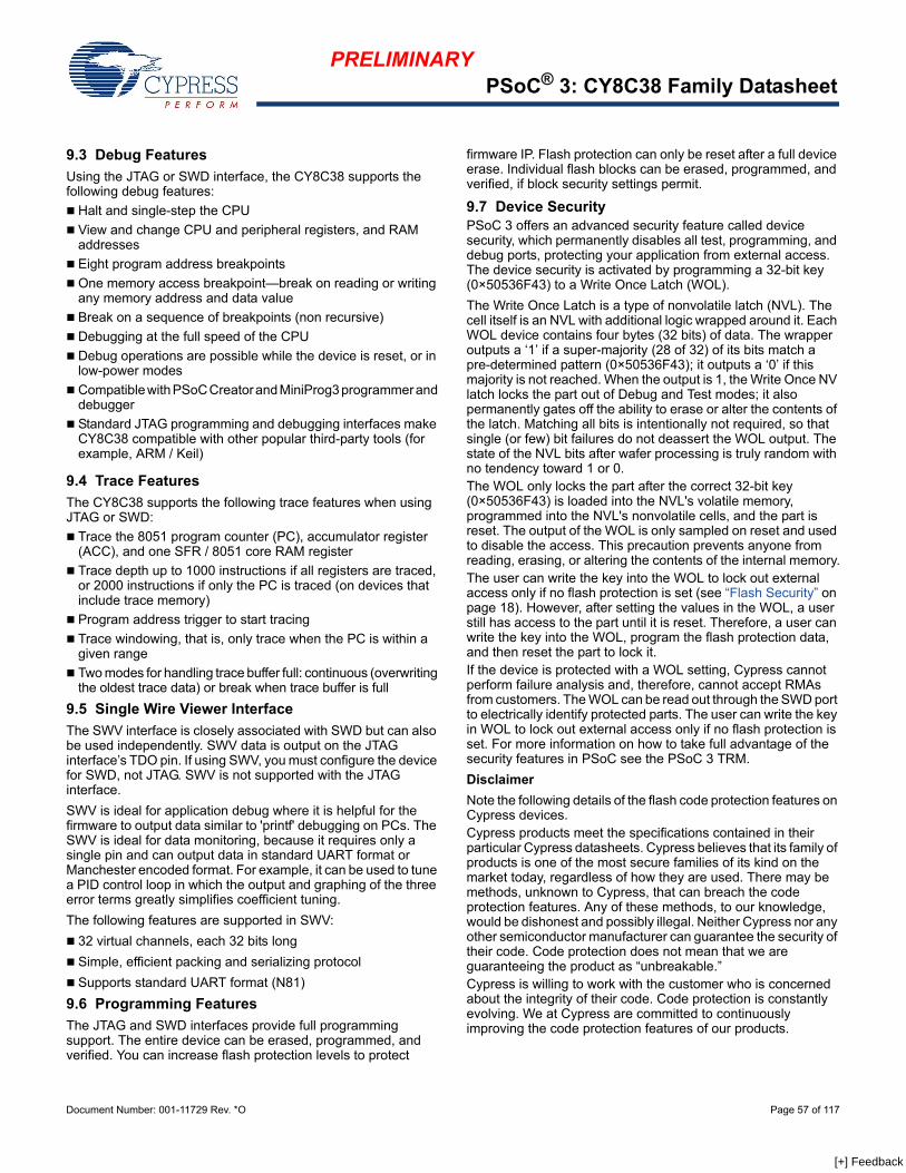
8.7 CapSense ..................................................... 548.8 Temp Sensor ................................................ 548.9 DAC .............................................................. 548.10 Up/Down Mixer ........................................... 558.11 Sample and Hold ........................................ 55
9. Programming, Debug Interfaces, Resources ... 569.1 JTAG Interface .............................................. 569.2 Serial Wire Debug Interface .......................... 569.3 Debug Features ............................................ 579.4 Trace Features ............................................. 579.5 Single Wire Viewer Interface ........................ 579.6 Programming Features ................................. 579.7 Device Security ............................................. 57
10. Development Support ....................................... 5810.1 Documentation ............................................ 5810.2 Online ......................................................... 5810.3 Tools ........................................................... 58
11. Electrical Specifications ................................... 5911.1 Absolute Maximum Ratings ........................ 5911.2 Device Level Specifications ........................ 6011.3 Power Regulators ....................................... 6311.4 Inputs and Outputs ..................................... 6511.5 Analog Peripherals ..................................... 6911.6 Digital Peripherals ....................................... 9111.7 Memory ....................................................... 9511.8 PSoC System Resources ......................... 10011.9 Clocking .................................................... 102
12. Ordering Information ...................................... 10512.1 Part Numbering Conventions .................... 107
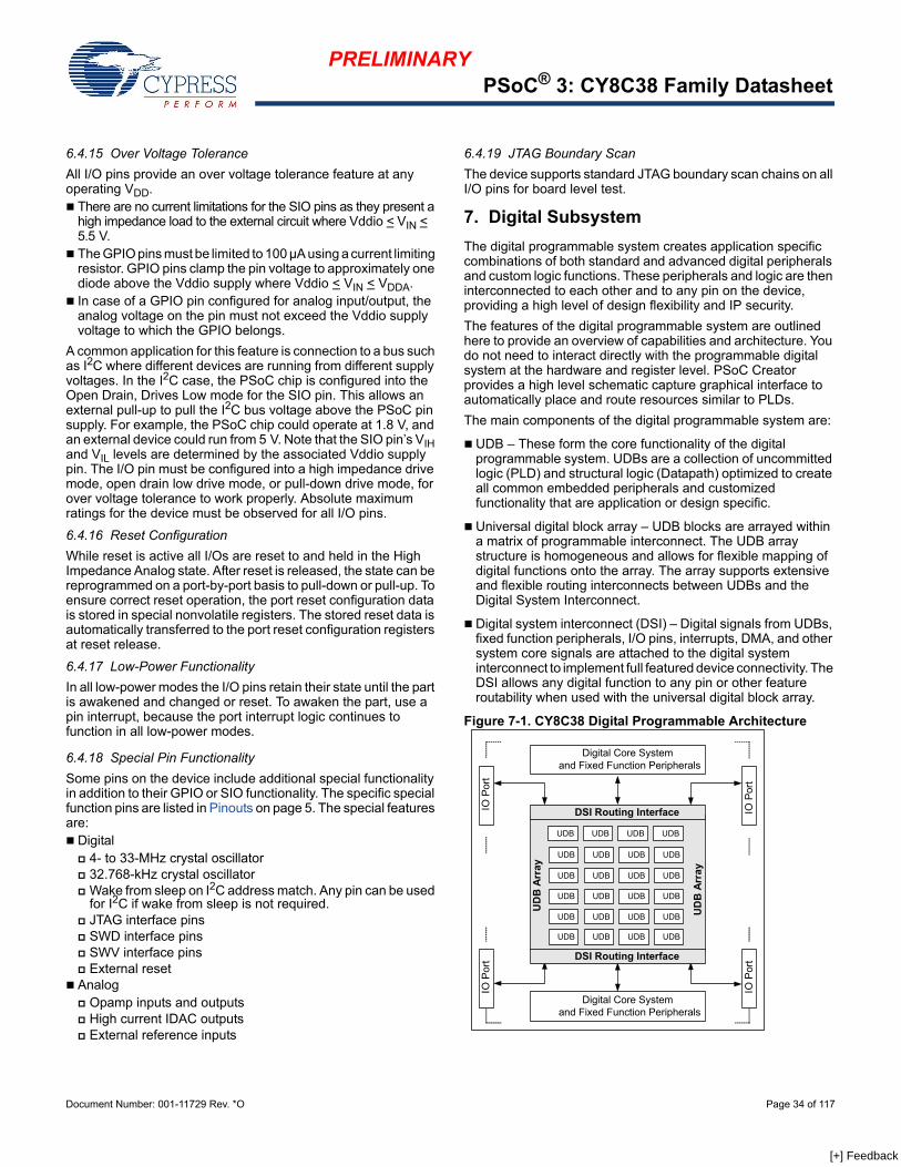
1. Architectural Overview Introducing the CY8C38 family of ultra low-power, flash Programmable System-on-Chip (PSoC®) devices, part of a scalable 8-bit PSoC 3 and 32-bit PSoC 5 platform. The CY8C38 family provides configurable blocks of analog, digital, and interconnect circuitry around a CPU subsystem. The combination of a CPU with a flexible analog subsystem, digital subsystem, routing, and I/O enables a high level of integration in a wide variety of consumer, industrial, and medical applications.
Figure 1-1. Simplified Block Diagram
Figure 1-1 illustrates the major components of the CY8C38 family. They are:
8051 CPU subsystem
Nonvolatile subsystem
Programming, debug, and test subsystem
Inputs and outputs
Clocking
Power
Digital subsystem
Analog subsystem
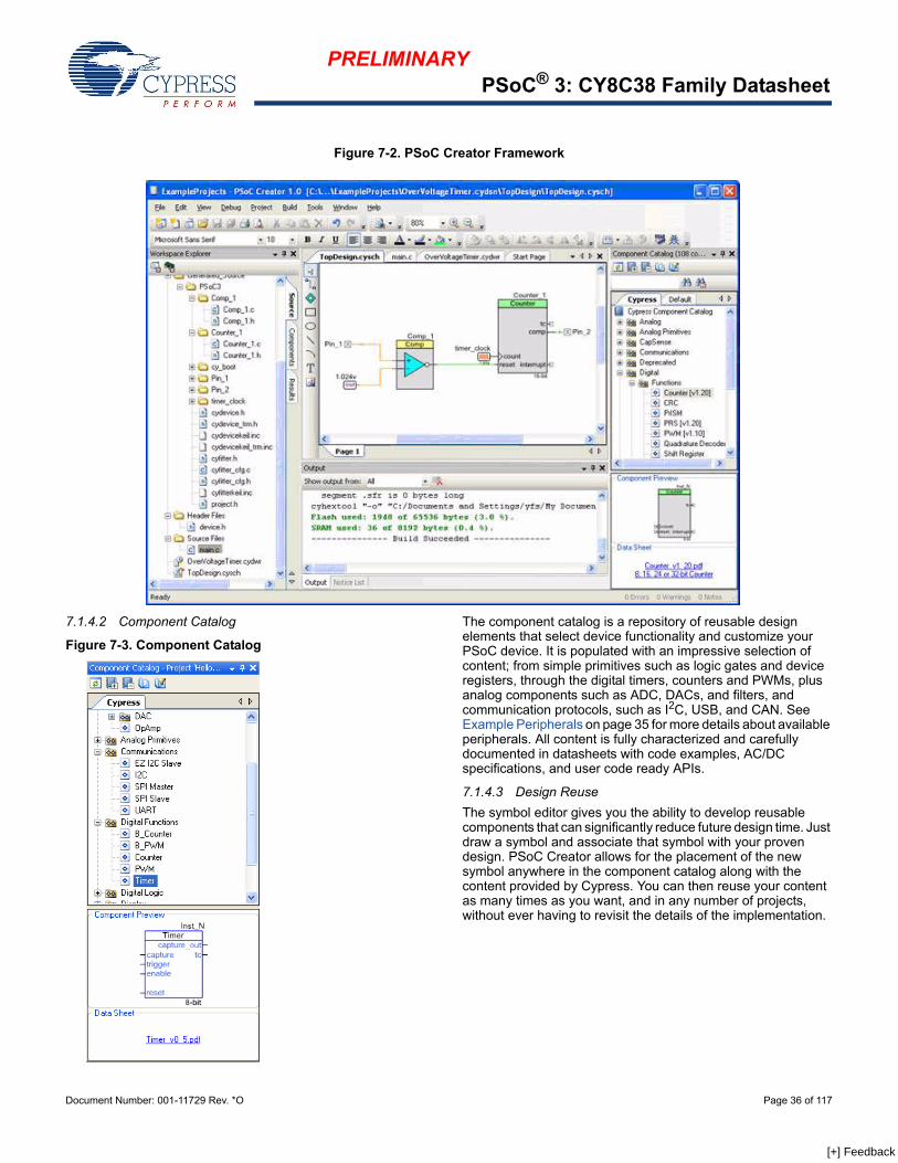
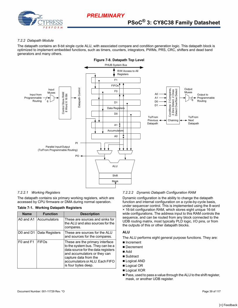
PSoC’s digital subsystem provides half of its unique configurability. It connects a digital signal from any peripheral to any pin through the digital system interconnect (DSI). It also provides functional flexibility through an array of small, fast, low-power UDBs. PSoC Creator provides a library of prebuilt and tested standard digital peripherals (UART, SPI, LIN, PRS, CRC, timer, counter, PWM, AND, OR, and so on) that are mapped to the UDB array. You can also easily create a digital circuit using boolean primitives by means of graphical design entry. Each UDB contains programmable array logic (PAL)/programmable logic device (PLD) functionality, together with a small state machine engine to support a wide variety of peripherals.
In addition to the flexibility of the UDB array, PSoC also provides configurable digital blocks targeted at specific functions. For the CY8C38 family these blocks can include four 16-bit timers, counters, and PWM blocks; I2C slave, master, and multimaster; FS USB; and Full CAN 2.0b.
For more details on the peripherals see the “Example Peripherals” section on page 35 of this datasheet. For information on UDBs, DSI, and other digital blocks, see the “Digital Subsystem” section on page 34 of this datasheet.
PSoC’s analog subsystem is the second half of its unique configurability. All analog performance is based on a highly accurate absolute voltage reference with less than 0.1-percent error over temperature and voltage. The configurable analog subsystem includes:
Analog muxes
Comparators
Voltage references
Analog-to-digital converter (ADC)
Digital-to-analog converters (DACs)
Digital filter block (DFB)
All GPIO pins can route analog signals into and out of the device using the internal analog bus. This allows the device to interface up to 62 discrete analog signals. The heart of the analog subsystem is a fast, accurate, configurable delta-sigma ADC with these features:
Less than 100 µV offset
A gain error of 0.2 percent
INL less than ±2 LSB
DNL less than ±1 LSB
SNR better than 89 dB in 16-bit mode
This converter addresses a wide variety of precision analog applications, including some of the most demanding sensors. The output of the ADC can optionally feed the programmable DFB through the DMA without CPU intervention. You can configure the DFB to perform IIR and FIR digital filters and several user-defined custom functions. The DFB can implement filters with up to 64 taps. It can perform a 48-bit multiply-accumulate (MAC) operation in one clock cycle.
Four high-speed voltage or current DACs support 8-bit output signals at an update rate of up to 8 Msps. They can be routed out of any GPIO pin. You can create higher resolution voltage PWM DAC outputs using the UDB array. This can be used to create a pulse width modulated (PWM) DAC of up to 10 bits, at up to 48 kHz. The digital DACs in each UDB support PWM, PRS, or delta-sigma algorithms with programmable widths. In addition to the ADC, DACs, and DFB, the analog subsystem provides multiple:
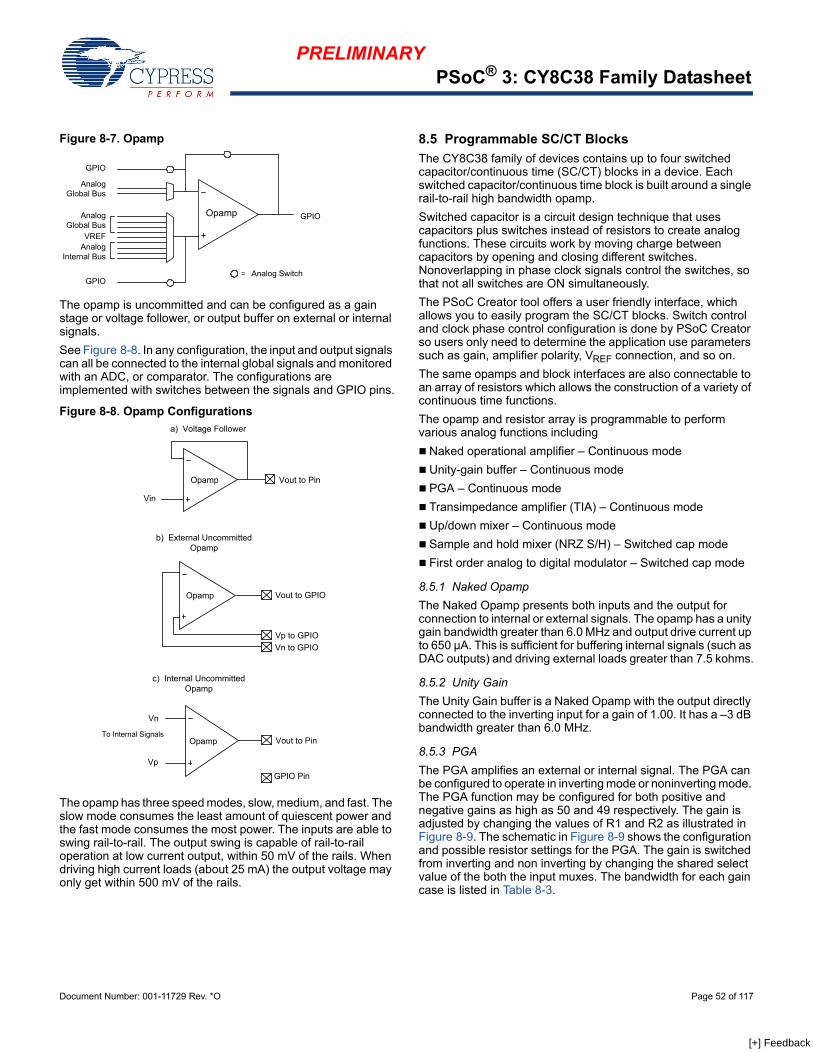
Uncommitted opamps
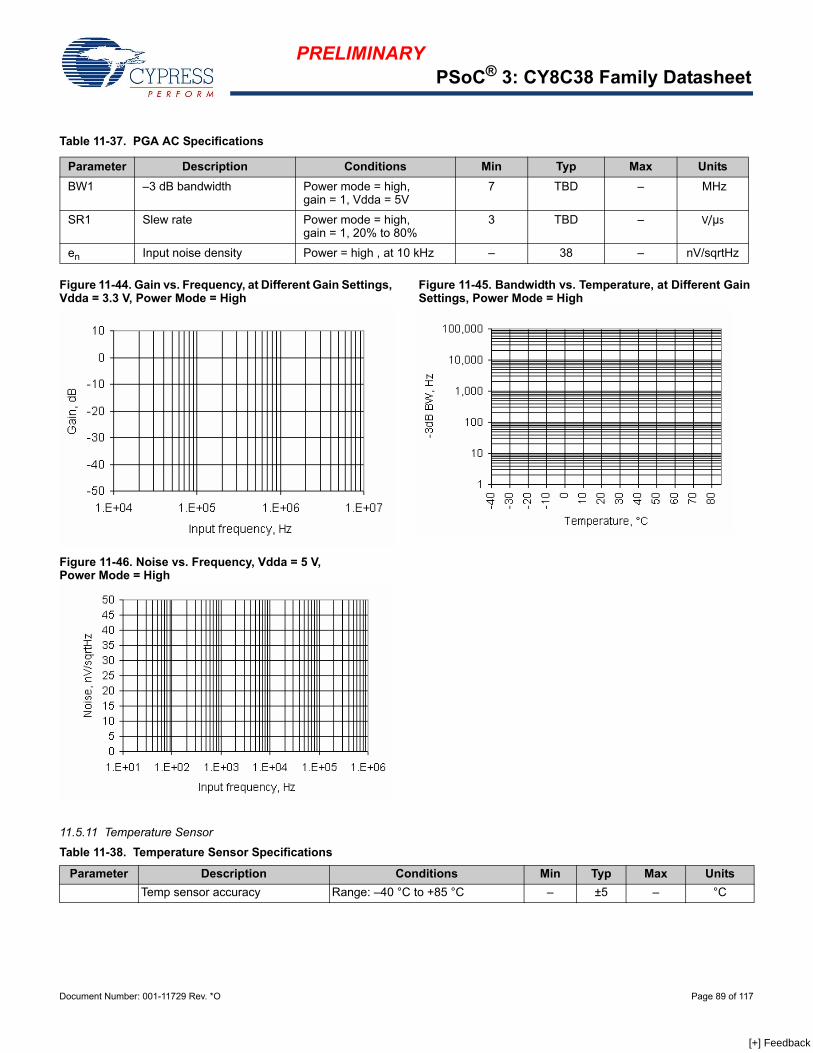
Configurable switched capacitor/continuous time (SC/CT) blocks. These support: Transimpedance amplifiers Programmable gain amplifiers Mixers Other similar analog components
See the “Analog Subsystem” section on page 46 of this datasheet for more details.
PSoC’s 8051 CPU subsystem is built around a single cycle pipelined 8051 8-bit processor running at up to 67 MHz. The CPU subsystem includes a programmable nested vector interrupt controller, DMA controller, and RAM. PSoC’s nested vector interrupt controller provides low latency by allowing the CPU to vector directly to the first address of the interrupt service routine, bypassing the jump instruction required by other architectures. The DMA controller enables peripherals to exchange data without CPU involvement. This allows the CPU to run slower (saving power) or use those CPU cycles to improve the performance of firmware algorithms. The single cycle 8051 CPU runs ten times faster than a standard 8051 processor. The processor speed itself is configurable, allowing you to tune active power consumption for specific applications.
PSoC’s nonvolatile subsystem consists of flash, byte-writeable EEPROM, and nonvolatile configuration options. It provides up to 64 KB of on-chip flash. The CPU can reprogram individual blocks of flash, enabling bootloaders. You can enable an error correcting code (ECC) for high reliability applications. A powerful and flexible protection model secures the user's sensitive information, allowing selective memory block locking for read and write protection. Up to 2 KB of byte-writeable EEPROM is available on-chip to store application data. Additionally, selected configuration options such as boot speed and pin drive mode are stored in nonvolatile memory. This allows settings to activate immediately after POR.
The three types of PSoC I/O are extremely flexible. All I/Os have many drive modes that are set at POR. PSoC also provides up to four I/O voltage domains through the Vddio pins. Every GPIO has analog I/O, LCD drive[4], CapSense[5], flexible interrupt generation, slew rate control, and digital I/O capability. The SIOs on PSoC allow VOH to be set independently of Vddio when used as outputs. When SIOs are in input mode they are high impedance. This is true even when the device is not powered or when the pin voltage goes above the supply voltage. This makes the SIO ideally suited for use on an I2C bus where the PSoC may not be powered when other devices on the bus are. The SIO pins also have high current sink capability for applications such as LED drives. The programmable input threshold feature of the SIO can be used to make the SIO function as a general purpose analog comparator. For devices with Full-Speed USB the USB physical interface is also provided (USBIO). When not using USB these pins may also be used for limited digital functionality and device programming. All of the features of the PSoC I/Os are covered in detail in the “I/O System and Routing” section on page 28 of this datasheet.
The PSoC device incorporates flexible internal clock generators, designed for high stability and factory trimmed for high accuracy. The internal main oscillator (IMO) is the master clock base for the system, and has 1-percent accuracy at 3 MHz. The IMO can be configured to run from 3 MHz up to 62 MHz. Multiple clock derivatives can be generated from the main clock frequency to meet application needs. The device provides a PLL to generate system clock frequencies up to 67 MHz from the IMO, external crystal, or external reference clock.
Notes4. This feature on select devices only. See Ordering Information on page 105 for details.5. GPIOs with opamp outputs are not recommended for use with CapSense.
It also contains a separate, very low-power internal low-speed oscillator (ILO) for the sleep and watchdog timers. A 32.768-kHz external watch crystal is also supported for use in real-time clock (RTC) applications. The clocks, together with programmable clock dividers, provide the flexibility to integrate most timing requirements.
The CY8C38 family supports a wide supply operating range from 1.71 V to 5.5 V. This allows operation from regulated supplies such as 1.8 V ± 5%, 2.5 V ±10%, 3.3 V ± 10%, or 5.0 V ± 10%, or directly from a wide range of battery types. In addition, it provides an integrated high efficiency synchronous boost converter that can power the device from supply voltages as low as 0.5 V. This enables the device to be powered directly from a single battery or solar cell. In addition, you can use the boost converter to generate other voltages required by the device, such as a 3.3-V supply for LCD glass drive. The boost’s output is available on the Vboost pin, allowing other devices in the application to be powered from the PSoC.
PSoC supports a wide range of low-power modes. These include a 200-nA hibernate mode with RAM retention and a 1-µA sleep mode with RTC. In the second mode, the optional 32.768-kHz watch crystal runs continuously and maintains an accurate RTC.
Power to all major functional blocks, including the programmable digital and analog peripherals, can be controlled independently by firmware. This allows low-power background processing when some peripherals are not in use. This, in turn, provides a total device current of only 1.2 mA when the CPU is running at 6 MHz, or 0.8 mA running at 3 MHz.
The details of the PSoC power modes are covered in the “Power System” section on page 24 of this datasheet.
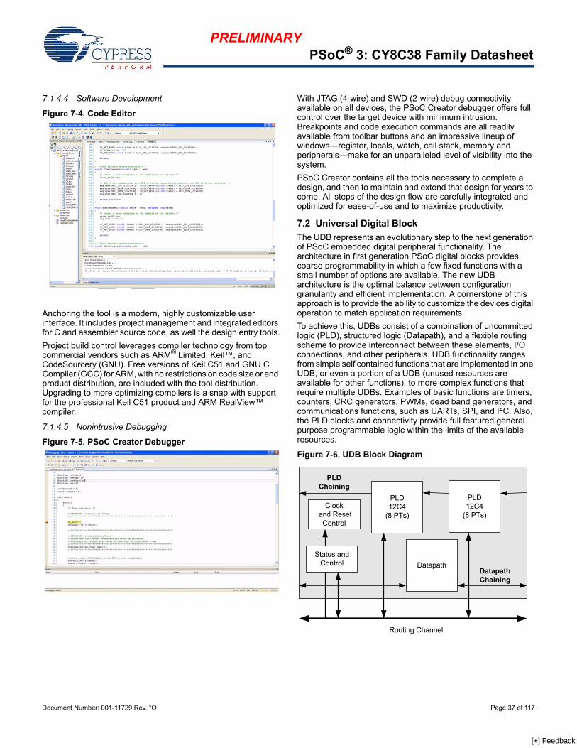
PSoC uses JTAG (4-wire) or SWD (2-wire) interfaces for programming, debug, and test. The 1-wire SWV may also be used for ‘printf’ style debugging. By combining SWD and SWV, you can implement a full debugging interface with just three pins. Using these standard interfaces you can debug or program the PSoC with a variety of hardware solutions from Cypress or third party vendors. PSoC supports on-chip break points and 4-KB instruction and data race memory for debug. Details of the programming, test, and debugging interfaces are discussed in the “Programming, Debug Interfaces, Resources” section on page 56 of this datasheet.
2. Pinouts
The Vddio pin that supplies a particular set of pins is indicated by the black lines drawn on the pinout diagrams in Figure 2-1 through Figure 2-4. Using the Vddio pins, a single PSoC can support multiple interface voltage levels, eliminating the need for off-chip level shifters. Each Vddio may sink up to 100 mA total to its associated I/O pins and opamps. On the 68-pin and 100-pin devices each set of Vddio associated pins may sink up to 100 mA. The 48-pin device may sink up to 100 mA total for all Vddio0 plus Vddio2 associated I/O pins and 100 mA total for all Vddio1 plus Vddio3 associated I/O pins.
Note6. Pins are No Connect (NC) on devices without USB. NC means that the pin has no electrical connection. The pin can be left floating or tied to a supply voltage or ground.
Notes7. Pins are No Connect (NC) on devices without USB. NC means that the pin has no electrical connection. The pin can be left floating or tied to a supply voltage or ground.8. The center pad on the QFN package should be connected to digital ground (VSSD) for best mechanical, thermal, and electrical performance. If not connected to ground,
it should be electrically floated and not connected to any other signal.
Notes9. The center pad on the QFN package should be connected to digital ground (VSSD) for best mechanical, thermal, and electrical performance. If not connected to
ground, it should be electrically floated and not connected to any other signal. 10. Pins are No Connect (NC) on devices without USB. NC means that the pin has no electrical connection. The pin can be left floating or tied to a supply voltage or ground.
Figure 2-5 and Figure 2-6 show an example schematic and an example PCB layout, for the 100-pin TQFP part, for optimal analog performance on a two-layer board.
The two pins labeled Vddd must be connected together.
The two pins labeled Vccd must be connected together, with capacitance added, as shown in Figure 2-5 and Power System on page 24. The trace between the two Vccd pins should be as short as possible.
The two pins labeled Vssd must be connected together.
Note11. Pins are No Connect (NC) on devices without USB. NC means that the pin has no electrical connection. The pin can be left floating or tied to a supply voltage or ground.
Figure 2-5. Example Schematic for 100-pin TQFP Part with Power Connections
Note The two Vccd pins must be connected together with as short a trace as possible. A trace under the device is recommended, asshown in Figure 2-6 on page 10.
Figure 2-6. Example PCB Layout for 100-pin TQFP Part for Optimal Analog Performance
3. Pin Descriptions
IDAC0, IDAC1, IDAC2, IDAC3
Low resistance output pin for high current DACs (IDAC).
OpAmp0out, OpAmp1out, OpAmp2out, OpAmp3out
High current output of uncommitted opamp[12].
Extref0, Extref1
External reference input to the analog system.
OpAmp0–, OpAmp1–, OpAmp2–, OpAmp3–
Inverting input to uncommitted opamp.
OpAmp0+, OpAmp1+, OpAmp2+, OpAmp3+
Noninverting input to uncommitted opamp.
GPIO
General purpose I/O pin provides interfaces to the CPU, digital peripherals, analog peripherals, interrupts, LCD segment drive, and CapSense[12].
I2C0: SCL, I2C1: SCL
I2C SCL line providing wake from sleep on an address match. Any I/O pin can be used for I2C SCL if wake from sleep is not required.
I2C0: SDA, I2C1: SDA
I2C SDA line providing wake from sleep on an address match. Any I/O pin can be used for I2C SDA if wake from sleep is not required.
Ind
Inductor connection to boost pump.
kHz XTAL: Xo, kHz XTAL: Xi
32.768-kHz crystal oscillator pin.
MHz XTAL: Xo, MHz XTAL: Xi
4- to 33-MHz crystal oscillator pin.
nTRST
Optional JTAG test reset programming and debug port connection to reset the JTAG connection.
SIO
Special I/O provides interfaces to the CPU, digital peripherals and interrupts with a programmable high threshold voltage, analog comparator, high sink current, and high impedance state when the device is unpowered.
SWDCK
Serial wire debug clock programming and debug port connection.
SWDIO
Serial wire debug input and output programming and debug port connection.
SWV.
Single wire viewer debug output.
TCK
JTAG test clock programming and debug port connection.
TDI
JTAG test data in programming and debug port connection.
TDO
JTAG test data out programming and debug port connection.
Vddd Vssd Vdda
Vssa
VssdPlane
VssaPlane
Note12. GPIOs with opamp outputs are not recommended for use with CapSense.
JTAG test mode select programming and debug port connection.
USBIO, D+
Provides D+ connection directly to a USB 2.0 bus. May be used as a digital I/O pin; it is powered from VDDD instead of from a Vddio. Pins are No Connect (NC) on devices without USB.[9]
USBIO, D–
Provides D– connection directly to a USB 2.0 bus. May be used as a digital I/O pin; it is powered from VDDD instead of from a Vddio. Pins are No Connect (NC) on devices without USB.[9]
Vboost
Power sense connection to boost pump.
Vbat
Battery supply to boost pump.
Vcca
Output of analog core regulator and input to analog core. Requires a 1-µF capacitor to VSSA. Regulator output not for external use.
Vccd
Output of digital core regulator and input to digital core. The two VCCD pins must be shorted together, with the trace between them as short as possible, and a 1-µF capacitor to VSSD; see Power System on page 24. Regulator output not for external use.
Vdda
Supply for all analog peripherals and analog core regulator. Vdda must be the highest voltage present on the device. All other supply pins must be less than or equal to Vdda.
Vddd
Supply for all digital peripherals and digital core regulator. Vddd must be less than or equal to Vdda.
Vssa
Ground for all analog peripherals.
Vssb
Ground connection for boost pump.
Vssd
Ground for all digital logic and I/O pins.
Vddio0, Vddio1, Vddio2, Vddio3
Supply for I/O pins. Each Vddio must be tied to a valid operating voltage (1.71 V to 5.5 V), and must be less than or equal to Vdda. If the I/O pins associated with Vddio0, Vddio2, or Vddio3 are not used then that Vddio should be tied to ground (Vssd or Vssa).
XRES (and configurable XRES)
External reset pin. Active low with internal pull-up. In 48-pin SSOP parts and 48-pin QFN parts, P1[2] may be configured as XRES. In all other parts the pin is configured as a GPIO.
4. CPU
4.1 8051 CPU
The CY8C38 devices use a single cycle 8051 CPU, which is fully compatible with the original MCS-51 instruction set. The CY8C38 family uses a pipelined RISC architecture, which executes most instructions in 1 to 2 cycles to provide peak performance of up to 33 MIPS with an average of 2 cycles per instruction. The single cycle 8051 CPU runs ten times faster than a standard 8051 processor.
The 8051 CPU subsystem includes these features:
Single cycle 8051 CPU
Up to 64 KB of flash memory, up to 2 KB of EEPROM, and up to 8 KB of SRAM
Programmable nested vector interrupt controller
DMA controller
Peripheral HUB (PHUB)
External memory interface (EMIF)
4.2 Addressing Modes
The following addressing modes are supported by the 8051:
Direct Addressing: The operand is specified by a direct 8-bit address field. Only the internal RAM and the SFRs can be accessed using this mode.
Indirect Addressing: The instruction specifies the register which contains the address of the operand. The registers R0 or R1 are used to specify the 8-bit address, while the data pointer (DPTR) register is used to specify the 16-bit address.
Register Addressing: Certain instructions access one of the registers (R0 to R7) in the specified register bank. These instructions are more efficient because there is no need for an address field.
Register Specific Instructions: Some instructions are specific to certain registers. For example, some instructions always act on the accumulator. In this case, there is no need to specify the operand.
Immediate Constants: Some instructions carry the value of the constants directly instead of an address.
Indexed Addressing: This type of addressing can be used only for a read of the program memory. This mode uses the Data Pointer as the base and the accumulator value as an offset to read a program memory.
Bit Addressing: In this mode, the operand is one of 256 bits.
4.3 Instruction Set
The 8051 instruction set is highly optimized for 8-bit handling and Boolean operations. The types of instructions supported include:
Arithmetic instructions support the direct, indirect, register, immediate constant, and register-specific instructions. Arithmetic modes are used for addition, subtraction, multiplication, division, increment, and decrement operations. Table 4-1 lists the different arithmetic instructions.
4.3.1.2 Logical Instructions
The logical instructions perform Boolean operations such as AND, OR, XOR on bytes, rotate of accumulator contents, and swap of nibbles in an accumulator. The Boolean operations on the bytes are performed on the bit-by-bit basis. Table 4-2 shows the list of logical instructions and their description.
Table 4-1. Arithmetic Instructions
Mnemonic Description Bytes Cycles
ADD A,Rn Add register to accumulator 1 1
ADD A,Direct Add direct byte to accumulator 2 2
ADD A,@Ri Add indirect RAM to accumulator 1 2
ADD A,#data Add immediate data to accumulator 2 2
ADDC A,Rn Add register to accumulator with carry 1 1
ADDC A,Direct Add direct byte to accumulator with carry 2 2
ADDC A,@Ri Add indirect RAM to accumulator with carry 1 2
ADDC A,#data Add immediate data to accumulator with carry 2 2
SUBB A,Rn Subtract register from accumulator with borrow 1 1
SUBB A,Direct Subtract direct byte from accumulator with borrow 2 2
SUBB A,@Ri Subtract indirect RAM from accumulator with borrow 1 2
SUBB A,#data Subtract immediate data from accumulator with borrow 2 2
The data transfer instructions are of three types: the core RAM, xdata RAM, and the lookup tables. The core RAM transfer includes transfer between any two core RAM locations or SFRs. These instructions can use direct, indirect, register, and immediate addressing. The xdata RAM transfer includes only the transfer between the accumulator and the xdata RAM location. It can use only indirect addressing. The lookup tables involve nothing but the read of program memory using the Indexed
addressing mode. Table 4-3 lists the various data transfer instructions available.
4.3.1.4 Boolean Instructions
The 8051 core has a separate bit-addressable memory location. It has 128 bits of bit addressable RAM and a set of SFRs that are bit addressable. The instruction set includes the whole menu of bit operations such as move, set, clear, toggle, OR, and AND instructions and the conditional jump instructions. Table 4-4 lists the available Boolean instructions.
ANL Direct, #data AND immediate data to direct byte 3 3
ORL A,Rn OR register to accumulator 1 1
ORL A,Direct OR direct byte to accumulator 2 2
ORL A,@Ri OR indirect RAM to accumulator 1 2
ORL A,#data OR immediate data to accumulator 2 2
ORL Direct, A OR accumulator to direct byte 2 3
ORL Direct, #data OR immediate data to direct byte 3 3
XRL A,Rn XOR register to accumulator 1 1
XRL A,Direct XOR direct byte to accumulator 2 2
XRL A,@Ri XOR indirect RAM to accumulator 1 2
XRL A,#data XOR immediate data to accumulator 2 2
XRL Direct, A XOR accumulator to direct byte 2 3
XRL Direct, #data XOR immediate data to direct byte 3 3
CLR A Clear accumulator 1 1
CPL A Complement accumulator 1 1
RL A Rotate accumulator left 1 1
RLC A Rotate accumulator left through carry 1 1
RR A Rotate accumulator right 1 1
RRC A Rotate accumulator right though carry 1 1
SWAP A Swap nibbles within accumulator 1 1
Table 4-2. Logical Instructions (continued)
Mnemonic Description Bytes Cycles
Table 4-3. Data Transfer Instructions
Mnemonic Description Bytes Cycles
MOV A,Rn Move register to accumulator 1 1
MOV A,Direct Move direct byte to accumulator 2 2
MOV A,@Ri Move indirect RAM to accumulator 1 2
MOV A,#data Move immediate data to accumulator 2 2
The 8051 supports a set of conditional and unconditional jump instructions that help to modify the program execution flow. Table 4-5 shows the list of jump instructions.
4.4 DMA and PHUB
The PHUB and the DMA controller are responsible for data transfer between the CPU and peripherals, and also data transfers between peripherals. The PHUB and DMA also control device configuration during boot. The PHUB consists of:
A central hub that includes the DMA controller, arbiter, and router
Multiple spokes that radiate outward from the hub to most peripherals
There are two PHUB masters: the CPU and the DMA controller. Both masters may initiate transactions on the bus. The DMA channels can handle peripheral communication without CPU intervention. The arbiter in the central hub determines which DMA channel is the highest priority if there are multiple requests.
4.4.1 PHUB Features
CPU and DMA controller are both bus masters to the PHUB
Eight multi-layer AHB bus parallel access paths (spokes) for peripheral access
Simultaneous CPU and DMA access to peripherals located on different spokes
Simultaneous DMA source and destination burst transactions on different spokes
Supports 8-, 16-, 24-, and 32-bit addressing and data
Table 4-5. Jump Instructions
Mnemonic Description Bytes Cycles
ACALL addr11 Absolute subroutine call 2 4
LCALL addr16 Long subroutine call 3 4
RET Return from subroutine 1 4
RETI Return from interrupt 1 4
AJMP addr11 Absolute jump 2 3
LJMP addr16 Long jump 3 4
SJMP rel Short jump (relative address) 2 3
JMP @A + DPTR Jump indirect relative to DPTR 1 5
JZ rel Jump if accumulator is zero 2 4
JNZ rel Jump if accumulator is nonzero 2 4
CJNE A,Direct, rel Compare direct byte to accumulator and jump if not equal 3 5
CJNE A, #data, rel Compare immediate data to accumulator and jump if not equal 3 4
CJNE Rn, #data, rel Compare immediate data to register and jump if not equal 3 4
CJNE @Ri, #data, rel Compare immediate data to indirect RAM and jump if not equal 3 5
DJNZ Rn,rel Decrement register and jump if not zero 2 4
DJNZ Direct, rel Decrement direct byte and jump if not zero 3 5
NOP No operation 1 1
Table 4-6. PHUB Spokes and Peripherals
PHUB Spokes Peripherals
0 SRAM
1 IOs, PICU, EMIF
2 PHUB local configuration, Power manager, Clocks, IC, SWV, EEPROM, Flash programming interface
Each channel has one or more transaction descriptors (TD) to configure channel behavior. Up to 128 total TDs can be defined
TDs can be dynamically updated
Eight levels of priority per channel
Any digitally routable signal, the CPU, or another DMA channel, can trigger a transaction
Each channel can generate up to two interrupts per transfer
Transactions can be stalled or canceled
Supports transaction size of infinite or 1 to 64 KB
TDs may be nested and/or chained for complex transactions
4.4.3 Priority Levels
The CPU always has higher priority than the DMA controller when their accesses require the same bus resources. Due to the system architecture, the CPU can never starve the DMA. DMA channels of higher priority (lower priority number) may interrupt current DMA transfers. In the case of an interrupt, the current transfer is allowed to complete its current transaction. To ensure latency limits when multiple DMA accesses are requested simultaneously, a fairness algorithm guarantees an interleaved minimum percentage of bus bandwidth for priority levels 2 through 7. Priority levels 0 and 1 do not take part in the fairness algorithm and may use 100 percent of the bus bandwidth. If a tie occurs on two DMA requests of the same priority level, a simple round robin method is used to evenly share the allocated bandwidth. The round robin allocation can be disabled for each DMA channel, allowing it to always be at the head of the line. Priority levels 2 to 7 are guaranteed the minimum bus bandwidth shown in Table 4-7 after the CPU and DMA priority levels 0 and 1 have satisfied their requirements.
When the fairness algorithm is disabled, DMA access is granted based solely on the priority level; no bus bandwidth guarantees are made.
4.4.4 Transaction Modes Supported
The flexible configuration of each DMA channel and the ability to chain multiple channels allow the creation of both simple and complex use cases. General use cases include, but are not limited to:
4.4.4.1 Simple DMA
In a simple DMA case, a single TD transfers data between a source and sink (peripherals or memory location).
4.4.4.2 Auto Repeat DMA
Auto repeat DMA is typically used when a static pattern is repetitively read from system memory and written to a peripheral. This is done with a single TD that chains to itself.
4.4.4.3 Ping Pong DMA
A ping pong DMA case uses double buffering to allow one buffer to be filled by one client while another client is consuming the data previously received in the other buffer. In its simplest form, this is done by chaining two TDs together so that each TD calls the opposite TD when complete.
4.4.4.4 Circular DMA
Circular DMA is similar to ping pong DMA except it contains more than two buffers. In this case there are multiple TDs; after the last TD is complete it chains back to the first TD.
4.4.4.5 Scatter Gather DMA
In the case of scatter gather DMA, there are multiple noncontiguous sources or destinations that are required to effectively carry out an overall DMA transaction. For example, a packet may need to be transmitted off of the device and the packet elements, including the header, payload, and trailer, exist in various noncontiguous locations in memory. Scatter gather DMA allows the segments to be concatenated together by using multiple TDs in a chain. The chain gathers the data from the multiple locations. A similar concept applies for the reception of data onto the device. Certain parts of the received data may need to be scattered to various locations in memory for software processing convenience. Each TD in the chain specifies the location for each discrete element in the chain.
4.4.4.6 Packet Queuing DMA
Packet queuing DMA is similar to scatter gather DMA but specifically refers to packet protocols. With these protocols, there may be separate configuration, data, and status phases associated with sending or receiving a packet.
For instance, to transmit a packet, a memory mapped configuration register can be written inside a peripheral, specifying the overall length of the ensuing data phase. The CPU can set up this configuration information anywhere in system memory and copy it with a simple TD to the peripheral. After the configuration phase, a data phase TD (or a series of data phase TDs) can begin (potentially using scatter gather). When the data phase TD(s) finish, a status phase TD can be invoked that reads some memory mapped status information from the peripheral and copies it to a location in system memory specified by the CPU for later inspection. Multiple sets of configuration, data, and status phase ‘subchains’ can be strung together to create larger chains that transmit multiple packets in this way. A similar concept exists in the opposite direction to receive the packets.
One TD may modify another TD, as the TD configuration spaceis memory mapped similar to any other peripheral. For example,a first TD loads a second TD’s configuration and then calls thesecond TD. The second TD moves data as required by theapplication. When complete, the second TD calls the first TD,which again updates the second TD’s configuration. Thisprocess repeats as often as necessary.
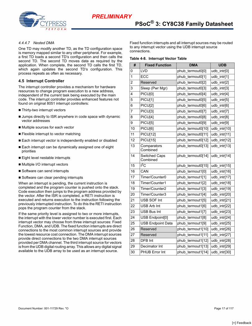
4.5 Interrupt Controller
The interrupt controller provides a mechanism for hardware resources to change program execution to a new address, independent of the current task being executed by the main code. The interrupt controller provides enhanced features not found on original 8051 interrupt controllers:
Thirty-two interrupt vectors
Jumps directly to ISR anywhere in code space with dynamic vector addresses
Multiple sources for each vector
Flexible interrupt to vector matching
Each interrupt vector is independently enabled or disabled
Each interrupt can be dynamically assigned one of eight priorities
Eight level nestable interrupts
Multiple I/O interrupt vectors
Software can send interrupts
Software can clear pending interrupts
When an interrupt is pending, the current instruction is completed and the program counter is pushed onto the stack. Code execution then jumps to the program address provided by the vector. After the ISR is completed, a RETI instruction is executed and returns execution to the instruction following the previously interrupted instruction. To do this the RETI instruction pops the program counter from the stack.
If the same priority level is assigned to two or more interrupts, the interrupt with the lower vector number is executed first. Each interrupt vector may choose from three interrupt sources: Fixed Function, DMA, and UDB. The fixed function interrupts are direct connections to the most common interrupt sources and provide the lowest resource cost connection. The DMA interrupt sources provide direct connections to the two DMA interrupt sources provided per DMA channel. The third interrupt source for vectors is from the UDB digital routing array. This allows any digital signal available to the UDB array to be used as an interrupt source.
Fixed function interrupts and all interrupt sources may be routed to any interrupt vector using the UDB interrupt source connections.
Table 4-8. Interrupt Vector Table
# Fixed Function DMA UDB
0 LVD phub_termout0[0] udb_intr[0]
1 ECC phub_termout0[1] udb_intr[1]
2 Reserved phub_termout0[2] udb_intr[2]
3 Sleep (Pwr Mgr) phub_termout0[3] udb_intr[3]
4 PICU[0] phub_termout0[4] udb_intr[4]
5 PICU[1] phub_termout0[5] udb_intr[5]
6 PICU[2] phub_termout0[6] udb_intr[6]
7 PICU[3] phub_termout0[7] udb_intr[7]
8 PICU[4] phub_termout0[8] udb_intr[8]
9 PICU[5] phub_termout0[9] udb_intr[9]
10 PICU[6] phub_termout0[10] udb_intr[10]
11 PICU[12] phub_termout0[11] udb_intr[11]
12 PICU[15] phub_termout0[12] udb_intr[12]
13 Comparators Combined
phub_termout0[13] udb_intr[13]
14 Switched Caps Combined
phub_termout0[14] udb_intr[14]
15 I2C phub_termout0[15] udb_intr[15]
16 CAN phub_termout1[0] udb_intr[16]
17 Timer/Counter0 phub_termout1[1] udb_intr[17]
18 Timer/Counter1 phub_termout1[2] udb_intr[18]
19 Timer/Counter2 phub_termout1[3] udb_intr[19]
20 Timer/Counter3 phub_termout1[4] udb_intr[20]
21 USB SOF Int phub_termout1[5] udb_intr[21]
22 USB Arb Int phub_termout1[6] udb_intr[22]
23 USB Bus Int phub_termout1[7] udb_intr[23]
24 USB Endpoint[0] phub_termout1[8] udb_intr[24]
25 USB Endpoint Data phub_termout1[9] udb_intr[25]
CY8C38 SRAM is used for temporary data storage. Up to 8 KB of SRAM is provided and can be accessed by the 8051 or the DMA controller. See Memory Map on page 19. Simultaneous access of SRAM by the 8051 and the DMA controller is possible if different 4-KB blocks are accessed.
5.2 Flash Program Memory
Flash memory in PSoC devices provides nonvolatile storage for user firmware, user configuration data, bulk data storage, and optional ECC data. The main flash memory area contains up to 64 KB of user program space.
Up to an additional 8 KB of flash space is available for ECC. If ECC is not used this space can store device configuration data and bulk user data. User code may not be run out of the ECC flash memory section. ECC can correct one bit error and detect two bit errors per 8 bytes of firmware memory; an interrupt can be generated when an error is detected.
Flash is read in units of rows; each row is 9 bytes wide with 8 bytes of data and 1 byte of ECC data. When a row is read, the data bytes are copied into an 8-byte instruction buffer. The CPU fetches its instructions from this buffer, for improved CPU performance.
Flash programming is performed through a special interface and preempts code execution out of flash. The flash programming interface performs flash erasing, programming and setting code protection levels. Flash in-system serial programming (ISSP), typically used for production programming, is possible through both the SWD and JTAG interfaces. In-system programming, typically used for bootloaders, is also possible using serial interfaces such as I2C, USB, UART, and SPI, or any communications protocol.
5.3 Flash Security
All PSoC devices include a flexible flash-protection model that prevents access and visibility to on-chip flash memory. This prevents duplication or reverse engineering of proprietary code. Flash memory is organized in blocks, where each block contains 256 bytes of program or data and 32 bytes of ECC or configuration data. A total of up to 256 blocks is provided on 64-KB flash devices.
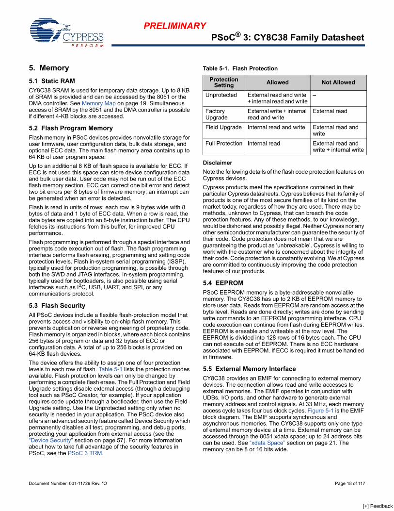
The device offers the ability to assign one of four protection levels to each row of flash. Table 5-1 lists the protection modes available. Flash protection levels can only be changed by performing a complete flash erase. The Full Protection and Field Upgrade settings disable external access (through a debugging tool such as PSoC Creator, for example). If your application requires code update through a bootloader, then use the Field Upgrade setting. Use the Unprotected setting only when no security is needed in your application. The PSoC device also offers an advanced security feature called Device Security which permanently disables all test, programming, and debug ports, protecting your application from external access (see the “Device Security” section on page 57). For more information about how to take full advantage of the security features in PSoC, see the PSoC 3 TRM.
Disclaimer
Note the following details of the flash code protection features on Cypress devices.
Cypress products meet the specifications contained in their particular Cypress datasheets. Cypress believes that its family of products is one of the most secure families of its kind on the market today, regardless of how they are used. There may be methods, unknown to Cypress, that can breach the code protection features. Any of these methods, to our knowledge, would be dishonest and possibly illegal. Neither Cypress nor any other semiconductor manufacturer can guarantee the security of their code. Code protection does not mean that we are guaranteeing the product as ‘unbreakable’. Cypress is willing to work with the customer who is concerned about the integrity of their code. Code protection is constantly evolving. We at Cypress are committed to continuously improving the code protection features of our products.
5.4 EEPROM
PSoC EEPROM memory is a byte-addressable nonvolatile memory. The CY8C38 has up to 2 KB of EEPROM memory to store user data. Reads from EEPROM are random access at the byte level. Reads are done directly; writes are done by sending write commands to an EEPROM programming interface. CPU code execution can continue from flash during EEPROM writes. EEPROM is erasable and writeable at the row level. The EEPROM is divided into 128 rows of 16 bytes each. The CPU can not execute out of EEPROM. There is no ECC hardware associated with EEPROM. If ECC is required it must be handled in firmware.
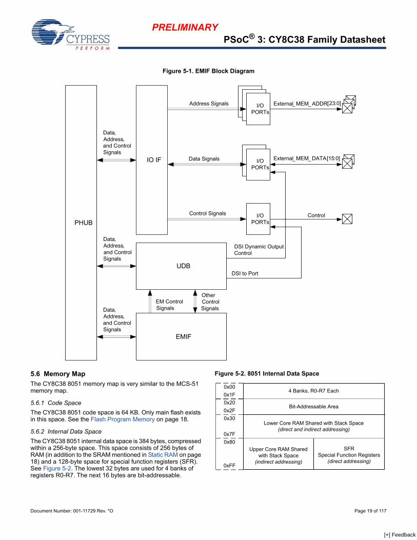
5.5 External Memory Interface
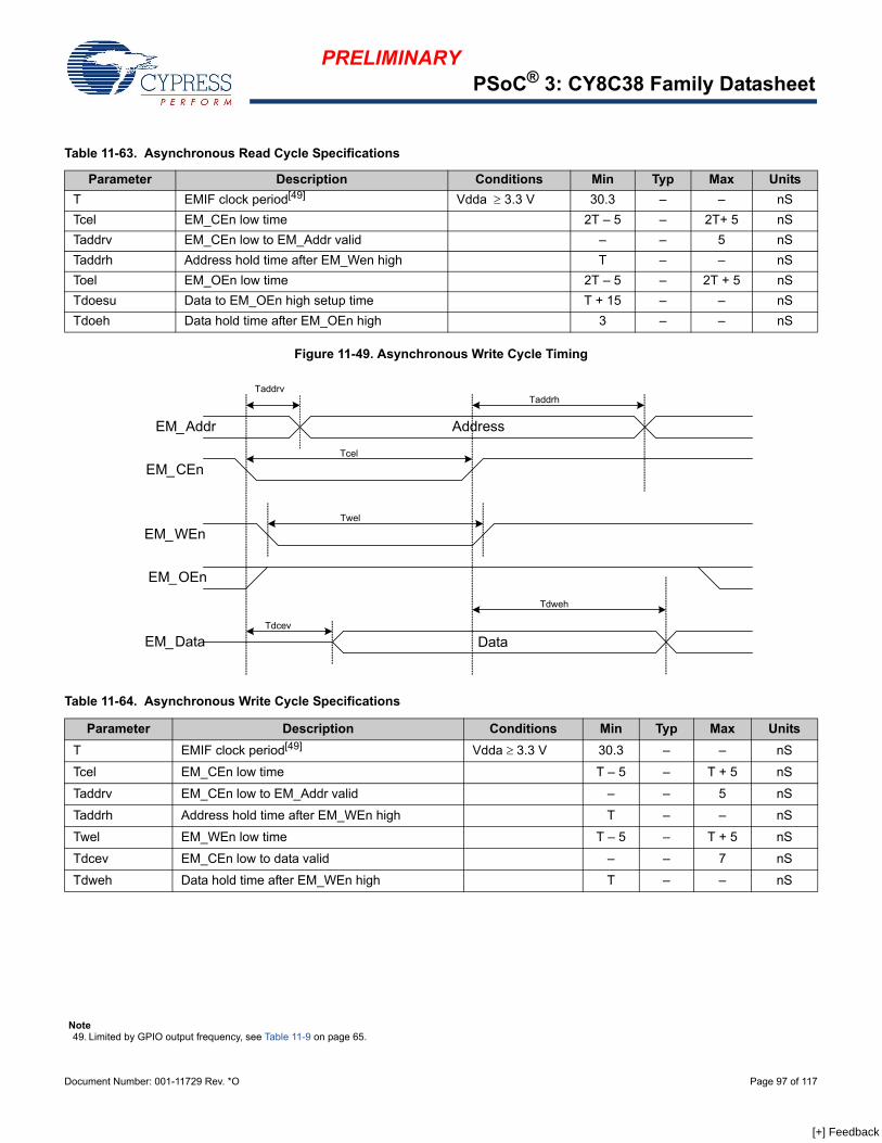
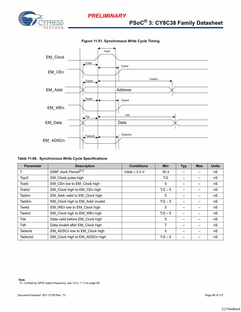
CY8C38 provides an EMIF for connecting to external memory devices. The connection allows read and write accesses to external memories. The EMIF operates in conjunction with UDBs, I/O ports, and other hardware to generate external memory address and control signals. At 33 MHz, each memory access cycle takes four bus clock cycles. Figure 5-1 is the EMIF block diagram. The EMIF supports synchronous and asynchronous memories. The CY8C38 supports only one type of external memory device at a time. External memory can be accessed through the 8051 xdata space; up to 24 address bits can be used. See “xdata Space” section on page 21. The memory can be 8 or 16 bits wide.
Table 5-1. Flash Protection
ProtectionSetting Allowed Not Allowed
Unprotected External read and write + internal read and write
–
Factory Upgrade
External write + internal read and write
External read
Field Upgrade Internal read and write External read and write
Full Protection Internal read External read and write + internal write
The CY8C38 8051 memory map is very similar to the MCS-51 memory map.
5.6.1 Code Space
The CY8C38 8051 code space is 64 KB. Only main flash exists in this space. See the Flash Program Memory on page 18.
5.6.2 Internal Data Space
The CY8C38 8051 internal data space is 384 bytes, compressed within a 256-byte space. This space consists of 256 bytes of RAM (in addition to the SRAM mentioned in Static RAM on page 18) and a 128-byte space for special function registers (SFR). See Figure 5-2. The lowest 32 bytes are used for 4 banks of registers R0-R7. The next 16 bytes are bit-addressable.
Figure 5-2. 8051 Internal Data Space
PHUB
IO IF
UDB
EMIF
I/O PORTs
I/O PORTs
I/O PORTs
Data, Address, and Control Signals
Data, Address, and Control Signals
Address Signals
Data Signals
Control Signals
Data, Address, and Control Signals
EM Control Signals
Other Control Signals
DSI Dynamic Output Control
DSI to Port
Control
External_MEM_ DATA[15:0]
External_MEM_ ADDR[23:0]
Upper Core RAM Shared with Stack Space
(indirect addressing)
SFRSpecial Function Registers
(direct addressing)
Lower Core RAM Shared with Stack Space(direct and indirect addressing)
In addition to the register or bit address modes used with the lower 48 bytes, the lower 128 bytes can be accessed with direct or indirect addressing. With direct addressing mode, the upper 128 bytes map to the SFRs. With indirect addressing mode, the upper 128 bytes map to RAM. Stack operations use indirect addressing; the 8051 stack space is 256 bytes. See the “Addressing Modes” section on page 11.
5.6.3 SFRs
The SFR space provides access to frequently accessed registers. The memory map for the SFR memory space is shown in Table 5-2.
The CY8C38 family provides the standard set of registers found on industry standard 8051 devices. In addition, the CY8C38 devices add SFRs to provide direct access to the I/O ports on the device. The following sections describe the SFRs added to the CY8C38 family.
XData Space Access SFRs
The 8051 core features dual DPTR registers for faster data transfer operations. The data pointer select SFR, DPS, selects which data pointer register, DPTR0 or DPTR1, is used for the following instructions:
MOVX @DPTR, A
MOVX A, @DPTR
MOVC A, @A+DPTR
JMP @A+DPTR
INC DPTR
MOV DPTR, #data16
The extended data pointer SFRs, DPX0, DPX1, MXAX, and P2AX, hold the most significant parts of memory addresses during access to the xdata space. These SFRs are used only with the MOVX instructions.
During a MOVX instruction using the DPTR0/DPTR1 register, the most significant byte of the address is always equal to the contents of DPX0/DPX1.
During a MOVX instruction using the R0 or R1 register, the most significant byte of the address is always equal to the contents of MXAX, and the next most significant byte is always equal to the contents of P2AX.
I/O Port SFRs
The I/O ports provide digital input sensing, output drive, pin interrupts, connectivity for analog inputs and outputs, LCD, and access to peripherals through the DSI. Full information on I/O ports is found in I/O System and Routing on page 28.
I/O ports are linked to the CPU through the PHUB and are also available in the SFRs. Using the SFRs allows faster access to a limited set of I/O port registers, while using the PHUB allows boot configuration and access to all I/O port registers.
Each SFR supported I/O port provides three SFRs:
SFRPRTxDR sets the output data state of the port (where × is port number and includes ports 0–6, 12 and 15).
The SFRPRTxSEL selects whether the PHUB PRTxDR register or the SFRPRTxDR controls each pin’s output buffer within the port. If a SFRPRTxSEL[y] bit is high, the corresponding SFRPRTxDR[y] bit sets the output state for that pin. If a SFRPRTxSEL[y] bit is low, the corresponding PRTxDR[y] bit sets the output state of the pin (where y varies from 0 to 7).
The SFRPRTxPS is a read only register that contains pin state values of the port pins.
The 8051 xdata space is 24-bit, or 16 MB in size. The majority of this space is not ‘external’—it is used by on-chip components. See Table 5-3. External, that is, off-chip, memory can be accessed using the EMIF. See External Memory Interface on page 18.
6. System Integration
6.1 Clocking System
The clocking system generates, divides, and distributes clocks throughout the PSoC system. For the majority of systems, no external crystal is required. The IMO and PLL together can generate up to a 66 MHz clock, accurate to ±1 percent over voltage and temperature. Additional internal and external clock sources allow each design to optimize accuracy, power, and cost. All of the system clock sources can be used to generate other clock frequencies in the 16-bit clock dividers and UDBs for anything the user wants, for example a UART baud rate generator.
Clock generation and distribution is automatically configured through the PSoC Creator IDE graphical interface. This is based on the complete system’s requirements. It greatly speeds the design process. PSoC Creator allows you to build clocking systems with minimal input. You can specify desired clock frequencies and accuracies, and the software locates or builds a clock that meets the required specifications. This is possible because of the programmability inherent PSoC.
Key features of the clocking system include:
Seven general purpose clock sources 3- to 62-MHz IMO, ±1% at 3 MHz 4- to 33-MHz external crystal oscillator (MHzECO) Clock doubler provides a doubled clock frequency output for
the USB block, see USB Clock Domain on page 23. DSI signal from an external I/O pin or other logic 24- to 67-MHz fractional PLL sourced from IMO, MHzECO,
or DSI Clock doubler 1-kHz, 33-kHz, 100-kHz ILO for WDT and sleep timer 32.768-kHz external crystal oscillator (kHzECO) for RTC
IMO has a USB mode that auto locks to the USB bus clock requiring no external crystal for USB. (USB equipped parts only)
Independently sourced clock in all clock dividers
Eight 16-bit clock dividers for the digital system
Four 16-bit clock dividers for the analog system
Dedicated 16-bit divider for the bus clock
Dedicated 4-bit divider for the CPU clock
Automatic clock configuration in PSoC Creator
Table 5-3. XDATA Data Address Map
Address Range Purpose
0×00 0000 – 0×00 1FFF SRAM
0×00 4000 – 0×00 42FF Clocking, PLLs, and oscillators
0×00 4300 – 0×00 43FF Power management
0×00 4400 – 0×00 44FF Interrupt controller
0×00 4500 – 0×00 45FF Ports interrupt control
0×00 4700 – 0×00 47FF Flash programming interface
0×00 4900 – 0×00 49FF I2C controller
0×00 4E00 – 0×00 4EFF Decimator
0×00 4F00 – 0×00 4FFF Fixed timer/counter/PWMs
0×00 5000 – 0×00 51FF I/O ports control
0×00 5400 – 0×00 54FF EMIF control registers
0×00 5800 – 0×00 5FFF Analog subsystem interface
0×00 6000 – 0×00 60FF USB controller
0×00 6400 – 0×00 6FFF UDB configuration
0×00 7000 – 0×00 7FFF PHUB configuration
0×00 8000 – 0×00 8FFF EEPROM
0×00 A000 – 0×00 A400 CAN
0×00 C000 – 0×00 C800 DFB
0×01 0000 – 0×01 FFFF Digital Interconnect configuration
0×05 0220 – 0×05 02F0 Debug controller
0×08 0000 – 0×08 1FFF Flash ECC bytes
0×80 0000 – 0×FF FFFF External memory interface
Table 6-1. Oscillator Summary
Source Fmin Tolerance at Fmin Fmax Tolerance at Fmax Startup Time
IMO 3 MHz ±1% over voltage and temperature 62 MHz ±7% 10 µs max
MHzECO 4 MHz Crystal dependent 33 MHz Crystal dependent 5 ms typ, max is crystal dependent
In most designs the IMO is the only clock source required, due to its ±1-percent accuracy. The IMO operates with no external components and outputs a stable clock. A factory trim for each frequency range is stored in the device. With the factory trim, tolerance varies from ±1 percent at 3 MHz, up to ±7 percent at 62 MHz. The IMO, in conjunction with the PLL, allows generation of CPU and system clocks up to the device's maximum frequency (see PLL). The IMO provides clock outputs at 3, 6, 12, 24, 48, and 62 MHz.
6.1.1.2 Clock Doubler
The clock doubler outputs a clock at twice the frequency of the input clock. The doubler works for input frequency ranges of 6 to 24 MHz (providing 12 to 48 MHz at the output). It can be configured to use a clock from the IMO, MHzECO, or the DSI (external pin). The doubler is typically used to clock the USB.
6.1.1.3 PLL
The PLL allows low-frequency, high-accuracy clocks to be multiplied to higher frequencies. This is a trade off between higher clock frequency and accuracy and, higher power consumption and increased startup time.
The PLL block provides a mechanism for generating clock frequencies based upon a variety of input sources. The PLL outputs clock frequencies in the range of 24 to 67 MHz. Its input and feedback dividers supply 4032 discrete ratios to create almost any desired system clock frequency. The accuracy of the PLL output depends on the accuracy of the PLL input source. The most common PLL use is to multiply the IMO clock at 3 MHz, where it is most accurate, to generate the CPU and system clocks up to the device’s maximum frequency.
The PLL achieves phase lock within 250 µs (verified by bit setting). It can be configured to use a clock from the IMO, MHzECO or DSI (external pin). The PLL clock source can be used until lock is complete and signaled with a lock bit. The lock signal can be routed through the DSI to generate an interrupt. Disable the PLL before entering low-power modes.
6.1.1.4 Internal Low-Speed Oscillator
The ILO provides clock frequencies for low-power consumption, including the watchdog timer, and sleep timer. The ILO generates up to three different clocks: 1 kHz, 33 kHz, and 100 kHz. The 1-kHz clock (CLK1K) is typically used for a background ‘heartbeat’ timer. This clock inherently lends itself to low-power supervisory operations such as the watchdog timer and long sleep intervals using the central timewheel (CTW).
The central timewheel is a 1-kHz, free running, 13-bit counter clocked by the ILO. The central timewheel is always enabled, except in hibernate mode and when the CPU is stopped during debug on chip mode. It can be used to generate periodic interrupts for timing purposes or to wake the system from a low-power mode. Firmware can reset the central timewheel. Systems that require accurate timing should use the RTC capability instead of the central timewheel.
The 100-kHz clock (CLK100K) works as a low-power system clock to run the CPU. It can also generate time intervals such as fast sleep intervals using the fast timewheel. The fast timewheel is a 100-kHz, 5-bit counter clocked by the ILO that can also be used to wake the system. The fast timewheel settings are programmable, and the counter automatically resets when the terminal count is reached. This enables flexible, periodic wakeups of the CPU at a higher rate than is allowed using the central timewheel. The fast timewheel can generate an optional interrupt each time the terminal count is reached.
The 33-kHz clock (CLK33K) comes from a divide-by-3 operation on CLK100K. This output can be used as a reduced accuracy version of the 32.768-kHz ECO clock with no need for a crystal.
6.1.2 External Oscillators
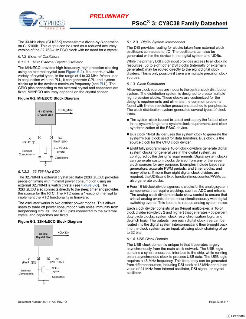
6.1.2.1 MHz External Crystal Oscillator
The MHzECO provides high frequency, high precision clocking using an external crystal (see Figure 6-2). It supports a wide variety of crystal types, in the range of 4 to 33 MHz. When used in conjunction with the PLL, it can generate CPU and system clocks up to the device's maximum frequency (see PLL). The GPIO pins connecting to the external crystal and capacitors are fixed. MHzECO accuracy depends on the crystal chosen.
Figure 6-2. MHzECO Block Diagram
6.1.2.2 32.768-kHz ECO
The 32.768-kHz external crystal oscillator (32kHzECO) provides precision timing with minimal power consumption using an external 32.768-kHz watch crystal (see Figure 6-3). The 32kHzECO also connects directly to the sleep timer and provides the source for the RTC. The RTC uses a 1-second interrupt to implement the RTC functionality in firmware.
The oscillator works in two distinct power modes. This allows users to trade off power consumption with noise immunity from neighboring circuits. The GPIO pins connected to the external crystal and capacitors are fixed.
Figure 6-3. 32kHzECO Block Diagram
6.1.2.3 Digital System Interconnect
The DSI provides routing for clocks taken from external clock oscillators connected to I/O. The oscillators can also be generated within the device in the digital system and UDBs.
While the primary DSI clock input provides access to all clocking resources, up to eight other DSI clocks (internally or externally generated) may be routed directly to the eight digital clock dividers. This is only possible if there are multiple precision clock sources.
6.1.3 Clock Distribution
All seven clock sources are inputs to the central clock distribution system. The distribution system is designed to create multiple high precision clocks. These clocks are customized for the design’s requirements and eliminate the common problems found with limited resolution prescalers attached to peripherals. The clock distribution system generates several types of clock trees.
The system clock is used to select and supply the fastest clock in the system for general system clock requirements and clock synchronization of the PSoC device.
Bus clock 16-bit divider uses the system clock to generate the system's bus clock used for data transfers. Bus clock is the source clock for the CPU clock divider.
Eight fully programmable 16-bit clock dividers generate digital system clocks for general use in the digital system, as configured by the design’s requirements. Digital system clocks can generate custom clocks derived from any of the seven clock sources for any purpose. Examples include baud rate generators, accurate PWM periods, and timer clocks, and many others. If more than eight digital clock dividers are required, the UDBs and fixed function timer/counter/PWMs can also generate clocks.
Four 16-bit clock dividers generate clocks for the analog system components that require clocking, such as ADC and mixers. The analog clock dividers include skew control to ensure that critical analog events do not occur simultaneously with digital switching events. This is done to reduce analog system noise.
Each clock divider consists of an 8-input multiplexer, a 16-bit clock divider (divide by 2 and higher) that generates ~50 percent duty cycle clocks, system clock resynchronization logic, and deglitch logic. The outputs from each digital clock tree can be routed into the digital system interconnect and then brought back into the clock system as an input, allowing clock chaining of up to 32 bits.
6.1.4 USB Clock Domain
The USB clock domain is unique in that it operates largely asynchronously from the main clock network. The USB logic contains a synchronous bus interface to the chip, while running on an asynchronous clock to process USB data. The USB logic requires a 48 MHz frequency. This frequency can be generated from different sources, including DSI clock at 48 MHz or doubled value of 24 MHz from internal oscillator, DSI signal, or crystal oscillator.
The power system consists of separate analog, digital, and I/O supply pins, labeled Vdda, Vddd, and Vddiox, respectively. It also includes two internal 1.8-V regulators that provide the digital (Vccd) and analog (Vcca) supplies for the internal core logic. The output pins of the regulators (Vccd and Vcca) and the Vddio pins must have capacitors connected as shown in Figure 6-4. The two Vccd pins must be shorted together, with as short a trace as possible, and connected to a 1-µF ±10-percent X5R capacitor. The power system also contains a sleep regulator, an I2C regulator, and a hibernate regulator.
Figure 6-4. PSoC Power System
Note The two Vccd pins must be connected together with as short a trace as possible. A trace under the device is recommended, asshown in Figure 2-6 on page 10.
PSoC 3 devices have four different power modes, as shown in Table 6-2 and Table 6-3. The power modes allow a design to easily provide required functionality and processing power while simultaneously minimizing power consumption and maximizing battery life in low-power and portable devices.
PSoC 3 power modes, in order of decreasing power consumption are:
Active
Alternate Active
Sleep
Hibernate
Active is the main processing mode. Its functionality is configurable. Each power controllable subsystem is enabled or disabled by using separate power configuration template registers. In alternate active mode, fewer subsystems are enabled, reducing power. In sleep mode most resources are disabled regardless of the template settings. Sleep mode is optimized to provide timed sleep intervals and Real Time Clock functionality. The lowest power mode is hibernate, which retains register and SRAM state, but no clocks, and allows wakeup only from I/O pins. Figure 6-5 on page 26 illustrates the allowable transitions between power modes
Table 6-2. Power Modes
Power Modes Description Entry Condition Wakeup Source Active Clocks Regulator
Active Primary mode of operation, all peripherals available (programmable)
Wakeup, reset, manual register entry
Any interrupt Any (programmable)
All regulators available. Digital and analog regulators can be disabled if external regulation used.
Alternate Active
Similar to Active mode, and is typically configured to have fewer peripherals active to reduce power. One possible configuration is to turn off the CPU and flash, and run peripherals at full speed
Manual register entry
Any interrupt Any (programmable)
All regulators available. Digital and analog regulators can be disabled if external regulation used.
Sleep All subsystems automatically disabled
Manual register entry
Comparator, PICU, I2C, RTC, CTW, LVD
ILO/kHzECO Both digital and analog regulators buzzed. Digital and analog regulators can be disabled if external regulation used.
Hibernate All subsystems automatically disabled Lowest power consuming mode with all peripherals and internal regulators disabled, except hibernate regulator is enabledConfiguration and memory contents retained
Manual register entry
PICU Only hibernate regulator active.
Table 6-3. Power Modes Wakeup Time and Power Consumption
Sleep Modes
Wakeup Time
Current (typ)
Code Execution
Digital Resources
Analog Resources
Clock Sources Available Wakeup Sources Reset
Sources
Active – 1.2 mA[13] Yes All All All – All
Alternate Active
– TBD User defined
All All All – All
Sleep<15 µs 1 µA No I2C Comparator ILO/kHzECO Comparator,
PICU, I2C, RTC, CTW, LVD
XRES, LVD, WDR
Hibernate <100 µs 200 nA No None None None PICU XRES
Active mode is the primary operating mode of the device. When in active mode, the active configuration template bits control which available resources are enabled or disabled. When a resource is disabled, the digital clocks are gated, analog bias currents are disabled, and leakage currents are reduced as appropriate. User firmware can dynamically control subsystem power by setting and clearing bits in the active configuration template. The CPU can disable itself, in which case the CPU is automatically reenabled at the next wakeup event.
When a wakeup event occurs, the global mode is always returned to active, and the CPU is automatically enabled, regardless of its template settings. Active mode is the default global power mode upon boot.
6.2.1.2 Alternate Active Mode
Alternate Active mode is very similar to Active mode. In alternate active mode, fewer subsystems are enabled, to reduce power consumption. One possible configuration is to turn off the CPU and flash, and run peripherals at full speed.
6.2.1.3 Sleep Mode
Sleep mode reduces power consumption when a resume time of 15 µs is acceptable. The wake time is used to ensure that the regulator outputs are stable enough to directly enter active mode.
6.2.1.4 Hibernate Mode
In hibernate mode nearly all of the internal functions are disabled. Internal voltages are reduced to the minimal level to keep vital systems alive. Configuration state is preserved in hibernate mode and SRAM memory is retained. GPIOs configured as digital outputs maintain their previous values and external GPIO pin interrupt settings are preserved. The device can only return from hibernate mode in response to an external I/O interrupt. The resume time from hibernate mode is less than 100 µs.
6.2.1.5 Wakeup Events
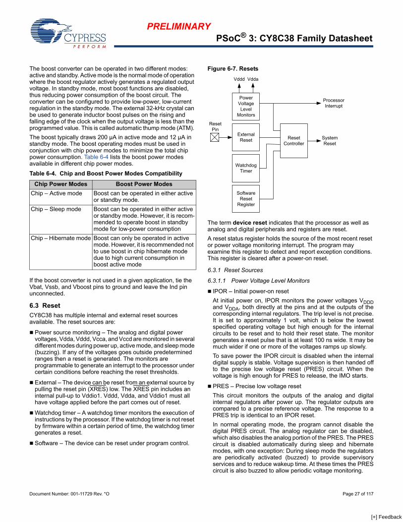
Wakeup events are configurable and can come from an interrupt or device reset. A wakeup event restores the system to active mode. Firmware enabled interrupt sources include internally generated interrupts, power supervisor, central timewheel, and I/O interrupts. Internal interrupt sources can come from a variety
of peripherals, such as analog comparators and UDBs. The central timewheel provides periodic interrupts to allow the system to wake up, poll peripherals, or perform real-time functions. Reset event sources include the external reset I/O pin (XRES), WDT, and precision reset (PRES).
6.2.2 Boost Converter
Applications that use a supply voltage of less than 1.71 V, such as solar or single cell battery supplies, may use the on-chip boost converter. The boost converter may also be used in any system that requires a higher operating voltage than the supply provides. For instance, this includes driving 5.0 V LCD glass in a 3.3 V system. The boost converter accepts an input voltage as low as 0.5 V. With one low cost inductor it produces a selectable output voltage sourcing enough current to operate the PSoC and other on-board components.
The boost converter accepts an input voltage from 0.5 V to 5.5 V (VBAT), and can start up with Vbat as low as 0.5 V. The converter provides a user configurable output voltage of 1.8 to 5.0 V (Vboost). Vbat is typically less than Vboost; if Vbat is greater than or equal to Vboost, then Vboost will be the same as Vbat. The block can deliver up to 50 mA (IBOOST) depending on configuration.
Four pins are associated with the boost converter: Vbat, Vssb, Vboost, and Ind. The boosted output voltage is sensed at the Vboost pin and must be connected directly to the chip’s supply inputs. An inductor is connected between the Vbat and Ind pins. You can optimize the inductor value to increase the boost converter efficiency based on input voltage, output voltage, current and switching frequency. The External Schottky diode shown in Figure 6-6 is required only in cases when Vboost > 3.6 V.
Figure 6-6. Application for Boost Converter
The switching frequency can be set to 100 kHz, 400 kHz, 2 MHz, or 32 kHz to optimize efficiency and component cost. The 100 kHz, 400 kHz, and 2 MHz switching frequencies are generated using oscillators internal to the boost converter block. When the 32-kHz switching frequency is selected, the clock is derived from a 32 kHz external crystal oscillator. The 32-kHz external clock is primarily intended for boost standby mode.
At 2 MHz the Vboost output is limited to 2 × Vbat, and at 400 kHz Vboost is limited to 4 × Vbat.
Active
Manual
Hibernate
Alternate Active
Sleep
Buzz
Note13. IMO 6 MHz, CPU 6 MHz, all peripherals disabled
The boost converter can be operated in two different modes: active and standby. Active mode is the normal mode of operation where the boost regulator actively generates a regulated output voltage. In standby mode, most boost functions are disabled, thus reducing power consumption of the boost circuit. The converter can be configured to provide low-power, low-current regulation in the standby mode. The external 32-kHz crystal can be used to generate inductor boost pulses on the rising and falling edge of the clock when the output voltage is less than the programmed value. This is called automatic thump mode (ATM).
The boost typically draws 200 µA in active mode and 12 µA in standby mode. The boost operating modes must be used in conjunction with chip power modes to minimize the total chip power consumption. Table 6-4 lists the boost power modes available in different chip power modes.
If the boost converter is not used in a given application, tie the Vbat, Vssb, and Vboost pins to ground and leave the Ind pin unconnected.
6.3 Reset
CY8C38 has multiple internal and external reset sources available. The reset sources are:
Power source monitoring – The analog and digital power voltages, Vdda, Vddd, Vcca, and Vccd are monitored in several different modes during power up, active mode, and sleep mode (buzzing). If any of the voltages goes outside predetermined ranges then a reset is generated. The monitors are programmable to generate an interrupt to the processor under certain conditions before reaching the reset thresholds.
External – The device can be reset from an external source by pulling the reset pin (XRES) low. The XRES pin includes an internal pull-up to Vddio1. Vddd, Vdda, and Vddio1 must all have voltage applied before the part comes out of reset.
Watchdog timer – A watchdog timer monitors the execution of instructions by the processor. If the watchdog timer is not reset by firmware within a certain period of time, the watchdog timer generates a reset.
Software – The device can be reset under program control.
Figure 6-7. Resets
The term device reset indicates that the processor as well as analog and digital peripherals and registers are reset.
A reset status register holds the source of the most recent reset or power voltage monitoring interrupt. The program may examine this register to detect and report exception conditions. This register is cleared after a power-on reset.
6.3.1 Reset Sources
6.3.1.1 Power Voltage Level Monitors
IPOR – Initial power-on reset
At initial power on, IPOR monitors the power voltages VDDDand VDDA, both directly at the pins and at the outputs of thecorresponding internal regulators. The trip level is not precise.It is set to approximately 1 volt, which is below the lowestspecified operating voltage but high enough for the internalcircuits to be reset and to hold their reset state. The monitorgenerates a reset pulse that is at least 100 ns wide. It may bemuch wider if one or more of the voltages ramps up slowly.
To save power the IPOR circuit is disabled when the internaldigital supply is stable. Voltage supervision is then handed offto the precise low voltage reset (PRES) circuit. When thevoltage is high enough for PRES to release, the IMO starts.
PRES – Precise low voltage reset
This circuit monitors the outputs of the analog and digitalinternal regulators after power up. The regulator outputs arecompared to a precise reference voltage. The response to aPRES trip is identical to an IPOR reset.
In normal operating mode, the program cannot disable thedigital PRES circuit. The analog regulator can be disabled,which also disables the analog portion of the PRES. The PREScircuit is disabled automatically during sleep and hibernatemodes, with one exception: During sleep mode the regulatorsare periodically activated (buzzed) to provide supervisoryservices and to reduce wakeup time. At these times the PREScircuit is also buzzed to allow periodic voltage monitoring.
Table 6-4. Chip and Boost Power Modes Compatibility
Chip Power Modes Boost Power Modes
Chip – Active mode Boost can be operated in either active or standby mode.
Chip – Sleep mode Boost can be operated in either active or standby mode. However, it is recom-mended to operate boost in standby mode for low-power consumption
Chip – Hibernate mode Boost can only be operated in active mode. However, it is recommended not to use boost in chip hibernate mode due to high current consumption in boost active mode
ALVI, DLVI, AHVI – Analog/digital low voltage interrupt, analog high voltage interrupt Interrupt circuits are available to detect when Vdda and Vdddgo outside a voltage range. For AHVI, Vdda is compared to afixed trip level. For ALVI and DLVI, Vdda and Vddd arecompared to trip levels that are programmable, as listed inTable 6-5. ALVI and DLVI can also be configured to generatea device reset instead of an interrupt.
The monitors are disabled until after IPOR. During sleep modethese circuits are periodically activated (buzzed). If an interruptoccurs during buzzing then the system first enters its wakeupsequence. The interrupt is then recognized and may beserviced.
6.3.1.2 Other Reset Sources
XRES – External reset
PSoC 3 has either a single GPIO pin that is configured as anexternal reset or a dedicated XRES pin. Either the dedicatedXRES pin or the GPIO pin, if configured, holds the part in resetwhile held active (low). The response to an XRES is the sameas to an IPOR reset.The external reset is active low. It includes an internal pull-upresistor. XRES is active during sleep and hibernate modes.
SRES – Software reset A reset can be commanded under program control by settinga bit in the software reset register. This is done either directlyby the program or indirectly by DMA access. The response toa SRES is the same as after an IPOR reset.Another register bit exists to disable this function.
DRES – Digital logic resetA logic signal can be routed from the UDBs or other digitalperipheral source through the DSI to the Configurable XRESpin, P1[2], to generate a hardware-controlled reset. The pinmust be placed in XRES mode. The response to a DRES is thesame as after an IPOR reset.
WRES – Watchdog timer reset The watchdog reset detects when the software program is nolonger being executed correctly. To indicate to the watchdogtimer that it is running correctly, the program must periodicallyreset the timer. If the timer is not reset before a user-specifiedamount of time, then a reset is generated. Note IPOR disables the watchdog function. The program mustenable the watchdog function at an appropriate point in thecode by setting a register bit. When this bit is set, it cannot becleared again except by an IPOR power on reset event.
6.4 I/O System and Routing
PSoC I/Os are extremely flexible. Every GPIO has analog and digital I/O capability. All I/Os have a large number of drive modes, which are set at POR. PSoC also provides up to four individual I/O voltage domains through the Vddio pins.There are two types of I/O pins on every device; those with USB provide a third type. Both GPIO and SIO provide similar digital functionality. The primary differences are their analog capability and drive strength. Devices that include USB also provide two USBIO pins that support specific USB functionality as well as limited GPIO capability. All I/O pins are available for use as digital inputs and outputs for both the CPU and digital peripherals. In addition, all I/O pins can generate an interrupt. The flexible and advanced capabilities of the PSoC I/O, combined with any signal to any pin routability, greatly simplify circuit design and board layout. All GPIO pins can be used for analog input, CapSense[14], and LCD segment drive, while SIO pins are used for voltages in excess of VDDA and for programmable output voltages.
Features supported by both GPIO and SIO: User programmable port reset state Separate I/O supplies and voltages for up to four groups of I/O Digital peripherals use DSI to connect the pins Input or output or both for CPU and DMA Eight drive modes Every pin can be an interrupt source configured as rising
edge, falling edge or both edges. If required, level sensitive interrupts are supported through the DSI
Dedicated port interrupt vector for each port Slew rate controlled digital output drive mode Access port control and configuration registers on either port
basis or pin basis Separate port read (PS) and write (DR) data registers to avoid
read modify write errors Special functionality on a pin by pin basis
Additional features only provided on the GPIO pins: LCD segment drive on LCD equipped devices CapSense[14]
Analog input and output capability Continuous 100 µA clamp current capability Standard drive strength down to 1.7 V
Additional features only provided on SIO pins: Higher drive strength than GPIO Hot swap capability (5 V tolerance at any operating VDD) Programmable and regulated high input and output drive
levels down to 1.2 V No analog input, CapSense, or LCD capability Over voltage tolerance up to 5.5 V SIO can act as a general purpose analog comparator
USBIO features: Full speed USB 2.0 compliant I/O Highest drive strength for general purpose use Input, output, or both for CPU and DMA Input, output, or both for digital peripherals Digital output (CMOS) drive mode Each pin can be an interrupt source configured as rising
edge, falling edge, or both edges
Table 6-5. Analog/Digital Low Voltage Interrupt, Analog High Voltage Interrupt
Interrupt SupplyNormalVoltage Range
Available TripSettings Accuracy
DLVI VDDD 1.71 V–5.5 V 1.70 V–5.45 V in 250 mV increments
±2%
ALVI VDDA 1.71 V–5.5 V 1.70 V–5.45 V in 250 mV increments
±2%
AHVI VDDA 1.71 V–5.5 V 5.75 V ±2%
Note14. GPIOs with opamp outputs are not recommended for use with CapSense.
Each GPIO and SIO pin is individually configurable into one of the eight drive modes listed in Table 6-6. Three configuration bits are used for each pin (DM[2:0]) and set in the PRTxDM[2:0] registers. Figure 6-11 depicts a simplified pin view based on each of the eight drive modes. Table 6-6 shows the I/O pin’s drive state based on the port data register value or digital array signal if bypass mode is selected. Note that the actual I/O pin voltage is determined by a combination of the selected drive mode and the load at the pin. For example, if a GPIO pin is configured for resistive pull-up mode and driven high while the pin is floating, the voltage measured at the pin is a high logic state. If the same GPIO pin is externally tied to ground then the voltage unmeasured at the pin is a low logic state.
The default reset state with both the output driver and digitalinput buffer turned off. This prevents any current from flowingin the I/O’s digital input buffer due to a floating voltage. Thisstate is recommended for pins that are floating or that supportan analog voltage. High impedance analog pins do not providedigital input functionality.
To achieve the lowest chip current in sleep modes, all I/Osmust either be configured to the high impedance analog mode,or have their pins driven to a power supply rail by the PSoCdevice or by external circuitry.
High impedance digital
The input buffer is enabled for digital signal input. This is thestandard high impedance (High Z) state recommended fordigital inputs.
Resistive pull-up or resistive pull-down
Resistive pull-up or pull-down, respectively, provides a seriesresistance in one of the data states and strong drive in theother. Pins can be used for digital input and output in thesemodes. Interfacing to mechanical switches is a commonapplication for these modes. Resistive pullup and pull-downare not available with SIO in regulated output mode.
Open drain, drives high and open drain, drives low
Open drain modes provide high impedance in one of the datastates and strong drive in the other. Pins can be used for digitalinput and output in these modes. A common application forthese modes is driving the I2C bus signal lines.
Strong drive
Provides a strong CMOS output drive in either high or lowstate. This is the standard output mode for pins. Strong Drivemode pins must not be used as inputs under normalcircumstances. This mode is often used to drive digital outputsignals or external FETs.
Resistive pull-up and pull-down
Similar to the resistive pull-up and resistive pull-down modesexcept the pin is always in series with a resistor. The high datastate is pull-up while the low data state is pull-down. This modeis most often used when other signals that may cause shortscan drive the bus. Resistive pullup and pull-down are notavailable with SIO in regulated output mode.
6.4.2 Pin Registers
Registers to configure and interact with pins come in two forms that may be used interchangeably.
All I/O registers are available in the standard port form, where each bit of the register corresponds to one of the port pins. This register form is efficient for quickly reconfiguring multiple port pins at the same time.
I/O registers are also available in pin form, which combines the eight most commonly used port register bits into a single register for each pin. This enables very fast configuration changes to individual pins with a single register write.
6.4.3 Bidirectional Mode
High speed bidirectional capability allows pins to provide both the high impedance digital drive mode for input signals and a second user selected drive mode such as strong drive (set using PRT×DM[2:0] registers) for output signals on the same pin, based on the state of an auxiliary control bus signal. The bidirectional capability is useful for processor busses and communications interfaces such as the SPI Slave MISO pin that requires dynamic hardware control of the output buffer.
The auxiliary control bus routes up to 16 UDB or digital peripheral generated output enable signals to one or more pins.
6.4.4 Slew Rate Limited Mode
GPIO and SIO pins have fast and slow output slew rate options for strong and open drain drive modes, not resistive drive modes. Because it results in reduced EMI, the slow edge rate option is recommended for signals that are not speed critical, generally less than 1 MHz. The fast slew rate is for signals between 1 MHz and 33 MHz. The slew rate is individually configurable for each pin, and is set by the PRT×SLW registers.
6.4.5 Pin Interrupts
All GPIO and SIO pins are able to generate interrupts to the system. All eight pins in each port interface to their own Port Interrupt Control Unit (PICU) and associated interrupt vector. Each pin of the port is independently configurable to detect rising edge, falling edge, both edge interrupts, or to not generate an interrupt.
Depending on the configured mode for each pin, each time an interrupt event occurs on a pin, its corresponding status bit of the interrupt status register is set to ‘1’ and an interrupt request is sent to the interrupt controller. Each PICU has its own interrupt vector in the interrupt controller and the pin status register providing easy determination of the interrupt source down to the pin level.
Port pin interrupts remain active in all sleep modes allowing the PSoC device to wake from an externally generated interrupt. While level sensitive interrupts are not directly supported; UDB provide this functionality to the system when needed.
6.4.6 Input Buffer Mode
GPIO and SIO input buffers can be configured at the port level for the default CMOS input thresholds or the optional LVTTL input thresholds. All input buffers incorporate Schmitt triggers for input hysteresis. Additionally, individual pin input buffers can be disabled in any drive mode.
6.4.7 I/O Power Supplies
Up to four I/O pin power supplies are provided depending on the device and package. Each I/O supply must be less than or equal to the voltage on the chip’s analog (VDDA) pin. This feature allows users to provide different I/O voltage levels for different pins on the device. Refer to the specific device package pinout to determine Vddio capability for a given port and pin. The SIO port pins support an additional regulated high output capability, as described in Adjustable Output Level.
These connections apply only to GPIO pins. All GPIO pins may be used as analog inputs or outputs. The analog voltage present on the pin must not exceed the Vddio supply voltage to which the GPIO belongs. Each GPIO may connect to one of the analog global busses or to one of the analog mux buses to connect any pin to any internal analog resource such as ADC or comparators. In addition, select pins provide direct connections to specific analog features such as the high current DACs or uncommitted opamps.
6.4.9 CapSense
This section applies only to GPIO pins. All GPIO pins may be used to create CapSense buttons and sliders[16]. See the “CapSense” section on page 54 for more information.
6.4.10 LCD Segment Drive
This section applies only to GPIO pins. All GPIO pins may be used to generate Segment and Common drive signals for direct glass drive of LCD glass. See the “LCD Direct Drive” section on page 53 for details.
6.4.11 Adjustable Output Level
This section applies only to SIO pins. SIO port pins support the ability to provide a regulated high output level for interface to external signals that are lower in voltage than the SIO’s respective Vddio. SIO pins are individually configurable to output either the standard Vddio level or the regulated output, which is based on an internally generated reference. Typically a voltage DAC (VDAC) is used to generate the reference (see Figure 6-12). The “DAC” section on page 54 has more details on VDAC use and reference routing to the SIO pins. Resistive pullup and pull-down drive modes are not available with SIO in regulated output mode.
6.4.12 Adjustable Input Level
This section applies only to SIO pins. SIO pins by default support the standard CMOS and LVTTL input levels but also support a differential mode with programmable levels. SIO pins are grouped into pairs. Each pair shares a reference generator block which, is used to set the digital input buffer reference level for interface to external signals that differ in voltage from Vddio. The reference sets the pins voltage threshold for a high logic level (see Figure 6-12). Available input thresholds are:
0.5 Vddio
0.4 Vddio
0.5 VREF
VREF
Typically a voltage DAC (VDAC) generates the VREF reference. “DAC” section on page 54 has more details on VDAC use and reference routing to the SIO pins.
Figure 6-12. SIO Reference for Input and Output
6.4.13 SIO as Comparator
This section applies only to SIO pins. The adjustable input level feature of the SIOs as explained in the Adjustable Input Level section can be used to construct a comparator. The threshold for the comparator is provided by the SIO's reference generator. The reference generator has the option to set the analog signal routed through the analog global line as threshold for the comparator. Note that a pair of SIO pins share the same threshold. The digital input path in Figure 6-9 on page 30 illustrates this functionality. In the figure, ‘Reference level’ is the analog signal routed through the analog global. The hysteresis feature can also be enabled for the input buffer of the SIO, which increases noise immunity for the comparator.
6.4.14 Hot Swap
This section applies only to SIO pins. SIO pins support ‘hot swap’ capability to plug into an application without loading the signals that are connected to the SIO pins even when no power is applied to the PSoC device. This allows the unpowered PSoC to maintain a high impedance load to the external device while also preventing the PSoC from being powered through a GPIO pin’s protection diode.
Note16. GPIOs with opamp outputs are not recommended for use with CapSense.
All I/O pins provide an over voltage tolerance feature at any operating VDD. There are no current limitations for the SIO pins as they present a
high impedance load to the external circuit where Vddio < VIN < 5.5 V.
The GPIO pins must be limited to 100 µA using a current limiting resistor. GPIO pins clamp the pin voltage to approximately one diode above the Vddio supply where Vddio < VIN < VDDA.
In case of a GPIO pin configured for analog input/output, the analog voltage on the pin must not exceed the Vddio supply voltage to which the GPIO belongs.
A common application for this feature is connection to a bus such as I2C where different devices are running from different supply voltages. In the I2C case, the PSoC chip is configured into the Open Drain, Drives Low mode for the SIO pin. This allows an external pull-up to pull the I2C bus voltage above the PSoC pin supply. For example, the PSoC chip could operate at 1.8 V, and an external device could run from 5 V. Note that the SIO pin’s VIH and VIL levels are determined by the associated Vddio supply pin. The I/O pin must be configured into a high impedance drive mode, open drain low drive mode, or pull-down drive mode, for over voltage tolerance to work properly. Absolute maximum ratings for the device must be observed for all I/O pins.
6.4.16 Reset Configuration
While reset is active all I/Os are reset to and held in the High Impedance Analog state. After reset is released, the state can be reprogrammed on a port-by-port basis to pull-down or pull-up. To ensure correct reset operation, the port reset configuration data is stored in special nonvolatile registers. The stored reset data is automatically transferred to the port reset configuration registers at reset release.
6.4.17 Low-Power Functionality
In all low-power modes the I/O pins retain their state until the part is awakened and changed or reset. To awaken the part, use a pin interrupt, because the port interrupt logic continues to function in all low-power modes.
6.4.18 Special Pin Functionality
Some pins on the device include additional special functionality in addition to their GPIO or SIO functionality. The specific special function pins are listed in Pinouts on page 5. The special features are: Digital 4- to 33-MHz crystal oscillator 32.768-kHz crystal oscillator Wake from sleep on I2C address match. Any pin can be used
for I2C if wake from sleep is not required. JTAG interface pins SWD interface pins SWV interface pins External reset
Analog Opamp inputs and outputs High current IDAC outputs External reference inputs
6.4.19 JTAG Boundary Scan
The device supports standard JTAG boundary scan chains on all I/O pins for board level test.
7. Digital Subsystem
The digital programmable system creates application specific combinations of both standard and advanced digital peripherals and custom logic functions. These peripherals and logic are then interconnected to each other and to any pin on the device, providing a high level of design flexibility and IP security.
The features of the digital programmable system are outlined here to provide an overview of capabilities and architecture. You do not need to interact directly with the programmable digital system at the hardware and register level. PSoC Creator provides a high level schematic capture graphical interface to automatically place and route resources similar to PLDs.
The main components of the digital programmable system are:
UDB – These form the core functionality of the digital programmable system. UDBs are a collection of uncommitted logic (PLD) and structural logic (Datapath) optimized to create all common embedded peripherals and customized functionality that are application or design specific.
Universal digital block array – UDB blocks are arrayed within a matrix of programmable interconnect. The UDB array structure is homogeneous and allows for flexible mapping of digital functions onto the array. The array supports extensive and flexible routing interconnects between UDBs and the Digital System Interconnect.
Digital system interconnect (DSI) – Digital signals from UDBs, fixed function peripherals, I/O pins, interrupts, DMA, and other system core signals are attached to the digital system interconnect to implement full featured device connectivity. The DSI allows any digital function to any pin or other feature routability when used with the universal digital block array.
Figure 7-1. CY8C38 Digital Programmable Architecture
IO P
ort
Digital Core System and Fixed Function Peripherals
UD
B A
rray
UD
B A
rray
IO P
ort
IO P
ort
IO P
ort DSI Routing Interface
DSI Routing Interface
Digital Core System and Fixed Function Peripherals
The flexibility of the CY8C38 family’s UDBs and analog blocks allow the user to create a wide range of components (peripherals). The most common peripherals were built and characterized by Cypress and are shown in the PSoC Creator component catalog, however, users may also create their own custom components using PSoC Creator. Using PSoC Creator, users may also create their own components for reuse within their organization, for example sensor interfaces, proprietary algorithms, and display interfaces.
The number of components available through PSoC Creator is too numerous to list in the datasheet, and the list is always growing. An example of a component available for use in CY8C38 family, but, not explicitly called out in this datasheet is the UART component.
7.1.1 Example Digital Components
The following is a sample of the digital components available in PSoC Creator for the CY8C38 family. The exact amount of hardware resources (UDBs, routing, RAM, flash) used by a component varies with the features selected in PSoC Creator for the component.
Communications I2C UART SPI
Functions EMIF PWMs Timers Counters
Logic NOT OR XOR AND
7.1.2 Example Analog Components
The following is a sample of the analog components available in PSoC Creator for the CY8C38 family. The exact amount of hardware resources (SC/CT blocks, routing, RAM, flash) used by a component varies with the features selected in PSoC Creator for the component.
Amplifiers TIA PGA opamp
ADC Delta-sigma
DACs Current
Voltage PWM
Comparators
Mixers
7.1.3 Example System Function Components
The following is a sample of the system function components available in PSoC Creator for the CY8C38 family. The exact amount of hardware resources (UDBs, DFB taps, SC/CT blocks, routing, RAM, flash) used by a component varies with the features selected in PSoC Creator for the component.
CapSense
LCD drive
LCD control
Filters
7.1.4 Designing with PSoC Creator
7.1.4.1 More Than a Typical IDE
A successful design tool allows for the rapid development and deployment of both simple and complex designs. It reduces or eliminates any learning curve. It makes the integration of a new design into the production stream straightforward.
PSoC Creator is that design tool.
PSoC Creator is a full featured Integrated Development Environment (IDE) for hardware and software design. It is optimized specifically for PSoC devices and combines a modern, powerful software development platform with a sophisticated graphical design tool. This unique combination of tools makes PSoC Creator the most flexible embedded design platform available.
Graphical design entry simplifies the task of configuring a particular part. You can select the required functionality from an extensive catalog of components and place it in your design. All components are parameterized and have an editor dialog that allows you to tailor functionality to your needs.
PSoC Creator automatically configures clocks and routes the I/O to the selected pins and then generates APIs to give the application complete control over the hardware. Changing the PSoC device configuration is as simple as adding a new component, setting its parameters, and rebuilding the project.
At any stage of development you are free to change the hardware configuration and even the target processor. To retarget your application (hardware and software) to new devices, even from 8- to 32-bit families, just select the new device and rebuild.
You also have the ability to change the C compiler and evaluate an alternative. Components are designed for portability and are validated against all devices, from all families, and against all supported tool chains. Switching compilers is as easy as editing the from the project options and rebuilding the application with no errors from the generated APIs or boot code.
The component catalog is a repository of reusable design elements that select device functionality and customize your PSoC device. It is populated with an impressive selection of content; from simple primitives such as logic gates and device registers, through the digital timers, counters and PWMs, plus analog components such as ADC, DACs, and filters, and communication protocols, such as I2C, USB, and CAN. See Example Peripherals on page 35 for more details about available peripherals. All content is fully characterized and carefully documented in datasheets with code examples, AC/DC specifications, and user code ready APIs.
7.1.4.3 Design Reuse
The symbol editor gives you the ability to develop reusable components that can significantly reduce future design time. Just draw a symbol and associate that symbol with your proven design. PSoC Creator allows for the placement of the new symbol anywhere in the component catalog along with the content provided by Cypress. You can then reuse your content as many times as you want, and in any number of projects, without ever having to revisit the details of the implementation.
Anchoring the tool is a modern, highly customizable user interface. It includes project management and integrated editors for C and assembler source code, as well the design entry tools.
Project build control leverages compiler technology from top commercial vendors such as ARM® Limited, Keil™, and CodeSourcery (GNU). Free versions of Keil C51 and GNU C Compiler (GCC) for ARM, with no restrictions on code size or end product distribution, are included with the tool distribution. Upgrading to more optimizing compilers is a snap with support for the professional Keil C51 product and ARM RealView™ compiler.
7.1.4.5 Nonintrusive Debugging
Figure 7-5. PSoC Creator Debugger
With JTAG (4-wire) and SWD (2-wire) debug connectivity available on all devices, the PSoC Creator debugger offers full control over the target device with minimum intrusion. Breakpoints and code execution commands are all readily available from toolbar buttons and an impressive lineup of windows—register, locals, watch, call stack, memory and peripherals—make for an unparalleled level of visibility into the system.
PSoC Creator contains all the tools necessary to complete a design, and then to maintain and extend that design for years to come. All steps of the design flow are carefully integrated and optimized for ease-of-use and to maximize productivity.
7.2 Universal Digital Block
The UDB represents an evolutionary step to the next generation of PSoC embedded digital peripheral functionality. The architecture in first generation PSoC digital blocks provides coarse programmability in which a few fixed functions with a small number of options are available. The new UDB architecture is the optimal balance between configuration granularity and efficient implementation. A cornerstone of this approach is to provide the ability to customize the devices digital operation to match application requirements.
To achieve this, UDBs consist of a combination of uncommitted logic (PLD), structured logic (Datapath), and a flexible routing scheme to provide interconnect between these elements, I/O connections, and other peripherals. UDB functionality ranges from simple self contained functions that are implemented in one UDB, or even a portion of a UDB (unused resources are available for other functions), to more complex functions that require multiple UDBs. Examples of basic functions are timers, counters, CRC generators, PWMs, dead band generators, and communications functions, such as UARTs, SPI, and I2C. Also, the PLD blocks and connectivity provide full featured general purpose programmable logic within the limits of the available resources.
PLD blocks – There are two small PLDs per UDB. These blocks take inputs from the routing array and form registered or combinational sum-of-products logic. PLDs are used to implement state machines, state bits, and combinational logic equations. PLD configuration is automatically generated from graphical primitives.
Datapath module – This 8-bit wide datapath contains structured logic to implement a dynamically configurable ALU, a variety of compare configurations and condition generation. This block also contains input/output FIFOs, which are the primary parallel data interface between the CPU/DMA system and the UDB.
Status and control module – The primary role of this block is to provide a way for CPU firmware to interact and synchronize with UDB operation.
Clock and reset module – This block provides the UDB clocks and reset selection and control.
7.2.1 PLD Module
The primary purpose of the PLD blocks is to implement logic expressions, state machines, sequencers, lookup tables, and decoders. In the simplest use model, consider the PLD blocks as a standalone resource onto which general purpose RTL is synthesized and mapped. The more common and efficient use model is to create digital functions from a combination of PLD and datapath blocks, where the PLD implements only the random logic and state portion of the function while the datapath (ALU) implements the more structured elements.
Figure 7-7. PLD 12C4 Structure
One 12C4 PLD block is shown in Figure 7-7. This PLD has 12 inputs, which feed across eight product terms. Each product term (AND function) can be from 1 to 12 inputs wide, and in a given product term, the true (T) or complement (C) of each input can be selected. The product terms are summed (OR function) to create the PLD outputs. A sum can be from 1 to 8 product terms wide. The 'C' in 12C4 indicates that the width of the OR gate (in this case 8) is constant across all outputs (rather than variable as in a 22V10 device). This PLA like structure gives maximum flexibility and insures that all inputs and outputs are permutable for ease of allocation by the software tools. There are two 12C4 PLDs in each UDB.
The datapath contains an 8-bit single cycle ALU, with associated compare and condition generation logic. This datapath block is optimized to implement embedded functions, such as timers, counters, integrators, PWMs, PRS, CRC, shifters and dead band generators and many others.
Figure 7-8. Datapath Top Level
7.2.2.1 Working Registers
The datapath contains six primary working registers, which are accessed by CPU firmware or DMA during normal operation.
7.2.2.2 Dynamic Datapath Configuration RAM
Dynamic configuration is the ability to change the datapath function and internal configuration on a cycle-by-cycle basis, under sequencer control. This is implemented using the 8-word × 16-bit configuration RAM, which stores eight unique 16-bit wide configurations. The address input to this RAM controls the sequence, and can be routed from any block connected to the UDB routing matrix, most typically PLD logic, I/O pins, or from the outputs of this or other datapath blocks.
ALU
The ALU performs eight general purpose functions. They are: Increment Decrement Add Subtract Logical AND Logical OR Logical XOR Pass, used to pass a value through the ALU to the shift register,
A0 and A1 Accumulators These are sources and sinks for the ALU and also sources for the compares.
D0 and D1 Data Registers These are sources for the ALU and sources for the compares.
F0 and F1 FIFOs These are the primary interface to the system bus. They can be a data source for the data registers and accumulators or they can capture data from the accumulators or ALU. Each FIFO is four bytes deep.
Independent of the ALU operation, these functions are available:
Shift left
Shift right
Nibble swap
Bitwise OR mask
7.2.2.3 Conditionals
Each datapath has two compares, with bit masking options. Compare operands include the two accumulators and the two data registers in a variety of configurations. Other conditions include zero detect, all ones detect, and overflow. These conditions are the primary datapath outputs, a selection of which can be driven out to the UDB routing matrix. Conditional computation can use the built in chaining to neighboring UDBs to operate on wider data widths without the need to use routing resources.
7.2.2.4 Variable MSB
The most significant bit of an arithmetic and shift function can be programmatically specified. This supports variable width CRC and PRS functions, and in conjunction with ALU output masking, can implement arbitrary width timers, counters and shift blocks.
7.2.2.5 Built in CRC/PRS
The datapath has built-in support for single cycle CRC computation and PRS generation of arbitrary width and arbitrary polynomial. CRC/PRS functions longer than 8 bits may be implemented in conjunction with PLD logic, or built in chaining may be use to extend the function into neighboring UDBs.
7.2.2.6 Input/Output FIFOs
Each datapath contains two four-byte deep FIFOs, which can be independently configured as an input buffer (system bus writes to the FIFO, datapath internal reads the FIFO), or an output buffer (datapath internal writes to the FIFO, the system bus reads from the FIFO). The FIFOs generate status that are selectable as datapath outputs and can therefore be driven to the routing, to interact with sequencers, interrupts, or DMA.
Figure 7-9. Example FIFO Configurations
7.2.2.7 Chaining
The datapath can be configured to chain conditions and signals such as carries and shift data with neighboring datapaths to create higher precision arithmetic, shift, CRC/PRS functions.
7.2.2.8 Time Multiplexing
In applications that are over sampled, or do not need high clock rates, the single ALU block in the datapath can be efficiently shared with two sets of registers and condition generators. Carry and shift out data from the ALU are registered and can be selected as inputs in subsequent cycles. This provides support for 16-bit functions in one (8-bit) datapath.
7.2.2.9 Datapath I/O
There are six inputs and six outputs that connect the datapath to the routing matrix. Inputs from the routing provide the configuration for the datapath operation to perform in each cycle, and the serial data inputs. Inputs can be routed from other UDB blocks, other device peripherals, device I/O pins, and so on. The outputs to the routing can be selected from the generated conditions, and the serial data outputs. Outputs can be routed to other UDB blocks, device peripherals, interrupt and DMA controller, I/O pins, and so on.
7.2.3 Status and Control Module
The primary purpose of this circuitry is to coordinate CPU firmware interaction with internal UDB operation.
Figure 7-10. Status and Control Registers
The bits of the control register, which may be written to by the system bus, are used to drive into the routing matrix, and thus provide firmware with the opportunity to control the state of UDB processing. The status register is read-only and it allows internal UDB state to be read out onto the system bus directly from internal routing. This allows firmware to monitor the state of UDB processing. Each bit of these registers has programmable connections to the routing matrix and routing connections are made depending on the requirements of the application.
7.2.3.1 Usage Examples
As an example of control input, a bit in the control register can be allocated as a function enable bit. There are multiple ways to enable a function. In one method the control bit output would be routed to the clock control block in one or more UDBs and serve as a clock enable for the selected UDB blocks. A status example is a case where a PLD or datapath block generated a condition, such as a “compare true” condition that is captured and latched by the status register and then read (and cleared) by CPU firmware.
Each subcomponent block of a UDB including the two PLDs, the datapath, and Status and Control, has a clock selection and control block. This promotes a fine granularity with respect to allocating clocking resources to UDB component blocks and allows unused UDB resources to be used by other functions for maximum system efficiency.
7.3 UDB Array Description
Figure 7-11 shows an example of a 16 UDB array. In addition to the array core, there are a DSI routing interfaces at the top and bottom of the array. Other interfaces that are not explicitly shown include the system interfaces for bus and clock distribution. The UDB array includes multiple horizontal and vertical routing channels each comprised of 96 wires. The wire connections to UDBs, at horizontal/vertical intersection and at the DSI interface are highly permutable providing efficient automatic routing in PSoC Creator. Additionally the routing allows wire by wire segmentation along the vertical and horizontal routing to further increase routing flexibility and capability.
Figure 7-11. Digital System Interface Structure
7.3.1 UDB Array Programmable Resources
Figure 7-12 shows an example of how functions are mapped into a bank of 16 UDBs. The primary programmable resources of the UDB are two PLDs, one datapath and one status/control register. These resources are allocated independently, because they have independently selectable clocks, and therefore unused blocks are allocated to other unrelated functions.
An example of this is the 8-bit timer in the upper left corner of the array. This function only requires one datapath in the UDB, and therefore the PLD resources may be allocated to another function. A function such as a Quadrature Decoder may require more PLD logic than one UDB can supply and in this case can utilize the unused PLD blocks in the 8-bit Timer UDB. Programmable resources in the UDB array are generally homogeneous so functions can be mapped to arbitrary boundaries in the array.
Figure 7-12. Function Mapping Example in a Bank of UDBs
7.4 DSI Routing Interface Description
The DSI routing interface is a continuation of the horizontal and vertical routing channels at the top and bottom of the UDB array core. It provides general purpose programmable routing between device peripherals, including UDBs, I/Os, analog peripherals, interrupts, DMA and fixed function peripherals.
Figure 7-13 illustrates the concept of the digital system interconnect, which connects the UDB array routing matrix with other device peripherals. Any digital core or fixed function peripheral that needs programmable routing is connected to this interface.
Signals in this category include:
Interrupt requests from all digital peripherals in the system.
DMA requests from all digital peripherals in the system.
Digital peripheral data signals that need flexible routing to I/Os.
Digital peripheral data signals that need connections to UDBs.
Interrupt and DMA routing is very flexible in the CY8C38 programmable architecture. In addition to the numerous fixed function peripherals that can generate interrupt requests, any data signal in the UDB array routing can also be used to generate a request. A single peripheral may generate multiple independent interrupt requests simplifying system and firmware design. Figure 7-14 shows the structure of the IDMUX (Interrupt/DMA Multiplexer).
Figure 7-14. Interrupt and DMA Processing in the IDMUX
7.4.1 I/O Port Routing
There are a total of 20 DSI routes to a typical 8-bit I/O port, 16 for data and four for drive strength control.
When an I/O pin is connected to the routing, there are two primary connections available, an input and an output. In conjunction with drive strength control, this can implement a bidirectional I/O pin. A data output signal has the option to be
single synchronized (pipelined) and a data input signal has the option to be double synchronized. The synchronization clock is the system clock (see Figure 6-1). Normally all inputs from pins are synchronized as this is required if the CPU interacts with the signal or any signal derived from it. Asynchronous inputs have rare uses. An example of this is a feed through of combinational PLD logic from input pins to output pins.
Figure 7-15. I/O Pin Synchronization Routing
Figure 7-16. I/O Pin Output Connectivity
There are four more DSI connections to a given I/O port to implement dynamic output enable control of pins. This connectivity gives a range of options, from fully ganged 8-bits controlled by one signal, to up to four individually controlled pins. The output enable signal is useful for creating tri-state bidirectional pins and buses.
Figure 7-17. I/O Pin Output Enable Connectivity
UDB ARRAY
Digital System Routing I/F
Digital System Routing I/F
CANInterrupt
ControllerI2C
IO Port Pins
DMAController
IO Port Pins
Del-Sig ComparatorsDACsSC/CT Blocks
Global Clocks
EMIFGlobalClocks
TimerCounters
DMA termout (IRQs)
DMA Controller
Interrupt Controller
Fixed Function IRQs
Edge Detect
Edge Detect
IRQs
UDB Array
Fixed Function DRQs
DRQs
Interrupt and DMA Processing in IDMUX
0
1
2
3
0
1
2
DO
DI
Port i
PIN 0DO
PIN1DO
PIN2DO
PIN3DO
PIN4DO
PIN5DO
PIN6DO
PIN7DO
8 IO Data Output Connections from the UDB Array Digital System Interface
Port i
PIN 0OE
PIN1OE
PIN2OE
PIN3OE
PIN4OE
PIN5OE
PIN6OE
PIN7OE
4 IO Control Signal Connections from UDB Array Digital System Interface
The CAN peripheral is a fully functional controller area network (CAN) supporting communication baud rates up to 1 Mbps. The CAN controller implements the CAN2.0A and CAN2.0B specifications as defined in the Bosch specification and conforms to the ISO-11898-1 standard. The CAN protocol was originally designed for automotive applications with a focus on a high level of fault detection. This ensures high communication reliability at a low cost. Because of its success in automotive applications, CAN is used as a standard communication protocol for motion oriented machine control networks (CANOpen) and factory automation applications (DeviceNet). The CAN controller features allow the efficient implementation of higher level protocols without affecting the performance of the microcontroller CPU. Full configuration support is provided in PSoC Creator.
Figure 7-18. CAN Bus System Implementation
7.5.1 CAN Features
CAN2.0A/B protocol implementation – ISO 11898 compliant Standard and extended frames with up to 8 bytes of data per
frame Message filter capabilities Remote Transmission Request (RTR) support Programmable bit rate up to 1 Mbps
Listen Only mode
SW readable error counter and indicator
Sleep mode: Wake the device from sleep with activity on the Rx pin
Supports two or three wire interface to external transceiver (Tx, Rx, and Enable). The three-wire interface is compatible with the Philips PHY; the PHY is not included on-chip. The three wires can be routed to any I/O
Enhanced interrupt controller CAN receive and transmit buffers status CAN controller error status including BusOff
Receive path 16 receive buffers each with its own message filter Enhanced hardware message filter implementation that
covers the ID, IDE, and RTR DeviceNet addressing support Multiple receive buffers linkable to build a larger receive
message array Automatic transmission request (RTR) response handler Lost received message notification
PSoC includes a dedicated Full-Speed (12 Mbps) USB 2.0 transceiver supporting all four USB transfer types: control, interrupt, bulk, and isochronous. PSoC Creator provides full configuration support. USB interfaces to hosts through two dedicated USBIO pins, which are detailed in the “I/O System and Routing” section on page 28.
USB includes the following features:
Eight unidirectional data endpoints
One bidirectional control endpoint 0 (EP0)
Shared 512-byte buffer for the eight data endpoints
Dedicated 8-byte buffer for EP0
Three memory modes Manual memory management with no DMA access Manual memory management with manual DMA access Automatic memory management with automatic DMA
access
Internal 3.3-V regulator for transceiver
Internal 48-MHz main oscillator mode that auto locks to USB bus clock, requiring no external crystal for USB (USB equipped parts only)
Interrupts on bus and each endpoint event, with device wakeup
The timer/counter/PWM peripheral is a 16-bit dedicated peripheral providing three of the most common embedded peripheral features. As almost all embedded systems use some combination of timers, counters, and PWMs. Four of them have been included on this PSoC device family. Additional and more advanced functionality timers, counters, and PWMs can also be instantiated in UDBs as required. PSoC Creator allows you to choose the timer, counter, and PWM features that they require. The tool set utilizes the most optimal resources available.
The timer/counter/PWM peripheral can select from multiple clock sources, with input and output signals connected through the DSI routing. DSI routing allows input and output connections to any device pin and any internal digital signal accessible through the DSI. Each of the four instances has a compare output, terminal count output (optional complementary compare output), and programmable interrupt request line. The Timer/Counter/PWMs are configurable as free running, one shot, or Enable input controlled. The peripheral has timer reset and capture inputs, and a kill input for control of the comparator outputs. The peripheral supports full 16-bit capture.
Timer/Counter/PWM features include:
16-bit Timer/Counter/PWM (down count only)
Selectable clock source
PWM comparator (configurable for LT, LTE, EQ, GTE, GT)
Period reload on start, reset, and terminal count
Interrupt on terminal count, compare true, or capture
Dynamic counter reads
Timer capture mode
Count while enable signal is asserted mode
Free run mode
One Shot mode (stop at end of period)
Complementary PWM outputs with deadband
PWM output kill
Figure 7-21. Timer/Counter/PWM
7.8 I2C
The I2C peripheral provides a synchronous two wire interface designed to interface the PSoC device with a two wire I2C serial communication bus. The bus is compliant with Philips ‘The I2C Specification’ version 2.1. Additional I2C interfaces can be instantiated using Universal Digital Blocks (UDBs) in PSoC Creator, as required.
To eliminate the need for excessive CPU intervention and overhead, I2C specific support is provided for status detection and generation of framing bits. I2C operates as a slave, a master, or multimaster (Slave and Master). In slave mode, the unit always listens for a start condition to begin sending or receiving data. Master mode supplies the ability to generate the Start and Stop conditions and initiate transactions. Multimaster mode provides clock synchronization and arbitration to allow multiple masters on the same bus. If Master mode is enabled and Slave mode is not enabled, the block does not generate interrupts on externally generated Start conditions. I2C interfaces through the DSI routing and allows direct connections to any GPIO or SIO pins.
I2C provides hardware address detect of a 7-bit address without CPU intervention. Additionally the device can wake from low-power modes on a 7-bit hardware address match. If wakeup functionality is required, I2C pin connections are limited to the two special sets of SIO pins.
I2C features include:
Slave and master, transmitter, and receiver operation
Byte processing for low CPU overhead
Interrupt or polling CPU interface
Support for bus speeds up to 1 Mbps (3.4 Mbps in UDBs)
7 or 10-bit addressing (10-bit addressing requires firmware support)
SMBus operation (through firmware support - SMBus supported in hardware in UDBs)
7-bit hardware address compare
Wake from low-power modes on address match
7.9 Digital Filter Block
Some devices in the CY8C38 family of devices have a dedicated HW accelerator block used for digital filtering. The DFB has a dedicated multiplier and accumulator that calculates a 24-bit by 24-bit multiply accumulate in one system clock cycle. This enables the mapping of a direct form FIR filter that approaches a computation rate of one FIR tap for each clock cycle. The MCU can implement any of the functions performed by this block, but at a slower rate that consumes MCU bandwidth.
The PSoC Creator interface provides a wizard to implement FIR and IIR digital filters with coefficients for LPF, BPF, HPF, Notch and arbitrary shape filters. 64 pairs of data and coefficients are stored. This enables a 64 tap FIR filter or up to 4 16 tap filters of either FIR or IIR formulation.
Figure 7-22. DFB Application Diagram (pwr/gnd not shown)
The typical use model is for data to be supplied to the DFB over the system bus from another on-chip system data source such as an ADC. The data typically passes through main memory or is directly transferred from another chip resource through DMA. The DFB processes this data and passes the result to another on chip resource such as a DAC or main memory through DMA on the system bus.
Data movement in or out of the DFB is typically controlled by the system DMA controller but can be moved directly by the MCU.
8. Analog Subsystem
The analog programmable system creates application specific combinations of both standard and advanced analog signal processing blocks. These blocks are then interconnected to each other and also to any pin on the device, providing a high level of design flexibility and IP security. The features of the analog subsystem are outlined here to provide an overview of capabilities and architecture.
Flexible, configurable analog routing architecture provided by analog globals, analog mux bus, and analog local buses.
High resolution delta-sigma ADC.
Up to four 8-bit DACs that provide either voltage or current output.
Four comparators with optional connection to configurable LUT outputs.
Up to four configurable switched capacitor/continuous time (SC/CT) blocks for functions that include opamp, unity gain buffer, programmable gain amplifier, transimpedance amplifier, and mixer.
Up to four opamps for internal use and connection to GPIO that can be used as high current output buffers.
CapSense subsystem to enable capacitive touch sensing.
Precision reference for generating an accurate analog voltage for internal analog blocks.
The PSoC Creator software program provides a user friendly interface to configure the analog connections between the GPIO and various analog resources and connections from one analog resource to another. PSoC Creator also provides component libraries that allow you to configure the various analog blocks to perform application specific functions (PGA, transimpedance amplifier, voltage DAC, current DAC, and so on). The tool also generates API interface libraries that allow you to write firmware that allows the communication between the analog peripheral and CPU/Memory.
8.1 Analog Routing
The CY8C38 family of devices has a flexible analog routing architecture that provides the capability to connect GPIOs and different analog blocks, and also route signals between different analog blocks. One of the strong points of this flexible routing architecture is that it allows dynamic routing of input and output connections to the different analog blocks.
8.1.1 Features
Flexible, configurable analog routing architecture
16 analog globals (AG) and two analog mux buses (AMUXBUS) to connect GPIOs and the analog blocks
Each GPIO is connected to one analog global and one analog mux bus
Eight analog local buses (abus) to route signals between the different analog blocks
Multiplexers and switches for input and output selection of the analog blocks
8.1.2 Functional Description
Analog globals (AGs) and analog mux buses (AMUXBUS) provide analog connectivity between GPIOs and the various analog blocks. There are 16 AGs in the CY8C38 family. The analog routing architecture is divided into four quadrants as shown in Figure 8-2. Each quadrant has four analog globals (AGL[0..3], AGL[4..7], AGR[0..3], AGR[4..7]). Each GPIO is connected to the corresponding AG through an analog switch. The analog mux bus is a shared routing resource that connects to every GPIO through an analog switch. There are two AMUXBUS routes in CY8C38, one in the left half (AMUXBUSL) and one in the right half (AMUXBUSR), as shown in Figure 8-2 on page 48.
Analog local buses (abus) are routing resources located within the analog subsystem and are used to route signals between different analog blocks. There are eight abus routes in CY8C38, four in the left half (abusl [0:3]) and four in the right half (abusr [0:3]) as shown in Figure 8-2. Using the abus saves the analog globals and analog mux buses from being used for interconnecting the analog blocks.
Multiplexers and switches exist on the various buses to direct signals into and out of the analog blocks. A multiplexer can have only one connection on at a time, whereas a switch can have multiple connections on simultaneously. In Figure 8-2, multiplexers are indicated by grayed ovals and switches are indicated by transparent ovals.
8.2 Delta-sigma ADC
The CY8C38 device contains one delta-sigma ADC. This ADC offers differential input, high resolution and excellent linearity, making it a good ADC choice for both audio signal processing and measurement applications. The converter's nominal operation is 16 bits at 48 ksps. The ADC can be configured to output 20-bit resolution at data rates of up to 187 sps. At a fixed clock rate, resolution can be traded for faster data rates as shown in Table 8-1 and Figure 8-3.
Figure 8-3. Delta-sigma ADC Sample Rates, Range = ±1.024 V
8.2.1 Functional Description
The ADC connects and configures three basic components,input buffer, delta-sigma modulator, and decimator. The basicblock diagram is shown in Figure 8-4. The signal from the inputmuxes is delivered to the delta-sigma modulator either directly orthrough the input buffer. The delta-sigma modulator performs theactual analog to digital conversion. The modulator over-samplesthe input and generates a serial data stream output. This highspeed data stream is not useful for most applications withoutsome type of post processing, and so is passed to the decimatorthrough the Analog Interface block. The decimator converts thehigh speed serial data stream into parallel ADC results. Themodulator/decimator frequency response is [(sin x)/x]4; a typicalfrequency response is shown in Figure 8-5.
Figure 8-4. Delta-sigma ADC Block Diagram
Figure 8-5. Delta-sigma ADC Frequency Response, Normalized to Output, Sample Rate = 48 kHz
Resolution and sample rate are controlled by the Decimator.Data is pipelined in the decimator; the output is a function of thelast four samples. When the input multiplexer is switched, theoutput data is not valid until after the fourth sample after theswitch.
8.2.2 Operational Modes
The ADC can be configured by the user to operate in one of fourmodes: Single Sample, Multi Sample, Continous, or MultiSample (Turbo). All four modes are started by either a write tothe start bit in a control register or an assertion of the Start ofConversion (SoC) signal. When the conversion is complete, astatus bit is set and the output signal End of Conversion (EoC)
asserts high and remains high until the value is read by either theDMA controller or the CPU.
8.2.2.1 Single Sample
In Single Sample mode, the ADC performs one sampleconversion on a trigger. In this mode, the ADC stays in standbystate waiting for the SoC signal to be asserted. When SoC issignaled the ADC performs four successive conversions. Thefirst three conversions prime the decimator. The ADC result isvalid and available after the fourth conversion, at which time theEoC signal is generated. To detect the end of conversion, thesystem may poll a control register for status or configure theexternal EoC signal to generate an interrupt or invoke a DMArequest. When the transfer is done the ADC reenters the standbystate where it stays until another SoC event.
8.2.2.2 Continuous
Continuous sample mode is used to take multiple successivesamples of a single input signal. Multiplexing multiple inputsshould not be done with this mode. There is a latency of threeconversion times before the first conversion result is available.This is the time required to prime the decimator. After the firstresult, successive conversions are available at the selectedsample rate.
8.2.2.3 Multi Sample
Multi sample mode is similar to continuous mode except that theADC is reset between samples. This mode is useful when theinput is switched between multiple signals. The decimator isre-primed between each sample so that previous samples do notaffect the current conversion. Upon completion of a sample, thenext sample is automatically initiated. The results can betransferred using either firmware polling, interrupt, or DMA.
8.2.2.4 Multi Sample (Turbo)
The multi sample (turbo) mode operates identical to theMulti-sample mode for resolutions of 8 to 16 bits. For resolutionsof 17 to 20 bits, the performance is about four times faster thanthe multi sample mode, because the ADC is only reset once atthe end of conversion.
More information on output formats is provided in the TechnicalReference Manual.
8.2.3 Start of Conversion Input
The SoC signal is used to start an ADC conversion. A digitalclock or UDB output can be used to drive this input. It can beused when the sampling period must be longer than the ADCconversion time or when the ADC must be synchronized to otherhardware. This signal is optional and does not need to beconnected if ADC is running in a continuous mode.
8.2.4 End of Conversion Output
The EoC signal goes high at the end of each ADC conversion. This signal may be used to trigger either an interrupt or DMA request.
8.3 Comparators
The CY8C38 family of devices contains four comparators in a device. Comparators have these features:
Input offset factory trimmed to less than 5 mV
Rail-to-rail common mode input range (VSSA to VDDA)
Speed and power can be traded off by using one of three modes: fast, slow, or ultra low-power
Comparator outputs can be routed to lookup tables to perform simple logic functions and then can also be routed to digital blocks
The positive input of the comparators may be optionally passed through a low pass filter. Two filters are provided
Comparator inputs can be connections to GPIO, DAC outputs and SC block outputs
8.3.1 Input and Output Interface
The positive and negative inputs to the comparators come from the analog global buses, the analog mux line, the analog local bus and precision reference through multiplexers. The output from each comparator could be routed to any of the two input LUTs. The output of that LUT is routed to the UDB DSI.
The CY8C38 family of devices contains four LUTs. The LUT is a two input, one output lookup table that is driven by any one or two of the comparators in the chip. The output of any LUT is routed to the digital system interface of the UDB array. From the digital system interface of the UDB array, these signals can be connected to UDBs, DMA controller, I/O, or the interrupt controller.
The LUT control word written to a register sets the logic function on the output. The available LUT functions and the associated control word is shown in Table 8-2.
8.4 Opamps
The CY8C38 family of devices contain up to four general purpose opamps in a device.
ANAIF
+
_
+
+_
comp2_
comp0comp1
+
_comp3
4
LUT0 LUT1 LUT2 LUT3
4 4 4 4 4 4 4
From Analog
Routing
From Analog
Routing
From Analog
Routing
From Analog
Routing
UDBs
Table 8-2. LUT Function vs. Program Word and Inputs
Control Word Output (A and B are LUT inputs)0000b FALSE (‘0’)0001b A AND B0010b A AND (NOT B)0011b A0100b (NOT A) AND B0101b B0110b A XOR B0111b A OR B1000b A NOR B1001b A XNOR B1010b NOT B1011b A OR (NOT B)1100b NOT A1101b (NOT A) OR B1110b A NAND B1111b TRUE (‘1’)
The opamp is uncommitted and can be configured as a gain stage or voltage follower, or output buffer on external or internal signals.
See Figure 8-8. In any configuration, the input and output signals can all be connected to the internal global signals and monitored with an ADC, or comparator. The configurations are implemented with switches between the signals and GPIO pins.
Figure 8-8. Opamp Configurations
The opamp has three speed modes, slow, medium, and fast. The slow mode consumes the least amount of quiescent power and the fast mode consumes the most power. The inputs are able to swing rail-to-rail. The output swing is capable of rail-to-rail operation at low current output, within 50 mV of the rails. When driving high current loads (about 25 mA) the output voltage may only get within 500 mV of the rails.
8.5 Programmable SC/CT Blocks
The CY8C38 family of devices contains up to four switched capacitor/continuous time (SC/CT) blocks in a device. Each switched capacitor/continuous time block is built around a single rail-to-rail high bandwidth opamp.
Switched capacitor is a circuit design technique that uses capacitors plus switches instead of resistors to create analog functions. These circuits work by moving charge between capacitors by opening and closing different switches. Nonoverlapping in phase clock signals control the switches, so that not all switches are ON simultaneously.
The PSoC Creator tool offers a user friendly interface, which allows you to easily program the SC/CT blocks. Switch control and clock phase control configuration is done by PSoC Creator so users only need to determine the application use parameters such as gain, amplifier polarity, VREF connection, and so on.
The same opamps and block interfaces are also connectable to an array of resistors which allows the construction of a variety of continuous time functions.
The opamp and resistor array is programmable to perform various analog functions including
Naked operational amplifier – Continuous mode
Unity-gain buffer – Continuous mode
PGA – Continuous mode
Transimpedance amplifier (TIA) – Continuous mode
Up/down mixer – Continuous mode
Sample and hold mixer (NRZ S/H) – Switched cap mode
First order analog to digital modulator – Switched cap mode
8.5.1 Naked Opamp
The Naked Opamp presents both inputs and the output for connection to internal or external signals. The opamp has a unity gain bandwidth greater than 6.0 MHz and output drive current up to 650 µA. This is sufficient for buffering internal signals (such as DAC outputs) and driving external loads greater than 7.5 kohms.
8.5.2 Unity Gain
The Unity Gain buffer is a Naked Opamp with the output directly connected to the inverting input for a gain of 1.00. It has a –3 dB bandwidth greater than 6.0 MHz.
8.5.3 PGA
The PGA amplifies an external or internal signal. The PGA can be configured to operate in inverting mode or noninverting mode. The PGA function may be configured for both positive and negative gains as high as 50 and 49 respectively. The gain is adjusted by changing the values of R1 and R2 as illustrated in Figure 8-9. The schematic in Figure 8-9 shows the configuration and possible resistor settings for the PGA. The gain is switched from inverting and non inverting by changing the shared select value of the both the input muxes. The bandwidth for each gain case is listed in Table 8-3.
The PGA is used in applications where the input signal may not be large enough to achieve the desired resolution in the ADC, or dynamic range of another SC/CT block such as a mixer. The gain is adjustable at runtime, including changing the gain of the PGA prior to each ADC sample.
8.5.4 TIA
The Transimpedance Amplifier (TIA) converts an internal or external current to an output voltage. The TIA uses an internal feedback resistor in a continuous time configuration to convert input current to output voltage. For an input current Iin, the output voltage is Iin x Rfb +VREF, where VREF is the value placed on the non inverting input. The feedback resistor Rfb is programmable between 20 K and 1 M through a configuration register. Table 8-4 shows the possible values of Rfb and associated configuration settings.
Figure 8-10. Continuous Time TIA Schematic
The TIA configuration is used for applications where an external sensor's output is current as a function of some type of stimulus such as temperature, light, magnetic flux etc. In a common application, the voltage DAC output can be connected to the VREF TIA input to allow calibration of the external sensor bias current by adjusting the voltage DAC output voltage.
8.6 LCD Direct Drive
The PSoC LCD driver system is a highly configurable peripheral designed to allow PSoC to directly drive a broad range of LCD glass. All voltages are generated on chip, eliminating the need for external components. With a high multiplex ratio of up to 1/16, the CY8C38 family LCD driver system can drive a maximum of 736 segments. The PSoC LCD driver module was also designed with the conservative power budget of portable devices in mind, enabling different LCD drive modes and power down modes to conserve power.
PSoC Creator provides an LCD segment drive component. The component wizard provides easy and flexible configuration of LCD resources. You can specify pins for segments and commons along with other options. The software configures the device to meet the required specifications. This is possible because of the programmability inherent to PSoC devices.
Key features of the PSoC LCD segment system are:
LCD panel direct driving
Type A (standard) and Type B (low-power) waveform support
Wide operating voltage range support (2 V to 5 V) for LCD panels
Static, 1/2, 1/3, 1/4, 1/5 bias voltage levels
Internal bias voltage generation through internal resistor ladder
Up to 62 total common and segment outputs
Up to 1/16 multiplex for a maximum of 16 backplane/common outputs
Up to 62 front plane/segment outputs for direct drive
Drives up to 736 total segments (16 backplane × 46 front plane)
Up to 64 levels of software controlled contrast
Ability to move display data from memory buffer to LCD driver through DMA (without CPU intervention)
Adjustable LCD refresh rate from 10 Hz to 150 Hz
Ability to invert LCD display for negative image
Three LCD driver drive modes, allowing power optimization
Each GPIO pin contains an LCD driver circuit. The LCD driver buffers the appropriate output of the LCD DAC to directly drive the glass of the LCD. A register setting determines whether the pin is a common or segment. The pin’s LCD driver then selects one of the six bias voltages to drive the I/O pin, as appropriate for the display data.
8.6.2 Display Data Flow
The LCD segment driver system reads display data and generates the proper output voltages to the LCD glass to produce the desired image. Display data resides in a memory buffer in the system SRAM. Each time you need to change the common and segment driver voltages, the next set of pixel data moves from the memory buffer into the Port Data Registers through the DMA.
8.6.3 UDB and LCD Segment Control
A UDB is configured to generate the global LCD control signals and clocking. This set of signals is routed to each LCD pin driver through a set of dedicated LCD global routing channels. In addition to generating the global LCD control signals, the UDB also produces a DMA request to initiate the transfer of the next frame of LCD data.
8.6.4 LCD DAC
The LCD DAC generates the contrast control and bias voltage for the LCD system. The LCD DAC produces up to five LCD drive voltages plus ground, based on the selected bias ratio. The bias voltages are driven out to GPIO pins on a dedicated LCD bias bus, as required.
8.7 CapSense
The CapSense system provides a versatile and efficient means for measuring capacitance in applications such as touch sense buttons, sliders, proximity detection, etc. The CapSense system uses a configuration of system resources, including a few hardware functions primarily targeted for CapSense. Specific resource usage is detailed in the CapSense component in PSoC Creator.
A capacitive sensing method using a Delta-sigma Modulator (CSD) is used. It provides capacitance sensing using a switched capacitor technique with a delta-sigma modulator to convert the sensing current to a digital code.
8.8 Temp Sensor
Die temperature is used to establish programming parameters for writing flash. Die temperature is measured using a dedicated sensor based on a forward biased transistor. The temperature sensor has its own auxiliary ADC.
8.9 DAC
The CY8C38 parts contain up to four Digital to Analog Convertors (DACs). Each DAC is 8-bit and can be configured for either voltage or current output. The DACs support CapSense, power supply regulation, and waveform generation. Each DAC has the following features:
Adjustable voltage or current output in 255 steps
Programmable step size (range selection)
Eight bits of calibration to correct ± 25 percent of gain error
Source and sink option for current output
8 Msps conversion rate for current output
1 Msps conversion rate for voltage output
Monotonic in nature
Data and strobe inputs can be provided by the CPU or DMA, or routed directly from the DSI
Dedicated low-resistance output pin for high-current mode
The current DAC (IDAC) can be configured for the ranges 0 to 32 µA, 0 to 256 µA, and 0 to 2.048 mA. The IDAC can be configured to source or sink current.
8.9.2 Voltage DAC
For the voltage DAC (VDAC), the current DAC output is routed through resistors. The two ranges available for the VDAC are 0 to 1.024 V and 0 to 4.096 V. In voltage mode any load connected to the output of a DAC should be purely capacitive (the output of the VDAC is not buffered).
8.10 Up/Down Mixer
In continuous time mode, the SC/CT block components are used to build an up or down mixer. Any mixing application contains an input signal frequency and a local oscillator frequency. The polarity of the clock, Fclk, switches the amplifier between inverting or noninverting gain. The output is the product of the input and the switching function from the local oscillator, with frequency components at the local oscillator plus and minus the signal frequency (Fclk + Fin and Fclk – Fin) and reduced-level frequency components at odd integer multiples of the local oscillator frequency. The local oscillator frequency is provided by the selected clock source for the mixer.
Continuous time up and down mixing works for applications with input signals and local oscillator frequencies up to 1 MHz.
Figure 8-13. Mixer Configuration
8.11 Sample and Hold
The main application for a sample and hold, is to hold a value stable while an ADC is performing a conversion. Some applications require multiple signals to be sampled simultaneously, such as for power calculations (V and I).
Figure 8-14. Sample and Hold Topology (1 and 2 are opposite phases of a clock)
The SC/CT block can be used as a mixer to down convert an input signal. This circuit is a high bandwidth passive sample network that can sample input signals up to 14 MHz. This sampled value is then held using the opamp with a maximum clock rate of 4 MHz. The output frequency is at the difference between the input frequency and the highest integer multiple of the Local Oscillator that is less than the input.
8.11.2 First Order Modulator – SC Mode
A first order modulator is constructed by placing the SC/CT block in an integrator mode and using a comparator to provide a 1-bit feedback to the input. Depending on this bit, a reference voltage is either subtracted or added to the input signal. The block output is the output of the comparator and not the integrator in the modulator case. The signal is downshifted and buffered and then processed by a decimator to make a delta-sigma converter or a counter to make an incremental converter. The accuracy of the sampled data from the first-order modulator is determined from several factors.
The main application for this modulator is for a low-frequency ADC with high accuracy. Applications include strain gauges, thermocouples, precision voltage, and current measurement.
9. Programming, Debug Interfaces, Resources
PSoC devices include extensive support for programming, testing, debugging, and tracing both hardware and firmware. Three interfaces are available: JTAG, SWD, and SWV. JTAG and SWD support all programming and debug features of the device. JTAG also supports standard JTAG scan chains for board level test and chaining multiple JTAG devices to a single JTAG connection.
Complete Debug on Chip (DoC) functionality enables full device debugging in the final system using the standard production device. It does not require special interfaces, debugging pods, simulators, or emulators. Only the standard programming connections are required to fully support debug.
The PSoC Creator IDE software provides fully integrated programming and debug support for PSoC devices. The low cost MiniProg3 programmer and debugger is designed to provide full programming and debug support of PSoC devices in conjunction with the PSoC Creator IDE. PSoC JTAG, SWD, and SWV interfaces are fully compatible with industry standard third party tools.
All DOC circuits are disabled by default and can only be enabled in firmware. If not enabled, the only way to reenable them is to erase the entire device, clear flash protection, and reprogram the device with new firmware that enables DOC. Disabling DOC features, robust flash protection, and hiding custom analog and digital functionality inside the PSoC device provide a level of security not possible with multichip application solutions. Additionally, all device interfaces can be permanently disabled (Device Security) for applications concerned about phishing
attacks due to a maliciously reprogrammed device. Permanently disabling interfaces is not recommended in most applications because you cannot access the device later. Because all programming, debug, and test interfaces are disabled when device security is enabled, PSoCs with Device Security enabled may not be returned for failure analysis.
9.1 JTAG Interface
The IEEE 1149.1 compliant JTAG interface exists on four or five pins (the nTRST pin is optional). The JTAG clock frequency can be up to 8 MHz, or 1/3 of the CPU clock frequency for 8 and 16-bit transfers, or 1/5 of the CPU clock frequency for 32-bit transfers, whichever is least. By default, the JTAG pins are enabled on new devices but the JTAG interface can be disabled, allowing these pins to be used as General Purpose I/O (GPIO) instead. The JTAG interface is used for programming the flash memory, debugging, I/O scan chains, and JTAG device chaining.
9.2 Serial Wire Debug Interface
The SWD interface is the preferred alternative to the JTAG interface. It requires only two pins instead of the four or five needed by JTAG. SWD provides all of the programming and debugging features of JTAG at the same speed. SWD does not provide access to scan chains or device chaining. The SWD clock frequency can be up to 1/3 of the CPU clock frequency.
SWD uses two pins, either two of the JTAG pins (TMS and TCK) or the USBIO D+ and D– pins. The USBIO pins are useful for in system programming of USB solutions that would otherwise require a separate programming connector. One pin is used for the data clock and the other is used for data input and output. SWD can be enabled on only one of the pin pairs at a time. This only happens if, within 8 µs (key window) after reset, that pin pair (JTAG or USB) receives a predetermined sequence of 1s and 0s. SWD is used for debugging or for programming the flash memory.
The SWD interface can be enabled from the JTAG interface or disabled, allowing its pins to be used as GPIO. Unlike JTAG, the SWD interface can always be reacquired on any device during the key window. It can then be used to reenable the JTAG interface, if desired. When using SWD or JTAG pins as standard GPIO, make sure that the GPIO functionality and PCB circuits do not interfere with SWD or JTAG use.
Using the JTAG or SWD interface, the CY8C38 supports the following debug features:
Halt and single-step the CPU
View and change CPU and peripheral registers, and RAM addresses
Eight program address breakpoints
One memory access breakpoint—break on reading or writing any memory address and data value
Break on a sequence of breakpoints (non recursive)
Debugging at the full speed of the CPU
Debug operations are possible while the device is reset, or in low-power modes
Compatible with PSoC Creator and MiniProg3 programmer and debugger
Standard JTAG programming and debugging interfaces make CY8C38 compatible with other popular third-party tools (for example, ARM / Keil)
9.4 Trace Features
The CY8C38 supports the following trace features when using JTAG or SWD:
Trace the 8051 program counter (PC), accumulator register (ACC), and one SFR / 8051 core RAM register
Trace depth up to 1000 instructions if all registers are traced, or 2000 instructions if only the PC is traced (on devices that include trace memory)
Program address trigger to start tracing
Trace windowing, that is, only trace when the PC is within a given range
Two modes for handling trace buffer full: continuous (overwriting the oldest trace data) or break when trace buffer is full
9.5 Single Wire Viewer Interface
The SWV interface is closely associated with SWD but can also be used independently. SWV data is output on the JTAG interface’s TDO pin. If using SWV, you must configure the device for SWD, not JTAG. SWV is not supported with the JTAG interface.
SWV is ideal for application debug where it is helpful for the firmware to output data similar to 'printf' debugging on PCs. The SWV is ideal for data monitoring, because it requires only a single pin and can output data in standard UART format or Manchester encoded format. For example, it can be used to tune a PID control loop in which the output and graphing of the three error terms greatly simplifies coefficient tuning.
The following features are supported in SWV:
32 virtual channels, each 32 bits long
Simple, efficient packing and serializing protocol
Supports standard UART format (N81)
9.6 Programming Features
The JTAG and SWD interfaces provide full programming support. The entire device can be erased, programmed, and verified. You can increase flash protection levels to protect
firmware IP. Flash protection can only be reset after a full device erase. Individual flash blocks can be erased, programmed, and verified, if block security settings permit.
9.7 Device SecurityPSoC 3 offers an advanced security feature called device security, which permanently disables all test, programming, and debug ports, protecting your application from external access. The device security is activated by programming a 32-bit key (0×50536F43) to a Write Once Latch (WOL).
The Write Once Latch is a type of nonvolatile latch (NVL). The cell itself is an NVL with additional logic wrapped around it. Each WOL device contains four bytes (32 bits) of data. The wrapper outputs a ‘1’ if a super-majority (28 of 32) of its bits match a pre-determined pattern (0×50536F43); it outputs a ‘0’ if this majority is not reached. When the output is 1, the Write Once NV latch locks the part out of Debug and Test modes; it also permanently gates off the ability to erase or alter the contents of the latch. Matching all bits is intentionally not required, so that single (or few) bit failures do not deassert the WOL output. The state of the NVL bits after wafer processing is truly random with no tendency toward 1 or 0.The WOL only locks the part after the correct 32-bit key (0×50536F43) is loaded into the NVL's volatile memory, programmed into the NVL's nonvolatile cells, and the part is reset. The output of the WOL is only sampled on reset and used to disable the access. This precaution prevents anyone from reading, erasing, or altering the contents of the internal memory.The user can write the key into the WOL to lock out external access only if no flash protection is set (see “Flash Security” on page 18). However, after setting the values in the WOL, a user still has access to the part until it is reset. Therefore, a user can write the key into the WOL, program the flash protection data, and then reset the part to lock it.If the device is protected with a WOL setting, Cypress cannot perform failure analysis and, therefore, cannot accept RMAs from customers. The WOL can be read out through the SWD port to electrically identify protected parts. The user can write the key in WOL to lock out external access only if no flash protection is set. For more information on how to take full advantage of the security features in PSoC see the PSoC 3 TRM.
Disclaimer
Note the following details of the flash code protection features on Cypress devices. Cypress products meet the specifications contained in their particular Cypress datasheets. Cypress believes that its family of products is one of the most secure families of its kind on the market today, regardless of how they are used. There may be methods, unknown to Cypress, that can breach the code protection features. Any of these methods, to our knowledge, would be dishonest and possibly illegal. Neither Cypress nor any other semiconductor manufacturer can guarantee the security of their code. Code protection does not mean that we are guaranteeing the product as “unbreakable.” Cypress is willing to work with the customer who is concerned about the integrity of their code. Code protection is constantly evolving. We at Cypress are committed to continuously improving the code protection features of our products.
The CY8C38 family has a rich set of documentation, development tools, and online resources to assist you during your development process. Visit psoc.cypress.com/getting-started to find out more.
10.1 Documentation
A suite of documentation, supports the CY8C38 family to ensure that you can find answers to your questions quickly. This section contains a list of some of the key documents.
Software User Guide: A step-by-step guide for using PSoC Creator. The software user guide shows you how the PSoC Creator build process works in detail, how to use source control with PSoC Creator, and much more.
Component Datasheets: The flexibility of PSoC allows the creation of new peripherals (components) long after the device has gone into production. Component datasheets provide all of the information needed to select and use a particular component, including a functional description, API documentation, example code, and AC/DC specifications.
Application Notes: PSoC application notes discuss a particular application of PSoC in depth; examples include brushless DC motor control and on-chip filtering. Application notes often include example projects in addition to the application note document.
Technical Reference Manual: The Technical Reference Manual (TRM) contains all the technical detail you need to use a PSoC device, including a complete description of all PSoC registers.
10.2 Online
In addition to print documentation, the Cypress PSoC forums connect you with fellow PSoC users and experts in PSoC from around the world, 24 hours a day, 7 days a week.
10.3 Tools
With industry standard cores, programming, and debugging interfaces, the CY8C38 family is part of a development tool ecosystem. Visit us at www.cypress.com/go/psoccreator for the latest information on the revolutionary, easy to use PSoC Creator IDE, supported third party compilers, programmers, debuggers, and development kits.
Specifications are valid for –40 °C TA 85 °C and TJ 100 °C, except where noted. Specifications are valid for 1.71 V to 5.5 V, except where noted. The unique flexibility of the PSoC UDBs and analog blocks enable many functions to be implemented in PSoC Creator components, see the component datasheets for full AC/DC specifications of individual functions. See the “Example Peripherals” section on page 35 for further explanation of PSoC Creator components.
11.1 Absolute Maximum Ratings
Note Usage above the absolute maximum conditions listed in Table 11-1 may cause permanent damage to the device. Exposure to maximum conditions for extended periods of time may affect device reliability. When used below maximum conditions but above normal operating conditions the device may not operate to specification.
Table 11-1. Absolute Maximum Ratings DC Specifications
Parameter Description Conditions Min Typ Max Units
TSTG Storage temperature Higher storage temperatures reduce NVL data retention time. Recommended storage temper-ature is +25 °C ±25 °C. Extended duration storage temperatures above 85 °C degrade reliability.
–55 25 100 °C
VDDA Analog supply voltage relative to VSSA
–0.5 – 6 V
VDDD Digital supply voltage relative to VSSD
–0.5 – 6 V
VDDIO I/O supply voltage relative to VSSD –0.5 – 6 V
VCCA Direct analog core voltage input –0.5 – 1.95 V
VCCD Direct digital core voltage input –0.5 – 1.95 V
VSSA Analog ground voltage VSSD – 0.5 – VSSD + 0.5
V
VGPIO[17] DC input voltage on GPIO Includes signals sourced by VDDA
and routed internal to the pinVSSD – 0.5 – VDDIO +
0.5V
VSIO DC input voltage on SIO Output disabled VSSD – 0.5 – 7 V
ESDHBM Electrostatic discharge voltage Human body model 750 – – V
ESDCDM Electrostatic discharge voltage Charge device model 500 – – V
Note17. The VDDIO supply voltage must be greater than the maximum analog voltage on the associated GPIO pins. Maximum analog voltage on GPIO pin VDDIO VDDA.
Specifications are valid for –40 °C TA 85 °C and TJ 100 °C, except where noted. Specifications are valid for 1.71 V to 5.5 V, except where noted.
11.2.1 Device Level Specifications
Table 11-2. DC Specifications
Parameter Description Conditions Min Typ Max Units
VDDA Analog supply voltage and input to analog core regulator
Analog core regulator enabled 1.8 – 5.5 V
VDDA Analog supply voltage, analog regulator bypassed
Analog core regulator disabled 1.71 1.8 1.89 V
VDDD Digital supply voltage relative to VSSD Digital core regulator enabled 1.8 – VDDA V
VDDD Digital supply voltage, digital regulator bypassed
Digital core regulator disabled 1.71 1.8 1.89 V
VDDIO[18] I/O supply voltage relative to VSSIO 1.71 – VDDA V
VCCA Direct analog core voltage input (Analog regulator bypass)
Analog core regulator disabled 1.71 1.8 1.89 V
VCCD Direct digital core voltage input (Digital regulator bypass)
Digital core regulator disabled 1.71 1.8 1.89 V
VBAT Voltage supplied to boost converter 0.5 – 5.5 V
IDD[19] Active Mode, VDD = 1.71 V–5.5 V
Bus clock off. Execute from CPU instruction buffer. See “Flash Program Memory” on page 18.
CPU at 3 MHz T = –40 °C – – – mA
T = 25 °C – 0.8 – mA
T = 85 °C – – – mA
CPU at 6 MHz T = –40 °C – – – mA
T = 25 °C – 1.2 – mA
T = 85 °C – – – mA
CPU at 12 MHz T = –40 °C – – – mA
T = 25 °C – 2.0 – mA
T = 85 °C – – – mA
CPU at 24 MHz T = –40 °C – – – mA
T = 25 °C – 3.5 – mA
T = 85 °C – – – mA
CPU at 48 MHz T = –40 °C – – – mA
T = 25 °C – 6.6 – mA
T = 85 °C – – – mA
CPU at 67 MHz T = –40 °C – – – mA
T = 25 °C – 9.0 – mA
T = 85 °C – – – mA
VDD = 3.3 V, T = 25 °C, IMO and bus clock enabled, ILO = 1 kHz, CPU executing from flash and accessing SRAM, all other blocks off, all I/Os tied low.
CPU at 3 MHz – 1.2 – mA
CPU at 6 MHz – 1.8 – mA
CPU at 12 MHz – 3.2 – mA
CPU at 24 MHz – 5.8 – mA
CPU at 48 MHz – 12.1 – mA
CPU at 62.6 MHz – 15.6 – mANotes18. The VDDIO supply voltage must be greater than the maximum analog voltage on the associated GPIO pins. Maximum analog voltage on GPIO pin VDDIO VDDA.19. The current consumption of additional peripherals that are implemented only in programmed logic blocks can be found in their respective datasheets, available in
PSoC Creator, the integrated design environment. To compute total current, find CPU current at frequency of interest and add peripheral currents for your particular system from the device datasheet and component datasheets.
CPU = OFFRTC = ON (= ECO32K ON, in low-power mode)Sleep timer = ON (= ILO ON at 1 kHz)[21]
WDT = OFFI2C Wake = OFFComparator = OFFPOR = ONBoost = OFFSIO pins in single ended input, unregu-lated output mode
VDD = VDDIO = 4.5–5.5 V T = –40 °C – – – µA
T = 25 °C – – – µA
T = 85 °C – – – µA
VDD = VDDIO = 2.7–3.6 V T = –40 °C – – – µA
T = 25 °C – 1 – µA
T = 85 °C – – – µA
VDD = VDDIO = 1.71–1.95 V T = –40 °C – – – µA
T = 25 °C – – – µA
T = 85 °C – – – µA
Comparator = ONCPU = OFFRTC = OFFSleep timer = OFFWDT = OFFI2C Wake = OFFPOR = ONBoost = OFFSIO pins in single ended input, unregu-lated output mode
VDD = VDDIO = 2.7–3.6V T = 25 °C – – – µA
I2C Wake = ONCPU = OFFRTC = OFFSleep timer = OFFWDT = OFFComparator = OFFPOR = ONBoost = OFFSIO pins in single ended input, unregu-lated output mode
VDD = VDDIO = 2.7–3.6V T = 25 °C – – – µA
Hibernate Mode[20]
Hibernate mode currentAll regulators and oscillators off.SRAM retentionGPIO interrupts are activeBoost = OFFSIO pins in single ended input, unregu-lated output mode
VDD = VDDIO = 4.5–5.5 V T = –40 °C – – – nA
T = 25 °C – – – nA
T = 85 °C – – – nA
VDD = VDDIO = 2.7–3.6 V T = –40 °C – – – nA
T = 25 °C – 200 – nA
T = 85 °C – – – nA
VDD = VDDIO = 1.71–1.95 V T = –40 °C – – – nA
T = 25 °C – – – nA
T = 85 °C – – – nA
Table 11-2. DC Specifications (continued)
Parameter Description Conditions Min Typ Max Units
Notes20. If VCCD and VCCA are externally regulated, the voltage difference between VCCD and VCCA must be less than 50 mV.21. Sleep timer generates periodic interrupts to wake up the CPU. This specification applies only to those times that the CPU is off.
Specifications are valid for –40 °C TA 85 °C and TJ 100 °C, except where noted. Specifications are valid for 1.71 V to 5.5 V, except where noted.
11.3.1 Digital Core Regulator
11.3.2 Analog Core Regulator
11.3.3 Inductive Boost Regulator
Table 11-4. Digital Core Regulator DC Specifications
Parameter Description Conditions Min Typ Max Units
VDDD Input voltage 1.8 – 5.5 V
VCCD Output voltage – 1.80 – V
Regulator output capacitor ±10%, X5R ceramic or better. The two VCCD pins must be shorted together, with as short a trace as possible, see Power System on page 24
– 1 – µF
Table 11-5. Analog Core Regulator DC Specifications
Parameter Description Conditions Min Typ Max Units
Notes23. For output voltages above 3.6 V, an external diode is required.24. Maximum output current applies for output voltages < 4x input voltage.25. Based on device characterization (Not production tested).
Table 11-7. Inductive Boost Regulator AC Specifications
Parameter Description Conditions Min Typ Max Units
VRIPPLE Ripple voltage (peak-to-peak) VOUT = 1.8 V, FSW = 400 kHz, IOUT = 10 mA – – 100 mV
FSW Switching frequency – 0.1, 0.4, or 2
– MHz
Duty cycle 20 – 80 %
Table 11-6. Inductive Boost Regulator DC Specifications (continued)
Parameter Description Conditions Min Typ Max Units
Notes26. Based on device characterization (Not production tested).27. At boost frequency of 2 MHz, Vboost is limited to 2 x Vbat. At 400 kHz, Vboost is limited to 4 x Vbat.
11.4 Inputs and OutputsSpecifications are valid for –40 °C TA 85 °C and TJ 100 °C, except where noted. Specifications are valid for 1.71 V to 5.5 V, except where noted.
11.4.1 GPIO Table 11-8. GPIO DC Specifications
Parameter Description Conditions Min Typ Max Units
VIH Input voltage high threshold CMOS Input, PRT[×]CTL = 0 0.7 VDDIO – – V
VIL Input voltage low threshold CMOS Input, PRT[×]CTL = 0 – – 0.3 VDDIO V
VIH Input voltage high threshold LVTTL Input, PRT[×]CTL = 1, VDDIO < 2.7 V
0.7 × VDDIO – – V
VIH Input voltage high threshold LVTTL Input, PRT[×]CTL = 1, VDDIO 2.7V
2.0 – – V
VIL Input voltage low threshold LVTTL Input, PRT[×]CTL = 1, VDDIO < 2.7 V
– – 0.3 × VDDIO V
VIL Input voltage low threshold LVTTL Input, PRT[×]CTL = 1, VDDIO 2.7V
– – 0.8 V
VOH Output voltage high IOH = 4 mA at 3.3 VDDIO VDDIO – 0.6 – – V
IOH = 1 mA at 1.8 VDDIO VDDIO – 0.5 – – V
VOL Output voltage low IOL = 8 mA at 3.3 VDDIO – – 0.6 V
IOL = 4 mA at 1.8 VDDIO – – 0.6 V
Rpullup Pull-up resistor 3.5 5.6 8.5 k
Rpulldown Pull-down resistor 3.5 5.6 8.5 kIIL Input leakage current (absolute value)[28] 25 °C, VDDIO = 3.0 V – – 2 nA
Unregulated mode IOH = 4 mA, VDDIO = 3.3 V VDDIO – 0.4 – – V
Regulated mode[29] IOH = 1 mA SIO_ref – 0.65 – SIO_ref + 0.2 V
Regulated mode[29] IOH = 0.1 mA SIO_ref – 0.3 – SIO_ref + 0.2 V
VOL
Output voltage low
VDDIO = 3.30 V, IOL = 25 mA – – 0.8 V
VDDIO = 1.80 V, IOL = 4 mA – – 0.4 V
Rpullup Pull-up resistor 3.5 5.6 8.5 k
Rpulldown Pull-down resistor 3.5 5.6 8.5 k
IIL Input leakage current (Absolute value)[30]
VIH < Vddsio 25 °C, Vddsio = 3.0 V, VIH = 3.0 V – – 14 nA
VIH > Vddsio 25 °C, Vddsio = 0 V, VIH = 3.0 V – – 10 µA
CIN Input Capacitance[30] – – 7 pF
VH
Input voltage hysteresis (Schmitt-Trigger)[30]
Single ended mode (GPIO mode)
– 40 – mV
Differential mode – 35 – mV
Idiode Current through protection diode to VSSIO
– – 100 µA
Table 11-11. SIO AC Specifications
Parameter Description Conditions Min Typ Max Units
TriseF Rise time in fast strong mode (90/10%)[30]
Cload = 25 pF, VDDIO = 3.3 V – – 12 ns
TfallF Fall time in fast strong mode (90/10%)[30]
Cload = 25 pF, VDDIO = 3.3 V – – 12 ns
TriseS Rise time in slow strong mode (90/10%)[30]
Cload = 25 pF, VDDIO = 3.0 V – – 75 ns
TfallS Fall time in slow strong mode (90/10%)[30]
Cload = 25 pF, VDDIO = 3.0 V – – 60 ns
Notes29. See Figure 6-9 on page 30 and Figure 6-12 on page 33 for more information on SIO reference.30. Based on device characterization (Not production tested).
Parameter Description Conditions Min Typ Max Units
Table 11-12. USBIO DC Specifications
Parameter Description Conditions Min Typ Max Units
Rusbi USB D+ pull-up resistance With idle bus 0.900 – 1.575 kRusba USB D+ pull-up resistance While receiving traffic 1.425 – 3.090 kVohusb Static output high 15 k ±5% to Vss, internal pull-up
enabled2.8 – 3.6 V
Volusb Static output low 15 k ±5% to Vss, internal pull-up enabled
– – 0.3 V
Vohgpio Output voltage high, GPIO mode IOH = 4 mA, VDDD 3 V 2.4 – – V
Volgpio Output voltage low, GPIO mode IOL = 4 mA, VDDD 3 V – – 0.3 V
TCVos_ADC ADC TC input offset voltage – TBD TBD µV/°C
TCVos_Buf Buffer TC input offset voltage – TBD TBD µV/°C
Input voltage range, single ended[32] VSSA – VDDA V
Input voltage range, differential unbuf-fered[32] VSSA – VDDA V
Input voltage range, differential, buffered[32] VSSA – VDDA – 1 V
PSRRb Power supply rejection ratio, buffered[32] Buffer gain = 1, 16-bit, Range = ±1.024 V 90 – – dB
CMRRb Common mode rejection ratio, buffered[32] Buffer gain = 1, 16 bit, Range = ±1.024 V 90 – – dB
INL20 Integral non linearity[32] Range = ±1.024 V, unbuffered – TBD ±32 LSB
DNL20 Differential non linearity[32] Range = ±1.024 V, unbuffered – TBD ±1 LSB
INL16 Integral non linearity[32] Range = ±1.024 V, unbuffered – TBD ±2 LSB
DNL16 Differential non linearity[32] Range = ±1.024 V, unbuffered – TBD ±1 LSB
INL12 Integral non linearity[32] Range = ±1.024 V, unbuffered – TBD ±1 LSB
DNL12 Differential non linearity[32] Range = ±1.024 V, unbuffered – TBD ±1 LSB
INL8 Integral non linearity[32] Range = ±1.024 V, unbuffered – TBD TBD LSB
DNL8 Differential non linearity[32] Range = ±1.024 V, unbuffered – TBD TBD LSB
Rin_Buff ADC input resistance Input buffer used 10 – – M
Notes32. Based on device characterization (not production tested).33. Total gain error is sum of ADC error, buffer error, and reference accuracy.34. Total offset voltage error is sum of buffer Vos and ADC Vos.
BW16 Input bandwidth at max sample rate[35] Range = ±1.024 V, unbuffered – 11 – kHz
SNR16int Signal to noise ratio, 16-bit, external reference[35]
Range = ±1.024V, unbuffered TBD TBD – dB
SNR16ext Signal to noise ratio, 16-bit, external reference[35]
Range = ±1.024 V, unbuffered 89 TBD – dB
12-Bit Resolution Mode
SR12 Sample rate, continuous, high power[35] Range = ±1.024 V, unbuffered 4 – 192 ksps
BW12 Input bandwidth at max sample rate[35] Range = ±1.024 V, unbuffered – 44 – kHz
SNR12int Signal to noise ratio, 12-bit, internal reference[35]
Range = ±1.024 V, unbuffered 70 TBD – dB
8-Bit Resolution Mode
SR8 Sample rate, continuous, high power[35] Range = ±1.024 V, unbuffered 8 – 384 ksps
BW8 Input bandwidth at max sample rate[35] Range = ±1.024 V, unbuffered – 88 – kHz
SNR8int Signal to noise ratio, 8-bit, internal reference[35]
Range = ±1.024 V, unbuffered TBD TBD – dB
Table 11-19. 20-bit Delta-sigma ADC DC Specifications (continued)
Parameter Description Conditions Min Typ Max Units
Notes35. Based on device characterization (Not production tested).36. Holding the gain and number of bits constant, the input resistance is proportional to the inverse of the clock frequency.37. By using switched capacitors at the ADC input an effective input resistance is created. Holding the gain and number of bits constant, the resistance is proportional to
the inverse of the clock frequency. For more information see the Technical Reference Manual.
See also ADC external reference specifications in Section 11.5.2.
Parameter Description Conditions Min Typ Max Units
VREF Precision reference voltage Initial trimming 1.023 (–0.1%)
1.024 1.025 (+0.1%)
V
Temperature drift[38] – – 20 ppm/°C
Long term drift – 100 – ppm/Khr
Thermal cycling drift (stability)[38] – 100 – ppm
Table 11-25. Analog Globals Specifications
Parameter Description Conditions Min Typ Max Units
Rppag Resistance pin-to-pin through analog global[39]
VDDA = 3.0 V – 939 1461
Rppmuxbus Resistance pin-to-pin through analog mux bus[39]
VDDA = 3.0 V – 721 1135
BWag 3 dB bandwidth of analog globals VDDA = 3.0 V – – 2 MHz
CMRRag Common mode rejection for differential signals
VDDA = 3.0 V 85 91 – dB
Notes38. Based on device characterization (Not production tested).39. The resistance of the analog global and analog mux bus is high if VDDA 2.7 V, and the chip is in either sleep or hibernate mode. Use of analog global and analog
mux bus under these conditions is not recommended.40. The recommended procedure for using a custom trim value for the on-chip comparators can be found in the TRM.
Table 11-26. Comparator DC Specifications
Parameter Description Conditions Min Typ Max Units
VIOFFInput offset voltage in fast mode Factory trim – – ±2 mV
Input offset voltage in slow mode Factory trim – – ±2 mV
VIOFFInput offset voltage in fast mode[40] Custom trim – – ±2 mV
Input offset voltage in slow mode[40] Custom trim – – ±1 mV
VIOFF Input offset voltage in ultra low-power mode
Note42. Conversion resistance values are not calibrated. Calibrated values and details about calibration are provided in PSoC Creator component datasheets. External precision
Parameter Description Conditions Min Typ Max Units
ICC LCD operating current 16×4 segment display at 50 Hz [45]. – 19 – A
VBIAS LCD bias range (VBIAS refers to the main output voltage(V0) of LCD DAC)
VDDA 3 V and VDDA VBIAS 2 – 5.5 V
LCD bias step size VDDA 3 V and VDDA VBIAS – 9.1 × VDDA – mV
LCD capacitance per segment/common driver
Drivers may be combined – 500 5000 pF
Long term segment offset – – 20 mV
IOUT (Output drive current per segment driver)
Strong drive Output current in strong drive mode for VDDIO = 5.5 V
355 – 710 µA
ICC per segment driver
Strong drive 220 260 300 µA
Weak drive – 11 – µA
Weak drive 2 – 22 – µA
No drive – <25 – nA
Static (1 common)
IccLCD LCD system operating current VBIAS = 5 VNumber of LCD pins: 33 (32×1)Number of segments: 32[46]
– 12 – µA
IccLCD LCD system operating current VBIAS = 3 VNumber of LCD pins: 33 (32×1)Number of segments: 32[46]
– 10 – µA
1/4 duty (4 commons)
IccLCD LCD system operating current VBIAS = 5 VNumber of LCD pins: 36 (32×4)Number of segments: 128[46]
– 24 – µA
IccLCD LCD system operating current VBIAS = 3 VNumber of LCD pins: 36 (32×4)Number of segments: 128[46]
– 21 – µA
1/16 duty (16 commons)
IccLCD LCD system operating current VBIAS = 5 VNumber of LCD pins: 48 (32×16)Number of segments: 512[46]
– 93 – µA
IccLCD LCD system operating current VBIAS = 3 VNumber of LCD pins: 48 (32×16)Number of segments: 512[46]
– 83 – µA
Notes43. Based on device characterization (Not production tested).44. Bandwidth is guaranteed for input common mode between 0.3 V and VDDA – 1.2 V and for output that is between 0.05 V and VDDA – 0.05 V. 45. This is the LCD system operating current when there is no LCD display. Connecting an actual LCD display increases the current consumption based on the size of the
LCD glass46. Additional conditions: All segments on; 2000 pF glass capacitance; Type A waveform; 50 Hz LCD refresh rate; Operating temperature = 25 °C; Boost converter not used.
Table 11-40. LCD Direct Drive AC Specifications
Parameter Description Conditions Min Typ Max Units
Specifications are valid for –40 °C TA 85 °C and TJ 100 °C, except where noted. Specifications are valid for 1.71 V to 5.5 V, except where noted.
11.6.1 Timer
The following specifications apply to the Timer/Counter/PWM peripheral in timer mode. Timers can also be implemented in UDBs; for more information, see the Timer component datasheet in PSoC Creator.
11.6.2 Counter
The following specifications apply to the Timer/Counter/PWM peripheral, in counter mode. Counters can also be implemented in UDBs; for more information, see the Counter component datasheet in PSoC Creator.
Table 11-41. Timer DC Specifications
Parameter Description Conditions Min Typ Max Units
Block current consumption 16-bit timer, at listed input clock frequency
– – – µA
3 MHz – 15 – µA
12 MHz – 60 – µA
48 MHz – 260 – µA
67 MHz – 350 – µA
Table 11-42. Timer AC Specifications
Parameter Description Conditions Min Typ Max Units
Operating frequency DC – 67 MHz
Capture pulse width (Internal) 15 – – ns
Capture pulse width (external) 30 – – ns
Timer resolution 15 – – ns
Enable pulse width 15 – – ns
Enable pulse width (external) 30 – – ns
Reset pulse width 15 – – ns
Reset pulse width (external) 30 – – ns
Table 11-43. Counter DC Specifications
Parameter Description Conditions Min Typ Max Units
Block current consumption 16-bit counter, at listed input clock frequency
– – – µA
3 MHz – 15 – µA
12 MHz – 60 – µA
48 MHz – 260 – µA
67 MHz – 350 – µA
Table 11-44. Counter AC Specifications
Parameter Description Conditions Min Typ Max Units
The following specifications apply to the Timer/Counter/PWM peripheral, in PWM mode. PWM components can also be implemented in UDBs; for more information, see the PWM component datasheet in PSoC Creator.
11.6.4 I2C
11.6.5 Controller Area Network[47]
Table 11-45. PWM DC Specifications
Parameter Description Conditions Min Typ Max Units
Block current consumption 16-bit PWM, at listed input clock frequency
– – – µA
3 MHz – 15 – µA
12 MHz – 60 – µA
48 MHz – 260 – µA
67 MHz – 350 – µA
Table 11-46. Pulse Width Modulation (PWM) AC Specifications
Parameter Description Conditions Min Typ Max Units
Operating frequency DC – 67 MHz
Pulse width 15 – – ns
Pulse width (external) 30 – – ns
Kill pulse width 15 – – ns
Kill pulse width (external) 30 – – ns
Enable pulse width 15 – – ns
Enable pulse width (external) 30 – – ns
Reset pulse width 15 – – ns
Reset pulse width (external) 30 – – ns
Table 11-47. Fixed I2C DC Specifications
Parameter Description Conditions Min Typ Max Units
Block current consumption Enabled, configured for 100 kbps – – 250 µA
– Enabled, configured for 400 kbps – – 260 µA
– Wake from sleep mode – – 30 µA
Table 11-48. Fixed I2C AC Specifications
Parameter Description Conditions Min Typ Max Units
Bit rate – – 1 Mbps
Note47. Refer to ISO 11898 specification for details.
Table 11-49. CAN DC Specifications
Parameter Description Conditions Min Typ Max Units
Block current consumption 500 kbps – – 285 µA
– 1 Mbps – – 330 µA
Table 11-50. CAN AC Specifications
Parameter Description Conditions Min Typ Max Units
PSoC Creator provides a library of prebuilt and tested standard digital peripherals (UART, SPI, LIN, PRS, CRC, timer, counter, PWM, AND, OR, and so on) that are mapped to the UDB array. See the component datasheets in PSoC Creator for full AC/DC specifications, APIs, and example code.
Figure 11-47. Clock to Output Performance
Table 11-54. UDB AC Specifications
Parameter Description Conditions Min Typ Max Units
Datapath Performance
FMAX_TIMER Maximum frequency of 16-bit timer in a UDB pair
– – 67 MHz
FMAX_ADDER Maximum frequency of 16-bit adder in a UDB pair
– – 67 MHz
FMAX_CRC Maximum frequency of 16-bit CRC/PRS in a UDB pair
– – 67 MHz
PLD Performance
FMAX_PLD Maximum frequency of a two-pass PLD function in a UDB pair
– – 67 MHz
Clock to Output Performance
tCLK_OUT Propagation delay for clock in to data out, see Figure 11-47.
25 °C, Vddd 2.7 V – 20 25 ns
tCLK_OUT Propagation delay for clock in to data out, see Figure 11-47.
Document Number: 001-11729 Rev. *O Page 101 of 117
11.8.3 Interrupt Controller
11.8.4 JTAG Interface
11.8.5 SWD Interface
11.8.6 SWV Interface
Table 11-71. Interrupt Controller AC Specifications
Parameter Description Conditions Min Typ Max Units
Delay from interrupt signal input to ISR code execution from ISR code
Includes worse case completion of longest instruction DIV with 6 cycles
– – 25 Tcy CPU
Table 11-72. JTAG Interface AC Specifications[52]
Parameter Description Conditions Min Typ Max Units
f_TCK TCK frequency 3.3 V VDDD 5 V – – 14[53] MHz
1.71 V VDDD < 3.3 V – – 7[53] MHz
T_TDI_setup TDI setup before TCK high (T/10) – 5 – – ns
T_TMS_setup TMS setup before TCK high T/4 – –
T_TDI_hold TDI, TMS hold after TCK high T = 1/f_TCK T/4 – –
T_TDO_valid TCK low to TDO valid T = 1/f_TCK 2T/5 – –
T_TDO_hold TDO hold after TCK high T = 1/f_TCK T/4 – –
TCK to device outputs valid – – 2T/5
Table 11-73. SWD Interface AC Specifications[52]
Parameter Description Conditions Min Typ Max Units
f_SWDCK SWDCLK frequency 3.3 V VDDD 5 V – – 14[54] MHz
1.71 V VDDD < 3.3 V – – 7[54] MHz
1.71 V VDDD < 3.3 V, SWD over USBIO pins
– – 5.5[54] MHz
T_SWDI_setup SWDIO input setup before SWDCK high T = 1/f_SWDCK T/4 – –
T_SWDI_hold SWDIO input hold after SWDCK high T = 1/f_SWDCK T/4 – –
T_SWDO_valid SWDCK low to SWDIO output valid T = 1/f_SWDCK 2T/5 – –
T_SWDO_hold SWDIO output hold after SWDCK high T = 1/f_SWDCK T/4 – –
Table 11-74. SWV Interface AC Specifications[52]
Parameter Description Conditions Min Typ Max Units
SWV mode SWV bit rate – – 33 Mbit
Notes52. Based on device characterization (Not production tested).53. f_TCK must also be no more than 1/3 CPU clock frequency.54. f_SWDCK must also be no more than 1/3 CPU clock frequency.
Document Number: 001-11729 Rev. *O Page 104 of 117
11.9.6 Phase-Locked Loop
Table 11-83. PLL DC Specifications
Parameter Description Conditions Min Typ Max Units
IDD PLL operating current In = 3 MHz, Out = 67 MHz – 400 – µA
In = 3 MHz, Out = 24 MHz – 200 – µA
Table 11-84. PLL AC Specifications
Parameter Description Conditions Min Typ Max Units
Fpllin PLL input frequency[57] 1 – 48 MHz
PLL intermediate frequency[58] Output of prescaler 1 – 3 MHz
Fpllout PLL output frequency[57] 24 – 67 MHz
Lock time at startup – – 250 µs
Jperiod-rms Jitter (rms)[59] – – 250 ps
Notes57. This specification is guaranteed by testing the PLL across the specified range using the IMO as the source for the PLL.58. PLL input divider, Q, must be set so that the input frequency is divided down to the intermediate frequency range. Value for Q ranges from 1 to 16.59. Based on device characterization (Not production tested).
Document Number: 001-11729 Rev. *O Page 105 of 117
12. Ordering Information
In addition to the features listed in Table 12-1, every CY8C38 device includes: a precision on-chip voltage reference, precision oscillators, flash, ECC, DMA, a fixed function I2C, 4 KB trace RAM, JTAG/SWD programming and debug, external memory interface, and more. In addition to these features, the flexible UDBs and analog subsection support a wide range of peripherals. To assist you in selecting the ideal part, PSoC Creator makes a part recommendation after you choose the components required by your application. All CY8C38 derivatives incorporate device and flash security in user-selectable security levels; see the TRM for details.
Notes60. Analog blocks support a variety of functionality including TIA, PGA, and mixers. See the Example Peripherals on page 35 for more information on how analog blocks
can be used.61. UDBs support a variety of functionality including SPI, LIN, UART, timer, counter, PWM, PRS, and others. Individual functions may use a fraction of a UDB or multiple
UDBs. Multiple functions can share a single UDB. See the Example Peripherals on page 35 for more information on how UDBs can be used.62. The I/O Count includes all types of digital I/O: GPIO, SIO, and the two USB I/O. See the I/O System and Routing on page 28 for details on the functionality of each of
these types of I/O.63. The JTAG ID has three major fields. The most significant nibble (left digit) is the version, followed by a 2 byte part number and a 3 nibble manufacturer ID.
Table 12-1. CY8C38 Family with Single Cycle 8051 (continued)
Notes64. Analog blocks support a variety of functionality including TIA, PGA, and mixers. See the Example Peripherals on page 35 for more information on how analog blocks
can be used.65. UDBs support a variety of functionality including SPI, LIN, UART, timer, counter, PWM, PRS, and others. Individual functions may use a fraction of a UDB or multiple
UDBs. Multiple functions can share a single UDB. See the Example Peripherals on page 35 for more information on how UDBs can be used.66. The I/O Count includes all types of digital I/O: GPIO, SIO, and the two USB I/O. See the I/O System and Routing on page 28 for details on the functionality of each of
these types of I/O.67. The JTAG ID has three major fields. The most significant nibble (left digit) is the version, followed by a 2 byte part number and a 3 nibble manufacturer ID.
Document Number: 001-11729 Rev. *O Page 107 of 117
12.1 Part Numbering Conventions
PSoC 3 devices follow the part numbering convention described here. All fields are single character alphanumeric (0, 1, 2, …, 9, A, B, …, Z) unless stated otherwise.
CY8Cabcdefg-xxx
a: Architecture 3: PSoC 3 5: PSoC 5
b: Family group within architecture 4: CY8C34 family 6: CY8C36 family 8: CY8C38 family
c: Speed grade 4: 48 MHz 6: 67 MHz
d: Flash capacity 4: 16 KB 5: 32 KB 6: 64 KB
ef: Package code Two character alphanumeric AX: TQFP LT: QFN PV: SSOP
g: Temperature range C: commercial I: industrial A: automotive
xxx: Peripheral set Three character numeric No meaning is associated with these three characters.
All devices in the PSoC 3 CY8C38 family comply to RoHS-6 specifications, demonstrating the commitment by Cypress to lead-free products. Lead (Pb) is an alloying element in solders that has resulted in environmental concerns due to potential toxicity. Cypress uses nickel-palladium-gold (NiPdAu) technology for the majority of leadframe-based packages.
A high-level review of the Cypress Pb-free position is available on our website. Specific package information is also available. Package Material Declaration Datasheets (PMDDs) identify all substances contained within Cypress packages. PMDDs also confirm the absence of many banned substances. The information in the PMDDs will help Cypress customers plan for recycling or other “end of life” requirements.
** 571504 See ECN HMT New datasheet for new device Part Number family.
*A 754416 See ECN HMT Prepare Preliminary for PR1.
*B 2253366 See ECN DSG Prepare Preliminary2 for PR3--total rewrite.
*C 2350209 See ECN DSG Minor change: Added “Confidential” watermark. Corrected typo on 68QFN pinout: pin 13 XREF to XRES.
*D 2481747 See ECN SFV Changed part numbers and datasheet title.
*E 2521877 See ECN DSG Prelim3 release–extensive spec, writing, and formatting changes
*F 2660161 02/16/09 GDK Reorganized content to be consistent with the TRM. Added Xdata Space Access SFRs and DAC sections. Updated Boost Converter section and Conversion Signals section. Classified Ordering Information according to CPU speed; added information on security features and ROHS complianceAdded a section on XRES Specifications under Electrical Specification. Updated Analog Subsystem and CY8C35/55 Architecture block diagrams. Updated Electrical Specifications. Renamed CyDesigner as PSoC Creator
*G 2712468 05/29/09 MKEA Updates to Electrical Specifications. Added Analog Routing sectionUpdates to Ordering Information table
*H 2758970 09/02/09 MKEA Updated Part Numbering Conventions. Added Section 11.7.5 (EMIF Figures and Tables). Updated GPIO and SIO AC specifications. Updated XRES Pin Description and Xdata Address Map specifications. Updated DFB and Comparator specifications. Updated PHUB features section and RTC in sleep mode. Updated IDAC and VDAC DC and Analog Global specificationsUpdated USBIO AC and Delta Sigma ADC specifications. Updated PPOR and Voltage Monitors DC specifications. Updated Drive Mode diagramAdded 48-QFN Information. Updated other electrical specifications
*I 2824546 12/09/09 MKEA Updated I2C section to reflect 1 Mbps. Updated Table 11-6 and 11- 7 (Boost AC and DC specs); also added Shottky Diode specs. Changed current for sleep/hibernate mode to include SIO; Added footnote to analog global specs.Updated Figures 1-1, 6-2, 7-14, and 8-1. Updated Table 6-2 and Table 6-3 (Hibernate and Sleep rows) and Power Modes section. Updated GPIO and SIO AC specifications. Updated Gain error in IDAC and VDAC specifications. Updated description of VDDA spec in Table 11-1 and removed GPIO Clamp Current parameter. Updated number of UDBs on page 1. Moved FILO from ILO DC to AC table. Added PCB Layout and PCB Schematic diagrams. Updated Fgpioout spec (Table 11-9). Added duty cycle frequency in PLL AC spec table. Added note for Sleep and Hibernate modes and Active Mode specs in Table 11-2. Linked URL in Section 10.3 to PSoC Creator site. Updated Ja and Jc values in Table 13-1. Updated Single Sample Mode and Fast FIR Mode sections. Updated Input Resistance specification in Del-Sig ADC table. Added Tio_init parameter. Updated PGA and UGB AC Specs. Removed SPC ADC. Updated Boost Converter section.Added section 'SIO as Comparator'; updated Hysteresis spec (differential mode) in Table 11-10. Updated VBAT condition and deleted Vstart parameter in Table 11-6. Added 'Bytes' column for Tables 4-1 to 4-5.
*J 2873322 02/04/10 MKEA Changed maximum value of PPOR_TR to '1'. Updated VBIAS specification. Updated PCB Schematic. Updated Figure 8-1 and Figure 6-3. Updated Interrupt Vector table, Updated Sales links. Updated JTAG and SWD specifications. Removed Jp-p and Jperiod from ECO AC Spec table. Added note on sleep timer in Table 11-2. Updated ILO AC and DC specifications. Added Resolution parameter in VDAC and IDAC tables. Updated IOUT typical and maximum values. Changed Temperature Sensor range to –40 °C to +85 °C. Removed Latchup specification from Table 11-1.
Document Number: 001-11729 Rev. *O Page 115 of 117
*K 2903576 04/01/2010 MKEA Updated Vb pin in PCB Schematic. Updated Tstartup parameter in AC Specifications table. Added Load regulation and Line regulation parameters to Inductive Boost Regulator DC Specifications table. Updated ICC parameter in LCD Direct Drive DC Specs table. In page 1, updated internal oscillator range under Precision programmable clocking to start from 3 MHz. Updated IOUT parameter in LCD Direct Drive DC Specs table. Updated Table 6-2 and Table 6-3. Added bullets on CapSense in page 1; added CapSense column in Section 12. Removed some references to footnote [1]. Changed INC_Rn cycles from 3 to 2 (Table 4-1). Added footnote in PLL AC Specification table.Added PLL intermediate frequency row with footnote in PLL AC Specs table. Added UDBs subsection under 11.6 Digital Peripherals. Updated Figure 2-6 (PCB Layout). Updated Pin Descriptions section and modified Figures 6-6, 6-8, 6-9. Updated LVD in Tables 6-2 and 6-3; modified Low-power modes bullet in page 1. Added note to Figures 2-5 and 6-2; Updated Figure 6-2 to add capacitors for VDDA and VDDD pins. Updated boost converter section (6.2.2). Updated Tstartup values in Table 11-3. Removed IPOR rows from Table 11-68. Updated 6.3.1.1, Power Voltage Level Monitors. Updated section 5.2 and Table 11-2 to correct suggestion of execution from flash. Updated VREF specs in Table 11-21. Updated IDAC uncompensated gain error in Table 11-25. Updated Delay from Interrupt signal input to ISR code execution from ISR code in Table11-72. Removed other line in table. Added sentence to last paragraph of section 6.1.1.3. Updated TRESP, high and low-power modes, in Table 11-24. Updated f_TCK values in Table 11-73 and f_SWDCK values in Table 11-74.Updated SNR condition in Table 11-20. Corrected unit of measurement in Table 11-21.Updated sleep wakeup time in Table 6-3 and Tsleep in Table 11-3. Added 1.71 V <= VDDD < 3.3 V, SWD over USBIO pins value to Table 11-74.Removed mention of hibernate reset (HRES) from page 1 features, Table 6-3, Section 6.2.1.4, Section 6.3, and Section 6.3.1.1. Changed PPOR/PRES to TBDs in Section 6.3.1.1, Section 6.4.1.6 (changed PPOR to reset), Table 11-3 (changed PPOR to PRES), Table 11-68 (changed title, values TBD), and Table 11-69 (changed PPOR_TR to PRES_TR).Added sentence saying that LVD circuits can generate a reset to Section 6.3.1.1. Changed IDD values on page 1, page 5, and Table 11-2.Changed resume time value in Section 6.2.1.3. Changed ESD HBM value in Table 11-1. Changed SNR in 16-bit resolution mode value and sample rate row in Table 11-20. Removed VDDA = 1.65 V rows and changed BWag value in Table 11-22.Changed VIOFF values and changed CMRR value in Table 11-23. Changed INL max value in Table 11-27. Added max value to the Quiescent current specs in Tables 11-29 and 11-31.Changed occurrences of “Block” to “Row” and deleted the “ECC not included” footnote in Table 11-57. Changed max response time value in Tables 11-69 and 11-71. Changed the Startup time in Table 11-79. Added condition to intermediate frequency row in Table 11-85.Added row to Table 11-69.Added brown out note to Section 11.8.1.
Document Number: 001-11729 Rev. *O Page 116 of 117
*L 2938381 05/27/10 MKEA Replaced VDDIO with VDDD in USBIO diagram and specification tables, added text in USBIO section of Electrical Specifications. Added Table 13-2 (Package MSL)Modified Tstorag condition and changed max spec to 100Added bullet (Pass) under ALU (section 7.2.2.2)Added figures for kHzECO and MHzECO in the External Oscillator sectionUpdated Figure 6-1(Clocking Subsystem diagram)Removed CPUCLK_DIV in table 5-2, Deleted Clock Divider SFR subsection Updated PSoC Creator Framework imageUpdated SIO DC Specifications (VIH and VIL parameters)Updated bullets in Clocking System and Clocking Distribution sections Updated Figure 8-2Updated PCB Layout and Schematic, updated as per MTRB review commentsUpdated Table 6-3 (power changed to current)In 32kHZ EC DC Specifications table, changed ICC Max to 0.25In IMO DC Specifications table, updated Supply Current valuesUpdated GPIO DC Specs table
*M 2958674 06/22/10 SHEA Minor ECN to post datasheet to external website
*N 2989685 08/04/10 MKEA INL max is changed from 16 to 32 in Table 11-20, 20-bit Delta-sigma ADC AC Specifications. Added to Table 6-6 a footnote and references to same.Added sentences to the resistive pullup and pull-down description bullets.Added sentence to Section 6.4.11, Adjustable Output Level.Updated section 5.5 External Memory Interface Updated Table 11-73 JTAG Interface AC Specifications Updated Table 11-74 SWD Interface AC SpecificationsUpdated style changes as per the new template.
*O 3078568 11/04/10 MKEA Added 48-SSOP pin and package details.Removed PLL output duty cycle spec.Updated “Current Digital-to-analog Converter(IDAC)” on page 80Updated “Voltage Digital to Analog Converter (VDAC)” on page 84Updated Table 11-2, “DC Specifications,” on page 60Updated Table 11-24, “Voltage Reference Specifications,” on page 79
Document Number: 001-11729 Rev. *O Revised November 4, 2010 Page 117 of 117
CapSense®, PSoC®3, PSoC®5, and PSoC® Creator™ are trademarks and PSoC® is a registered trademark of Cypress Semiconductor Corp. All other trademarks or registered trademarks referencedherein are property of the respective corporations.
Purchase of I2C components from Cypress or one of its sublicensed Associated Companies conveys a license under the Philips I2C Patent Rights to use these components in an I2C system, providedthat the system conforms to the I2C Standard Specification as defined by Philips.
ARM is a registered trademark, and Keil, and RealView are trademarks, of ARM Limited. All products and company names mentioned in this document may be the trademarks of their respective holders.
Any Source Code (software and/or firmware) is owned by Cypress Semiconductor Corporation (Cypress) and is protected by and subject to worldwide patent protection (United States and foreign),United States copyright laws and international treaty provisions. Cypress hereby grants to licensee a personal, non-exclusive, non-transferable license to copy, use, modify, create derivative works of,and compile the Cypress Source Code and derivative works for the sole purpose of creating custom software and or firmware in support of licensee product to be used only in conjunction with a Cypressintegrated circuit as specified in the applicable agreement. Any reproduction, modification, translation, compilation, or representation of this Source Code except as specified above is prohibited withoutthe express written permission of Cypress.
Disclaimer: CYPRESS MAKES NO WARRANTY OF ANY KIND, EXPRESS OR IMPLIED, WITH REGARD TO THIS MATERIAL, INCLUDING, BUT NOT LIMITED TO, THE IMPLIED WARRANTIESOF MERCHANTABILITY AND FITNESS FOR A PARTICULAR PURPOSE. Cypress reserves the right to make changes without further notice to the materials described herein. Cypress does notassume any liability arising out of the application or use of any product or circuit described herein. Cypress does not authorize its products for use as critical components in life-support systems wherea malfunction or failure may reasonably be expected to result in significant injury to the user. The inclusion of Cypress’ product in a life-support systems application implies that the manufacturerassumes all risk of such use and in doing so indemnifies Cypress against all charges.
Use may be limited by and subject to the applicable Cypress software license agreement.
18. Sales, Solutions, and Legal Information
Worldwide Sales and Design Support
Cypress maintains a worldwide network of offices, solution centers, manufacturers’ representatives, and distributors. To find the office closest to you, visit us at Cypress Locations.