50
Avalanche Photodiode Gain or Multiplication M pho ph I I M nt photocurre ed unmultipli Primary nt photocurre Multiplied m r V V M br 1 1
| Date post: | 30-Dec-2015 |
| Category: |
Documents |
| Upload: | kelley-gallagher |
| View: | 224 times |
| Download: | 1 times |
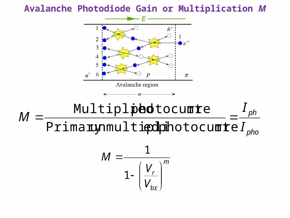
Avalanche Photodiode Gain or Multiplication M
pho
ph
I
IM
ntphotocurre edunmultipliPrimary
ntphotocurre Multiplied
m
r
VV
M
br
1
1
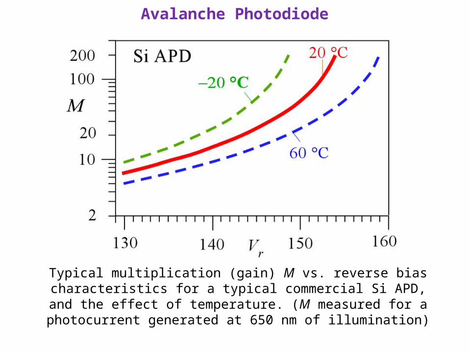
Avalanche Photodiode
Typical multiplication (gain) M vs. reverse bias characteristics for a typical commercial Si APD, and the effect of temperature. (M measured
for a photocurrent generated at 650 nm of illumination)

Avalanche Photodiode
(a) A Si APD structure without a guard ring. (b) A schematic illustration of the structure of a more practical Si APD. Note: SiO2 is silicon dioxide
and serves as an insulating passivation layer.

Photodiode Comparison
Photodiode l range lpeak R at lpeak
Gain Id For 1 mm2 Features
nm nm A/W GaP pin 150-550 450 0.1 <1 1 nm UV detectiona
GaAsP pn 150-750 500-720 0.2-0.4 <1 0.005-0.1 nA UV to visible, covering the human eye, low Id.
GaAs pin 570-870 850 0.5-0.5 <1 0.1-1 nA High speed and low Id
Si pn 200-1100 600-900 0.5-0.6 <1 0.005-0.1 nA Inexpensive, general purpose, low Id
Si pin 300-1100 800-1000 0.5-0.6 <1 0.1-1 nA Faster than pnSi APD 400-1100 800-900 0.4-0.6b 10-103 1-10 nAc High gains and fastGe pin 700-1800 1500-1580 0.4-0.7 <1 0.1-1 mA IR detection, fast.Ge APD 700-1700 1500-1580 0.4-0.8b 10-20 1-10 mAc IR detection, fastInGaAs pin 800-1700 1500-1600 0.7-1 <1 1-50 nA Telecom, high speed, low Id
InGaAs APD 800-1700 1500-1600 0.7-0.95b 10-20 0.05-10 mAc Telecom, high speed and gain.
InAs pn 2-3.6 mm 3.0-3.5 mm 1-1.5 <1 >100 mA Photovoltaic mode. Normally cooled
InSb pn 4-5.5 mm 5 mm 3 <1 Large Photovoltaic mode. Normally cooled
NOTE: cFGAP71 (Thorlabs); aAt M = 1; cAt operating multiplication.

Avalanche Photodiode Gain or Multiplication M
Ionization coefficient ratio
ae = Aexp(-B/E) Chyoweth's law
Avalanche Photodiode Gain or Multiplication M
M = exp(aew)Ionization coefficient
kwk
kM
e
])1(exp[
1
Electrons only
Electrons and holes
k = ah / ae

Simplified schematic diagram of a separate absorption and multiplication (SAM) APD using a heterostructure based on InGaAs-InP. P and N refer to p and n -type
wider-bandgap semiconductor.
Heterojunction Photodiodes: SAM

Heterojunction Photodiodes: SAM
(a) Energy band diagrams for a SAM detector with a step junction between InP and InGaAs. There is a valence band step DEv from InGaAs to InP that slows hole entry into the InP layer.
(b) An interposing grading layer (InGaAsP) with an intermediate bandgap breaks DEv and makes it easier for the hole to pass to the InP layer for a detector with a graded junction between InP and InGaAs. This is the SAGM structure.

Heterojunction Photodiodes: SAM
Simplified schematic diagram of a more practical mesa-etched SAGM layered APD
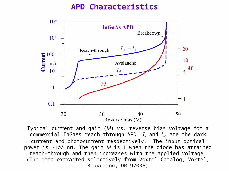
APD Characteristics
Typical current and gain (M) vs. reverse bias voltage for a commercial InGaAs reach-through APD. Id and Iph are the dark current and photocurrent respectively. The input optical
power is ~100 nW. The gain M is 1 when the diode has attained reach-through and then increases with the applied voltage. (The data extracted selectively from Voxtel Catalog,
Voxtel, Beaverton, OR 97006)
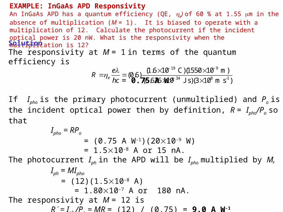
EXAMPLE: InGaAs APD ResponsivityAn InGaAs APD has a quantum efficiency (QE, he) of 60 % at 1.55 mm in the absence of multiplication (M = 1). It is biased to operate with a multiplication of 12. Calculate the photocurrent if the incident optical power is 20 nW. What is the responsivity when the multiplication is 12?
SolutionThe responsivity at M = 1 in terms of the quantum efficiency is
= 0.75 A W-1
If Ipho is the primary photocurrent (unmultiplied) and Po is the incident optical power then by definition, R = Ipho/Po so that
Ipho = RPo = (0.75 A W-1)(2010-9 W) = 1.510-8 A or 15 nA.
The photocurrent Iph in the APD will be Ipho multiplied by M,Iph = MIpho = (12)(1.510-8 A) = 1.8010-7 A or 180 nA.
The responsivity at M = 12 isR¢ = Iph /Po = MR = (12) / (0.75) = 9.0 A W-1
19 9
34 8 -1
(1.6 10 C)(1550 10 m)(0.6)
(6.626 10 J s)(3 10 m s )e
e
hc
R

EXAMPLE: Silicon APDA Si APD has a QE of 70 % at 830 nm in the absence of multiplication, that is M = 1. The APD is biased to operate with a multiplication of 100. If the incident optical power is 10 nW what is the photocurrent?
SolutionThe unmultiplied responsivity is given by,
= 0.47 A W-1
The unmultiplied primary photocurrent from the definition of R is
Ipho = RPo = (0.47 A W-1)(1010-9 W) = 4.7 nA
The multiplied photocurrent is
Iph = MIpho = (100)(4.67 nA ) = 470 nA or 0.47 mA
19 9
34 8 -1
(1.6 10 C)(830 10 m)(0.70)
(6.626 10 J s)(3 10 m s )e
e
hc
R
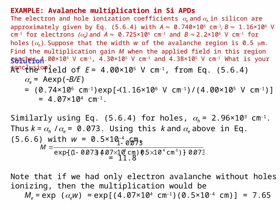
EXAMPLE: Avalanche multiplication in Si APDsThe electron and hole ionization coefficients ae and ah in silicon are approximately given by Eq. (5.6.4) with A 0.740×106 cm-1, B 1.16×10⁶ V cm-1 for electrons (ae) and A 0.725×106 cm-1 and B 2.2×10⁶ V cm-
1 for holes (ah). Suppose that the width w of the avalanche region is 0.5 mm. Find the multiplication gain M when the applied field in this region reaches 4.00×10⁵ V cm-1, 4.30×10⁵ V cm-1 and 4.38×10⁵ V cm-1
.
What is your conclusion? SolutionAt the field of E = 4.00×10⁵ V cm-1, from Eq. (5.6.4)
ae = Aexp(-B/E)= (0.74×106 cm-1)exp[-(1.16×10⁶ V cm-1)/(4.00×105 V cm-1)] =
4.07×104 cm-1.
Similarly using Eq. (5.6.4) for holes, ah = 2.96×103 cm-1. Thus k = ah /ae = 0.073. Using this k and ae above in Eq. (5.6.6) with w = 0.5×10⁻⁴ cm,
= 11.8
Note that if we had only electron avalanche without holes ionizing, then the multiplication would be
Me = exp (aew) = exp[(4.07×104 cm-1)(0.5×10⁻⁴ cm)] = 7.65
073.0)]cm 105.0)(cm 1007.4)(073.01(exp[
073.011-44
M
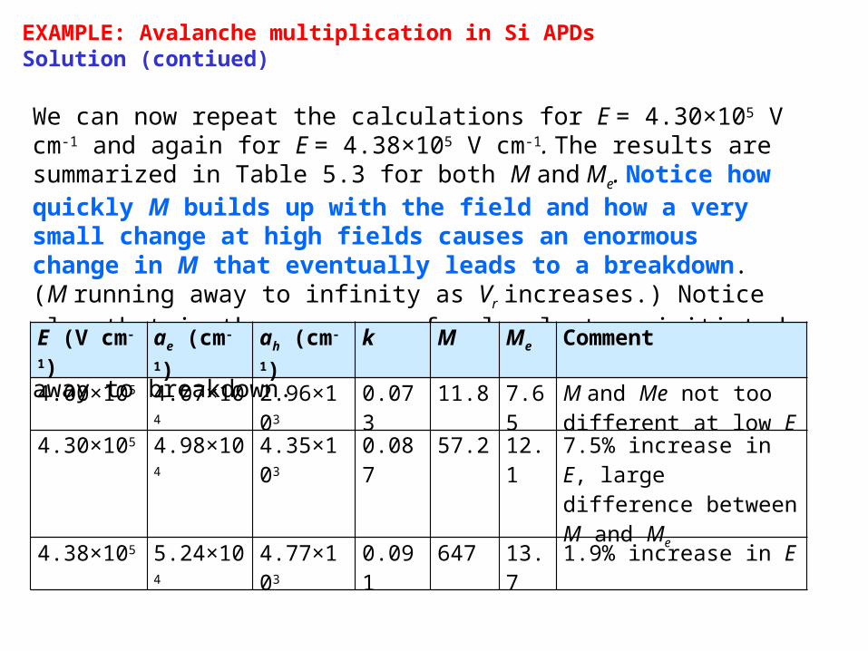
EXAMPLE: Avalanche multiplication in Si APDsSolution (contiued)
We can now repeat the calculations for E = 4.30×10⁵ V cm-1 and again for E = 4.38×10⁵ V cm-1. The results are summarized in Table 5.3 for both M and Me. Notice how quickly M builds up with the field and how a very small change at high fields causes an enormous change in M that eventually leads to a breakdown. (M running away to infinity as Vr increases.) Notice also that in the presence of only electron-initiated ionization, Me simply increases without a sharp run-away to breakdown.E (V cm-1) ae (cm-1) ah (cm-1) k M Me Comment
4.00×10⁵ 4.07×10⁴ 2.96×10³ 0.073 11.8 7.65 M and Me not too different at low E
4.30×10⁵ 4.98×10⁴ 4.35×10³ 0.087 57.2 12.1 7.5% increase in E, large difference between M and Me
4.38×10⁵ 5.24×10⁴ 4.77×10³ 0.091 647 13.7 1.9% increase in E

Superlattice APDMultiple Quantum Well Detectors
(a) Energy band diagram of a MQW superlattice APD.(b) Energy band diagram with an applied field and impact ionization.

Schottky Junction Photodiodes
GaAsP Schottky junction photodiode for 190-680
nm detection, from UV to red (Courtesy of
Hamamatsu)
GaP Schottky junction photodiode for 190 nm to 550 nm detection.
(Courtesy of Hamamatsu)
Schottky kunction type metal-semiconductor-metal (MSM) type photodetectors. (Courtesy of Hamamatsu)
AlGaN Scottky junction photodiode for UV
detection (Courtesy of sglux, Germany)

Schottky Junction
(a) Metal and an n-type semiconductor before contact. The metal work function Fm is greater than that of the n-type semiconductor (b) A Schottky junction forms between the
metal and the semiconductor. There is a depletion region in the semiconductor next to the metal and a built-in field Eo (c) Typical I vs. V characteristics of a Schottky contact device.
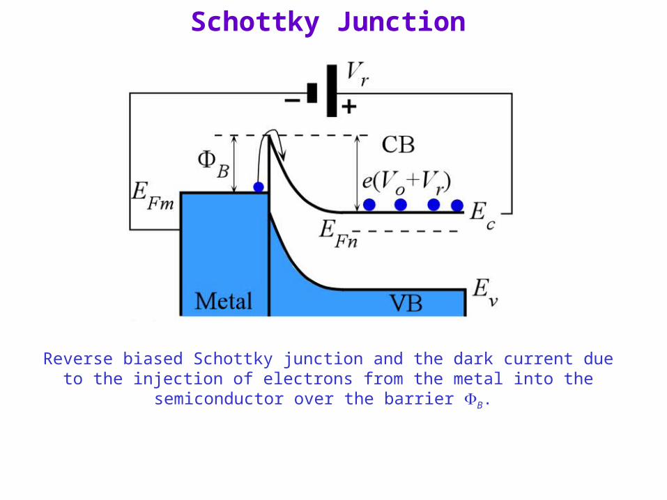
Reverse biased Schottky junction and the dark current due to the injection of electrons from the metal into the semiconductor over the barrier FB.
Schottky Junction

LEFT: Photogeneration in the depletion region and the resulting photocurrent. RIGHT: The Schottky junction photodetector
Schottky Junction

Schottky Junction Photodiodes
Schottky junctionl range
nm
Rpeak (at peak)
(A/W)
Jdark
per mm2Features with typical values
GaAsP 190-680 0.18 (610 nm) 5 pA UV to red, tR = 3.5 ms. (G1126 seriesa)
GaP 190-550 0.12 (440 nm) 5 pA UV to green, tR = 5 ms. (G1961a)
AlGaN 220-375 0.13 (350 nm) 1 pA Measurement of UV; blind to visible light. (AG38Sb)
GaAs 320-900 0.2 (830 nm) ~ 1 nAWide bandwidth > 10 GHz, tR < 30 ps. (UPD-30-VSG-Pc)
InGaAs MSM 850-1650 0.4 (1300 nm) 5 mAOptical high speed measurements, tR = 80 ps, tF = 160 ps. (G7096a)
GaAs MSM 450-870 0.3 (850 nm) 0.1 nAOptical high speed measurements, tR = 30 ps, tF = 30 ps. (G4176a)
Schottky junction based photodetectors and some of their features. tR and tF are the rise and fall times of the output of the photodetector for an optical pulse input. The rise and fall times represent the times
required for the output to rise from 10% to 90% of its final steady state value and to fall from 90% to 10% of its value before the optical pulse is turned off.
aHamamatsu (Japan); bsglux (Germany); cAlphalas
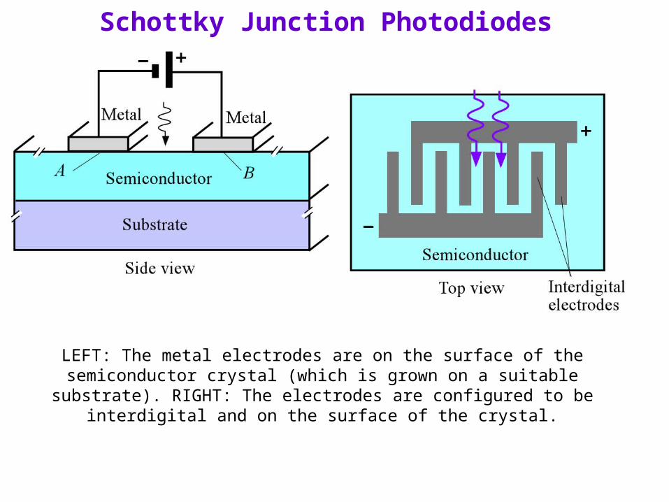
Schottky Junction Photodiodes
LEFT: The metal electrodes are on the surface of the semiconductor crystal (which is grown on a suitable substrate). RIGHT: The electrodes are configured to be
interdigital and on the surface of the crystal.

Schottky Junction Photodiodes
LEFT: Two neighboring Schottky junctions are connected end-to-end, but in opposite directions as shown for A and B. The energy band diagram without any bias is
symmetrical. The grey areas represent the SCL1 and SCL2 at A and B. RIGHT: Under a sufficiently large bias, the SCL1 from A extends and meets that from B so that the whole semiconductor between the electrodes is depleted. There is a large field in this region, and the photogenerated EHPs become separated and then drifted, which results in a
photocurrent.

Phototransistor
IE exp(eVBE/kBT)
Iph bIpho
Transistor action
Gain

Photoconductive Detectors
PbS (lead sulfide) photoconductive detectors for the detection of IR radiation up to 2.9 mm. They are typically used in such applications as radiation thermometers, flame monitors, water content and food
ingredient analyzers, spectrophotometers etc.. (P9217 series) (Courtesy of Hamamatsu.)

Photoconductive Detectors
A semiconductor slab of length l, width w and depth d is illuminated with
light of wavelength l
Photoconductive Detectors
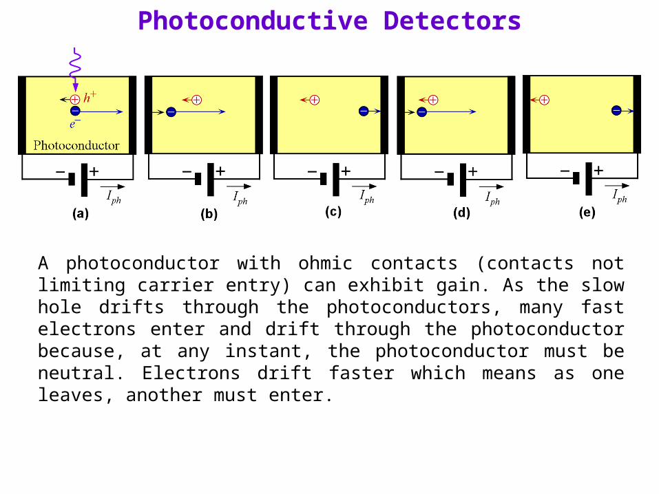
A photoconductor with ohmic contacts (contacts not limiting carrier entry) can exhibit gain. As the slow hole drifts through the photoconductors, many fast electrons enter and drift through the photoconductor because, at any instant, the photoconductor must be neutral. Electrons drift faster which means as one leaves, another must enter.

Photoconductivity D s and Photocurrent Density Jph
Steady state illumination
hcddhv
Ad
Ai
ii
II
g
phph
Photon flux = Fph
0ph
n
dt
ndg
hi = Internal quantum efficiency
Ds = emeDn + emhDp = eDn(me + mh)Photoconductivity
hcd
e hei )(
I E V
J ph
Photogeneration rate

Photoconductive Gain
Photon flux = Fph
hc
w
e
wdJ
e
Ihei EI )(
flow electron of Rate phph
hcwwd i I
gg phph )()Volume(generation electron of Rate
Photoconductive gain G
E)(
absorptionlight by generationelectron of Rate
circuit externalin flowelectron of Rate heG

Photoconductive Gain
Photon flux = Fph
E)(
absorptionlight by generationelectron of Rate
circuit externalin flowelectron of Rate heG
Electron and hole transit times (time to cross the semiconductor) are
te = l / (meE)
th = l / (mhE)
e
h
ehe tttG
1
Electron
Hole
Photoconductive gain G

Basic Photodiode Circuits
(a) The photodiode is reverse biased through RL and illuminated. Definitions of positive I and V are shown as if the photodiode were forward biased. (b) I-V characteristics of the photodiode with
positive I and V definitions in (a). The load line represents the behavior of the load R. The operating point is P where the current and voltage are I and V.

Basic Photodiode Circuits: The Load Line
The current through RL is
I = - (V + Vr) / RL
This is the load line shown in the figure. P is the intersection of the load line with the photodiode I vs. V curve and is the operating point.
P is the operating point
V = -3.5 V
I = - 2.5 m A
I Iph

Basic Photodiode Circuits
A simple circuit for the measurement of the photocurrent Iph by using a current-voltage converter or a transimpedance amplifier. The reverse bias Vr is a positive number. Note that biasing circuit for the op amp is not shown.

Photodiode Equivalent Circuit
(a) A real photodiode has series and parallel resistances Rs and Rp and a SCL capacitance Cdep. A and C represent anode and cathode terminals. (b) The equivalent circuit of a photodiodes. For ac (or transient) signals, the battery can be shorted since
ac signals will simply pass through the battery.

Reverse Biased Photodiode Equivalent Circuit
Rs = Series resistance
Rp = Shunt (parallel) resistance
Ideal photodiode
Total capacitance = ideal photodiode SCL capacitance + terminal capacitance

Cutoff Frequency fc
V(t)
The cutoff frequency or the bandwidth of the PD
tLtLstc CRCRRCR
f 2
1
)(2
1
2
1
eq
Req is equivalent resistance and represents (Rs + RL) in parallel with Rp
AssumptionDrift time of carriers is much less than 1/fc.Response is not limited by drift and diffusion times of caries within the device.

A Commercial Photoreceiver
A photoreceiver that has an InGaAs APD and peripheral electronics (ICs) to achieve high gain and high sensitivity. There is also a thermoelectric cooler (TEC) and a
temperature sensor (TSense). Courtesy of Voxtel Inc (www.voxtel-inc.com)
APD
Thermoelectric (TEC) cooler
Op amp
Output
APD bias Temperature sensor (Tsense)
TEC Current in direction
TEC Current out direction
Base/Collector
Emitterr
Op amp bias
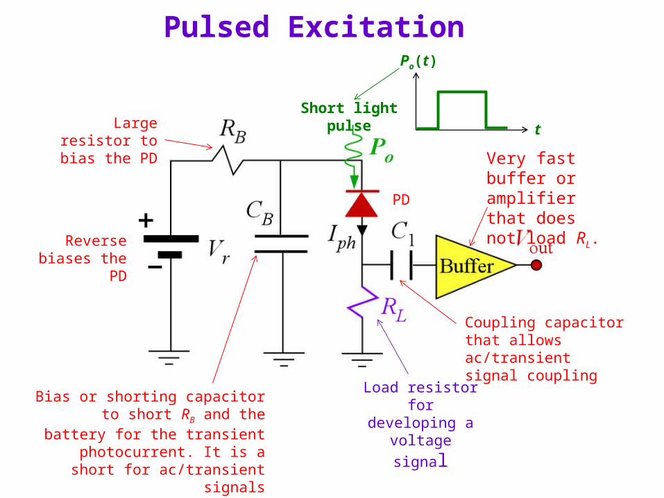
Pulsed Excitation
Large resistor to bias the PD
Bias or shorting capacitor to short RB and the battery for the transient
photocurrent. It is a short for ac/transient signals
Load resistor for developing a
voltage signal
Very fast buffer or amplifier that does not load RL.
Po(t)
t
Coupling capacitor that allows ac/transient signal coupling
Reverse biases the PD
PD
Short light pulse

Pulsed Excitation
Rise time Fall time
Assume: The buffer is extremely fast and does not limit the response
The Experiment
Are these related to fc?

Rise and Fall Times, and Bandwidth
Rise time Fall timeVery roughly, tR tF
V(t) V100exp(-t/t)
Measured from toff
tF = 2.2
= (Rs+ RL)Ct RLCt
= (Rs+ RL)Ct RLCt
)ns(
MHz35035.0
2
1
2
1
FFtLc CR
f
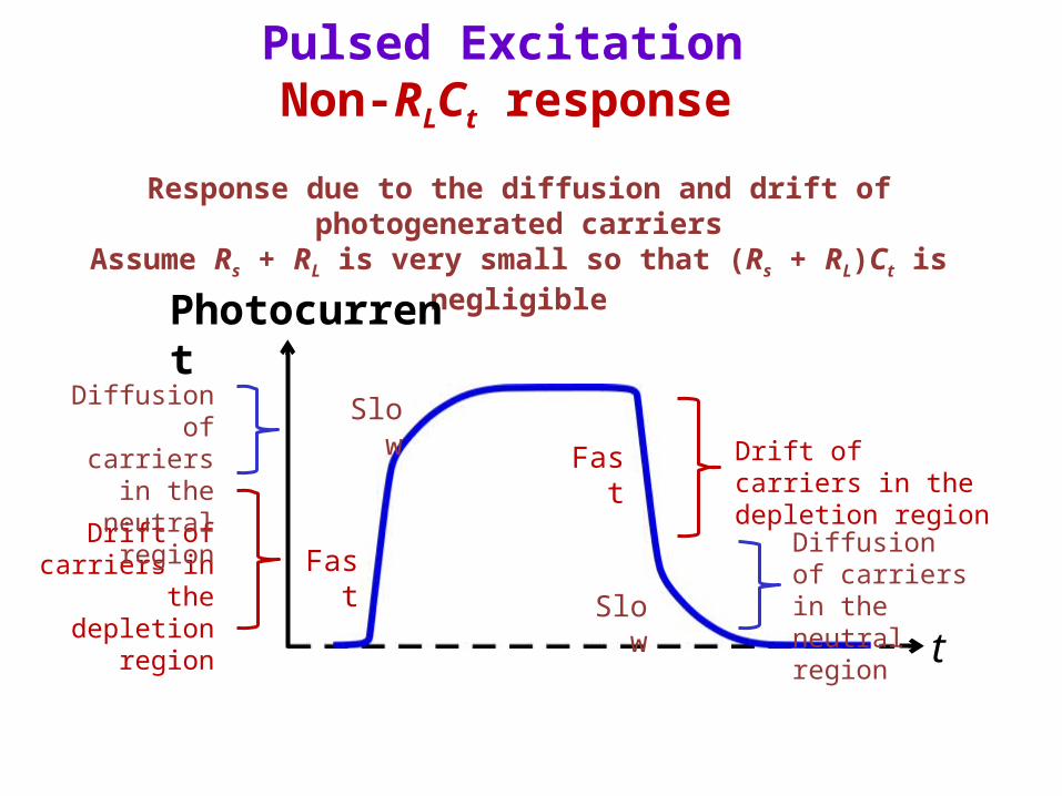
Pulsed ExcitationNon-RLCt response
Response due to the diffusion and drift of photogenerated carriersAssume Rs + RL is very small so that (Rs + RL)Ct is negligible
Drift of carriers in the depletion
region
Diffusion of carriers in the neutral region
Slow
Fast
Fast
Slow
t
Photocurrent
Drift of carriers in the depletion region
Diffusion of carriers in the neutral region

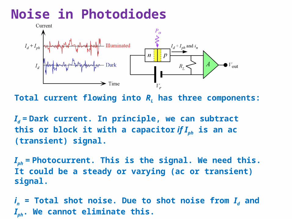
Noise in Photodiodes
Noise current = Total RMS current fluctuations
Constant illumination
What is the RMS of fluctuations?
Consider a receiver with a photodiode and a sampling resistor RL The amplifier A is assumed noiseless
Consider constant illumination Po
Total current without noise = Dark current (Id) + Photocurrent (Iph) = “Constant”
Observed Current = Dark current + Photocurrent and Fluctuations (Noise)
What is this “Noise” ?
2)(nsfluctuatio of RMS tiWe can represent the “noise current” by the RMS of fluctuations
i(t)

Noise in Photodiodes
The dark current has shot noise or fluctuations about Id,
in-dark = (2eIdB)1/2
Quantum noise is due to the photon nature of light and its effects are the same as shot noise. Photocurrent has quantum noise or shot noise
B = Bandwidth
in-quantum = (2eIphB)1/2
Noise current = Total RMS current fluctuations
Constant illumination
What is the RMS of fluctuations?
i(t)

Noise in Photodiodes
2quantum
2dark
2 nnn iii
Total shot noise current, in
in = [2e(Id + Iph)B]1/2
We can conceptually view the photodetector current as
Id + Iph + inThis flows through a load resistor RL and voltage across RL is amplified by A to
give Vout
The noise voltage (RMS) due to shot noise in PD = inRLA
Noise in Photodiodes
Total current flowing into RL has three components:
Id = Dark current. In principle, we can subtract this or block it with a capacitor if Iph is an ac (transient) signal.
Iph = Photocurrent. This is the signal. We need this. It could be a steady or varying (ac or transient) signal.
in = Total shot noise. Due to shot noise from Id and Iph. We cannot eliminate this.

Noise in Photodiodes
4
= fromcurrent noise Thermal1/2
th
L
BL R
TBkRi
4 =2 TBk iR BL i2 LRi inCurrent
The resistor RL exhibits thermal noise (Johnson noise)
Power in thermal fluctuations in RL = 4kBTB

Summary of Noise in PD and RL
Important Note: Total noise is always found by first summing the average powers involved in individual fluctuations e.g. power in shot noise + power in thermal noise
Power in shot noise in PD = in2RL = [2e(Id + Iph)B]RL
Power in thermal fluctuations in RL = 4kBTB
Noise in the amplifier A must also be includedSee advanced textbooks

PowerNoise
PowerSignalSNR
L
Bphd
ph
BLn
Lph
RTBk
BIIe
I
TBkRi
RI4
)(24SNR
2
2
2
Important Note: Total noise is always found by first summing the average powers involved in individual fluctuations e.g. power in shot noise + power in thermal noise
Signal to Noise Ratio

Noise Equivalent Power: NEP
2/11
Bandwidth
1SNRforpowerInputNEP
B
P
Definition
NEP is defined as the required optical input power to achieve a SNR of 1 within a bandwidth of 1 Hz
2/1
2/11 )(2
1NEP phd IIe
B
P
R
Units for NEP are W Hz–1/2

Detectivity, D
NEP
1yDetectivit
Definition
Specific detectivity D*
NEP*
2/1AD
Units for D* are cm Hz-1/2 W-1, or Jones

NEP and Detectivity of Photodetectors
PhotodiodeGaP
Schottky
Si
pin
Ge
pin
InGaAs
pin
PbS (PC)
-10C
PbSe (PC)
-10 C
InSb (PC)
-10C
lpeak (mm) 0.44 0.96 1.5 1.55 2.4 4.1 5.5
Id or Rd 10 pA 0.4 nA 3 mA 5 nA 0.1-1 MW 0.1-1 MW 1-10 kW
NEP W Hz-1/2 5.4×10⁻¹⁵ 1.6×10⁻¹⁴ 1×10-12 4×10-14 - -
D* cm Hz1/2/ W 1×10¹³ 1×10¹² 1×10¹¹ 5×10¹² 1×10⁹ 5×10⁹ 1×10⁹
Typical noise characteristics of a few selected commercial photodetectors. PC means a photoconductive detector, whose photoconductivity is used to detect light. For PC detectors,
what is important is the dark resistance Rd, which depends on the temperature.
2/1
2/11 )(2
1NEP phd IIe
B
P
R


