Average Model for PWM switch. Averaging Circuit Equations of PWM Switch. where. Averaging Power Stage Dynamics. Average Model for PWM Switch. Continuous Duty Ratio. Averaging Power Stage Dynamics. Continuous Duty Ratio. Averaging Power Stage Dynamics. Buck Converter Example. - PowerPoint PPT Presentation
22
1 Average Model for PWM switch ● Averaging Circuit Equations of PWM Switch () () () () () () cp ap cp ap ap a c a c c v v q t v v qt v qt i i qt i i qt i qt where ● Average Model for PWM Switch cp ap a c () () v v dt i i dt Averaging Power Stage Dynamics
Transcript
1
Average Model for PWM switch
● Averaging Circuit Equations of PWM Switch
( ) ( ) ( )
( ) ( ) ( )
cp ap cp ap ap
a c a c c
v v q t v v q t v q t
i i q t i i q t i q t
where
● Average Model for PWM Switch
cp ap
a c
( )
( )
v v d t
i i d t
Ave
rag
ing
Po
we
r S
tage
Dyn
am
ics
2
Continuous Duty Ratio
Continuous Duty Ratio
1( ) ( )
s
t
t Tsd t q t dt
T
( )q t
kd
( )d t
( 1) sk T skT ( 1) sk T ( 2) sk T
1
3
1
3
1
0
2
3
2
3
Ave
rag
ing
Po
we
r S
tage
Dyn
am
ics
3
Continuous Duty Ratio
SV 1
Ave
rag
ing
Po
we
r S
tage
Dyn
am
ics
( )d t
( )q t
1
0
0
1
( ) ( )s
t
t Tsd t q t dt
T
4
Buck Converter Example
ci
cp
vap
v
ai
SV
apv
SV
cpvSdT Sd T 0 V SdT Sd T 0 A
ai
Ci
Ave
rag
ing
Po
we
r S
tage
Dyn
am
ics
5
Implication of Average Model
1 : ( )d t
( )q t
( )d t
( )q t
1
0
0
Ave
rag
ing
Po
we
r S
tage
Dyn
am
ics
6
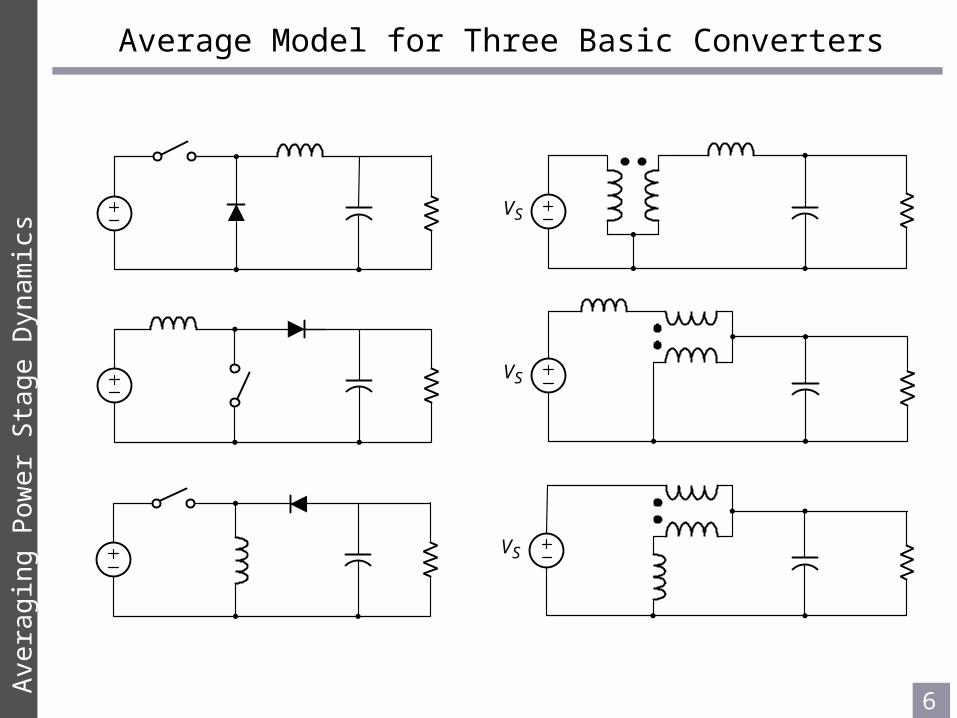
Average Model for Three Basic Converters
SV
SV
SV
Ave
rag
ing
Po
we
r S
tage
Dyn
am
ics
7
Linearization of Nonlinear FunctionL
ine
ariz
ing
Ave
rag
ed
Po
we
r S
tag
e D
ynam
ics
Y
y ( )f xy
X
x
x
y
ˆ
ˆ
ˆ
ˆ
x X
y (x) with x X x with
y: mall signal gain of nonlinear function
x x
x
f
fs
8
Linearization of simple Algebraic Equation
● For simple algebraic nonlinear equations, the small-signal model can be found by
1) Evaluating the nonlinear equation with the variables consisting of the dc and ac components 2) Equating only the ac component of the input and output variables in the resulting expression.
Lin
ear
izin
g A
vera
ge
d P
ow
er
Sta
ge D
yna
mic
s
ˆ ˆ ˆ ˆ
x 2x 2
2 2 2
i) 4x
ii) Y y ( X x ) X 2Xx x
f2x
2
Slope at x 2
● Example: small-signal gain of y=x2 evaluated at x=2
9
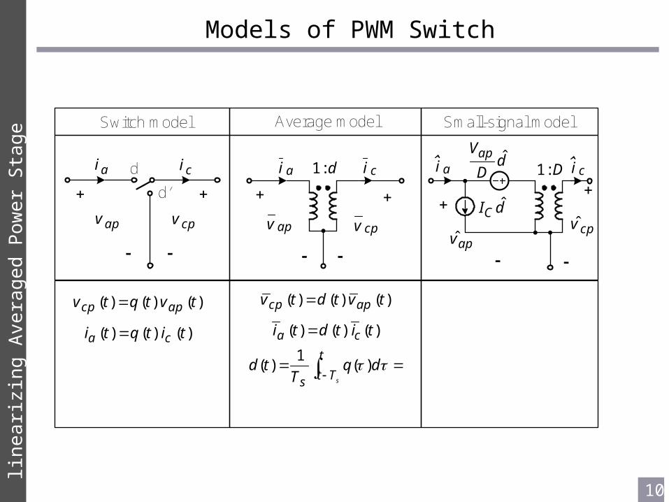
Small-signal Model for PWM Switch Model
a a
p p
c cai ci ai ci
ap ˆVd
D 1 : D1 : d
cp
vap
v ˆ
CI d
cp ap
a c
v d v
i d i
a c c
apap ap ap ap( )
ˆ ˆ
ˆ ˆˆ ˆ ˆ
i I d D i
vv v d D Dv v d
D● Small-signal modeling
ˆ ˆ ˆ ˆ ˆ ˆˆ
ˆˆ ˆ
ˆ ˆˆ ˆ
a c a a c c c c c c
cp ap ap cp ap cp
ap ap ap ap
( ) ( )( )
( ) ( )( )
i di I i D d I i DI di Di di
v d v v v D d v v
DV dV Dv dv
line
ariz
ing
Ave
rag
ed
Po
we
r S
tag
e D
ynam
ics
10
ˆapV dD
ˆCI d
Switch model Average model Small-signal model
d
d′
ai ci
apv cpv
( ) ( ) ( )cp apv t q t v t
( ) ( ) ( )a ci t q t i t
( ) ( ) ( )cp apv t d t v t
( ) ( ) ( )a ci t d t i t
1
( ) ( )s
t
t Tsd t q d
T
ˆcpv
ˆapv
cpvapv
ai ciciai 1: d 1:D
Models of PWM Switchlin
ear
izin
g A
vera
ge
d P
ow
er
Sta
ge
Dyn
amic
s
11
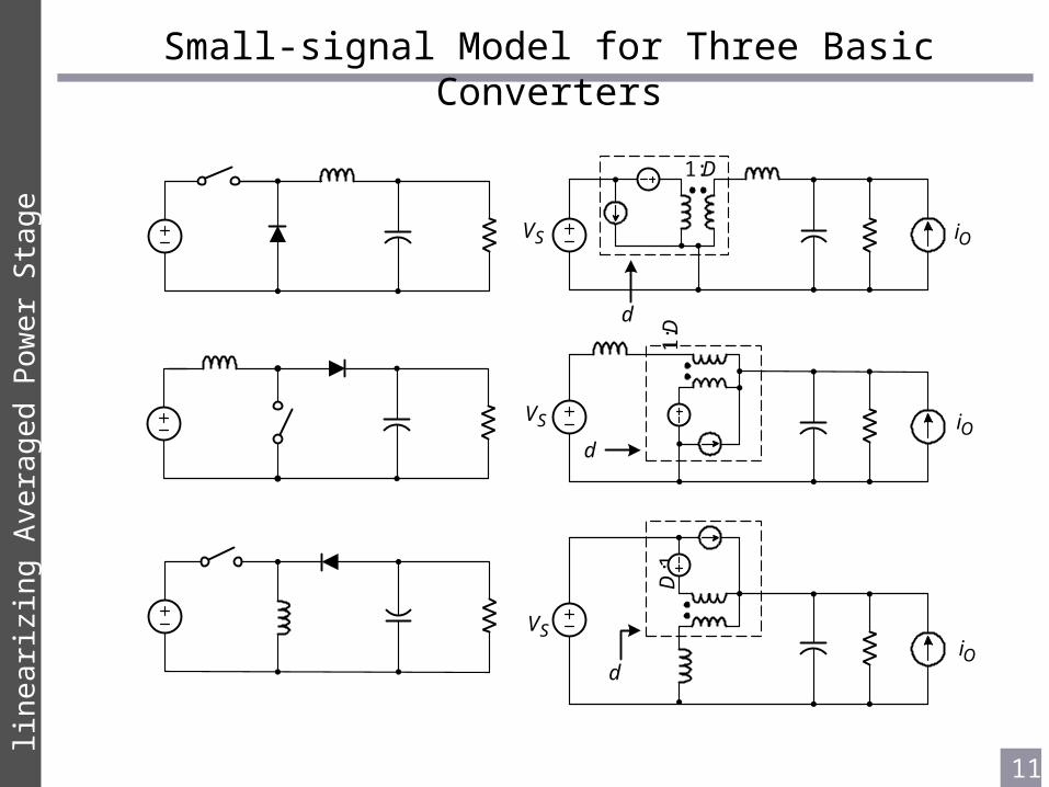
SV
1:D
1:D
:1D
Oi
d
SV
SV
d
d
Oi
Oi
Small-signal Model for Three Basic Converterslin
ear
izin
g A
vera
ge
d P
ow
er
Sta
ge
Dyn
amic
s
12
( )Sv s
( )Sv s
( )Sv s
1:D
( )Oi s
( )Oi s
( )Oi s
R
R
R
1
sC
1
sC
1
sC
sL
sL
sL
( )d s
( )d s
( )d s
S-domain Representation of Small-signal Modellin
ear
izin
g A
vera
ge
d P
ow
er
Sta
ge
Dyn
amic
s
13
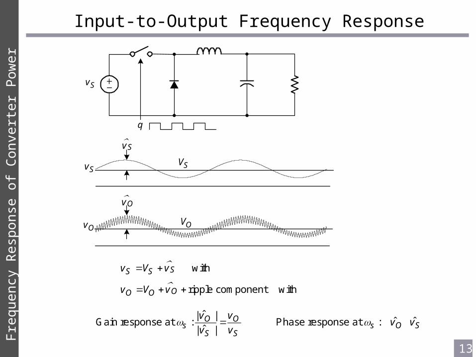
with
ripple component with
SS S
OO O
v V v
v V v
q
Sv
Ov
SV
OV
Sv
Ov
ˆ| |
ˆ ˆGain response at : Phase response at :ˆ| |O O
s s O SS S
v vv v
v v
Sv
Input-to-Output Frequency ResponseF
requ
enc
y R
esp
onse
of C
on
vert
er
Po
we
r S
tag
e
14
( )d t
Ov
D
OVOv
Gain response at : Phase response at :s s
( )q t
d
1
0
ripple component OO Ov V v
( )q t
SV
Duty ratio-to-Output Frequency ResponseF
requ
enc
y R
esp
onse
of C
on
vert
er
Po
we
r S
tag
e
15
100 1k 10k 100k-30
-20
-10
0
10
20
30
Gai
n [
dB
]
100 1k 10k 100k-120
-100
-80
-60
-40
-20
0
Ph
as
e [
de
g]
Frequency [Hz]
100 1k 10k 100k-30
-20
-10
0
10
20
30
100 1k 10k 100k-120
-100
-80
-60
-40
-20
0
Frequency [Hz]
Bode Plot Representation of Frequency Response F
requ
enc
y R
esp
onse
of C
on
vert
er
Po
we
r S
tag
e
16
( )Sv s ( )Ov s
s-domain Small-signal Model
● Input-to-Output Transfer Function:
● Input-to-Output Frequency Response
Fre
que
ncy
Res
pon
se o
f Co
nve
rte
r P
ow
er
Sta
ge
17
( )Ov s
( )Sv s
1:D
( )Oi sRC
L
( )d s
Li ( )Sv d s
D
| |vdG 2 2
( )( )
( ) 1 / /
O Svd
o o
Vv sG s
d s s Q s
2 2
( )( )
( ) 1 / /
Ovs
S o o
v s DG s
v s s Q s
2
2 2( )
( )( ) 1 / /
Op
O o o
v s sZ s
i s s Q s
| |vsG
| |pZ
Buck Converter ExampleF
requ
enc
y R
esp
onse
of C
on
vert
er
Po
we
r S
tag
e
18
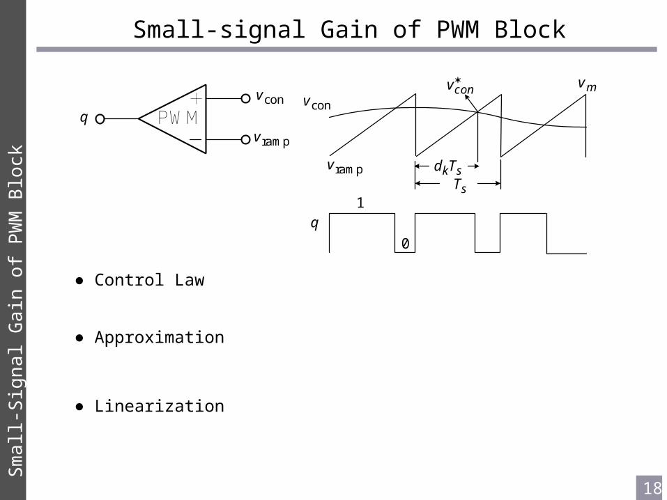
PWMconv
q
sTk sd T
conv
rampv
mvconv
q1
0
rampv
Small-signal Gain of PWM Block
● Control Law
● Approximation
● Linearization
Sm
all-
Sig
nal G
ain
of P
WM
Blo
ck
19
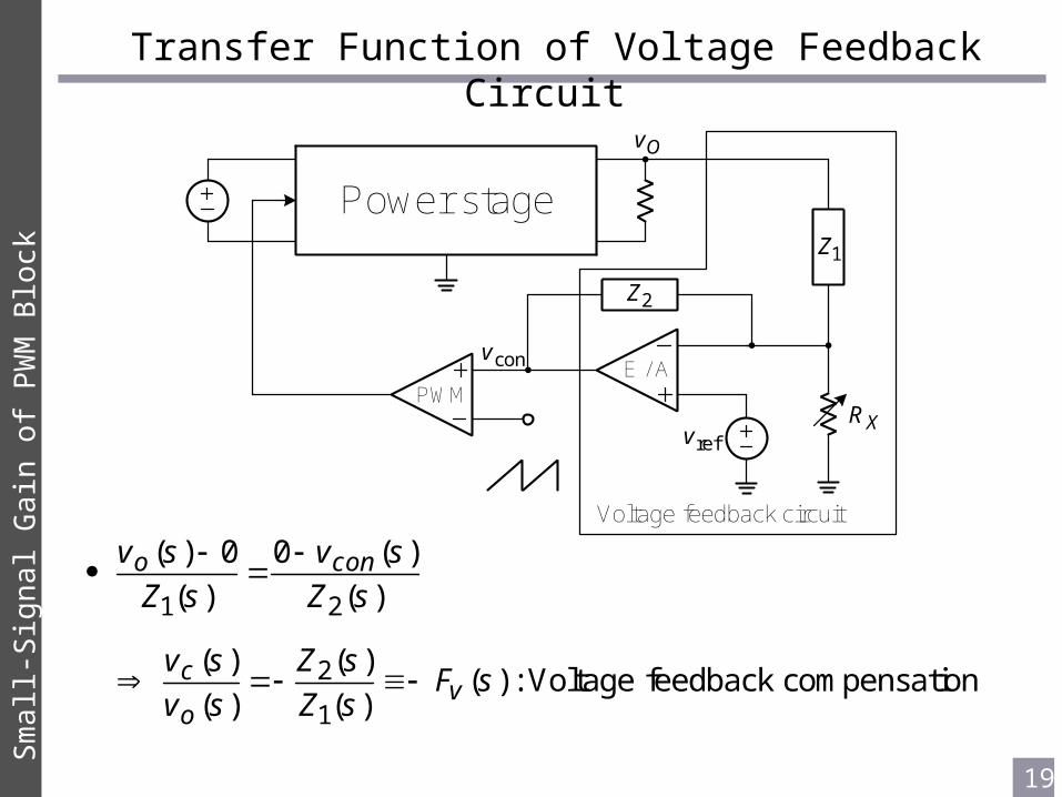
Transfer Function of Voltage Feedback Circuit
Voltage feedback circuit
Power stage
PWME / A
1Z
2Z
conv
refvXR
Ov
Sm
all-
Sig
nal G
ain
of P
WM
Blo
ck
1 2
2
1
( ) 0 0 ( )
( ) ( )
( ) ( )( ) :
( ) ( )Voltage feedback compensation
o con
cv
o
v s v s
Z s Z s
v s Z sF s
v s Z s
20
PWME / A
aX c′ Z
p
Y
1Z
2Z
General Circuit Diagram for Three Basic PWM ConvertersS


![A Novel Three-phase Three-Switch Three-Level High Power ......In [l] a three-phase three-switch three-level boost-type PWM rectifier system (cf. Fig.1) has been proposed which shows](https://static.documents.pub/doc/80x56/5fac53daf3633c2f9b66b17f/a-novel-three-phase-three-switch-three-level-high-power-in-l-a-three-phase.jpg)