25
Basic Bipolar Process Description • Bipolar Process Flow – Vertical npn – Lateral pnp – JFET – Prepared by Randy Geiger, September 2001
| Date post: | 24-Dec-2015 |
| Category: |
Documents |
| Upload: | victoria-marilynn-marshall |
| View: | 247 times |
| Download: | 1 times |

Basic Bipolar Process Description
• Bipolar Process Flow– Vertical npn– Lateral pnp– JFET
– Prepared by Randy Geiger, September 2001
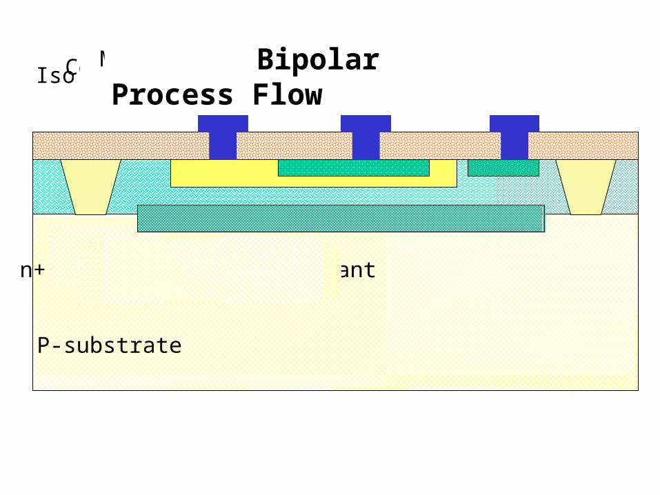
Bipolar Process Flow
P-substrate
n+ buried collector implant
n-epitaxy
Buried collector
Isolation Diffusionp-base diffusion n+ emitter diffusionOxidationContact OpeningsMetalization Bipolar Process Flow
n+ buried collector implantBuried collector
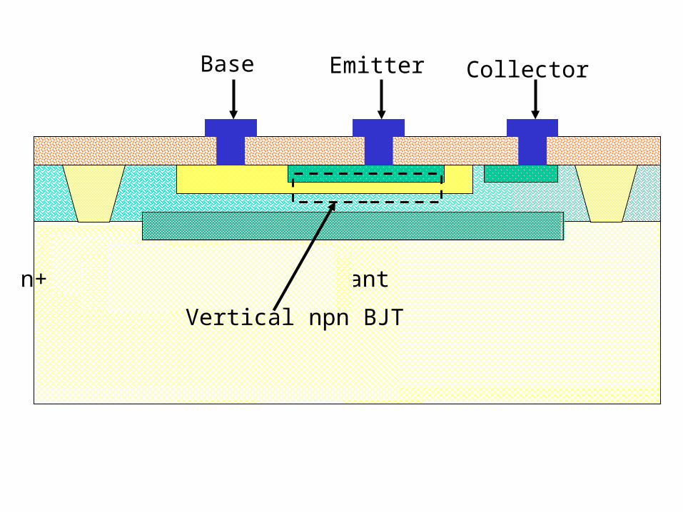
Base Emitter Collector
Vertical npn BJT

B E C
Lateral pnp Modification
E C B
Lateral pnp BJT

B E C
JFET Modification
S DG

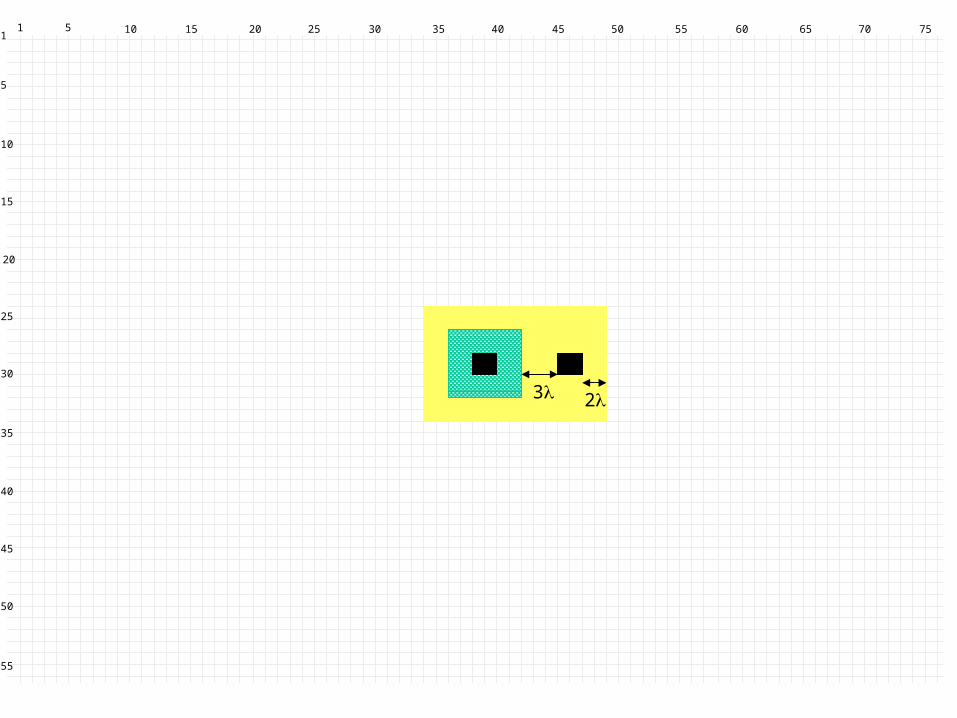
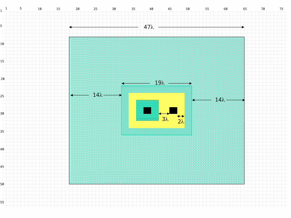
BJT Layout and Area Issues
• BJT Layout
• BJT Area Requirements
• Comparison of Area between MOS and Bipolar Processes

1 5 10 15 20 25 30 35 40 45 50 6055 7065 751
5
10
20
15
30
25
40
35
50
45
55

1 5 10 15 20 25 30 35 40 45 50 6055 7065 751
5
10
20
15
30
25
40
35
50
45
55
3
1 5 10 15 20 25 30 35 40 45 50 6055 7065 751
5
10
20
15
30
25
40
35
50
45
55
3 2

1 5 10 15 20 25 30 35 40 45 50 6055 7065 751
5
10
20
15
30
25
40
35
50
45
55
3 2
15

1 5 10 15 20 25 30 35 40 45 50 6055 7065 751
5
10
20
15
30
25
40
35
50
45
55
3 2
19
2

1 5 10 15 20 25 30 35 40 45 50 6055 7065 751
5
10
20
15
30
25
40
35
50
45
55
3 2
19
14 14
43

1 5 10 15 20 25 30 35 40 45 50 6055 7065 751
5
10
20
15
30
25
40
35
50
45
55
3 2
19
14 14
43
14
1 5 10 15 20 25 30 35 40 45 50 6055 7065 751
5
10
20
15
30
25
40
35
50
45
55
3 2
19
14
47
14

1 5 10 15 20 25 30 35 40 45 50 6055 7065 751
5
10
20
15
30
25
40
35
50
45
55
3 2
19
14
47
14
4
1 5 10 15 20 25 30 35 40 45 50 6055 7065 751
5
10
20
15
30
25
40
35
50
45
55
3 2
14
47
14
46
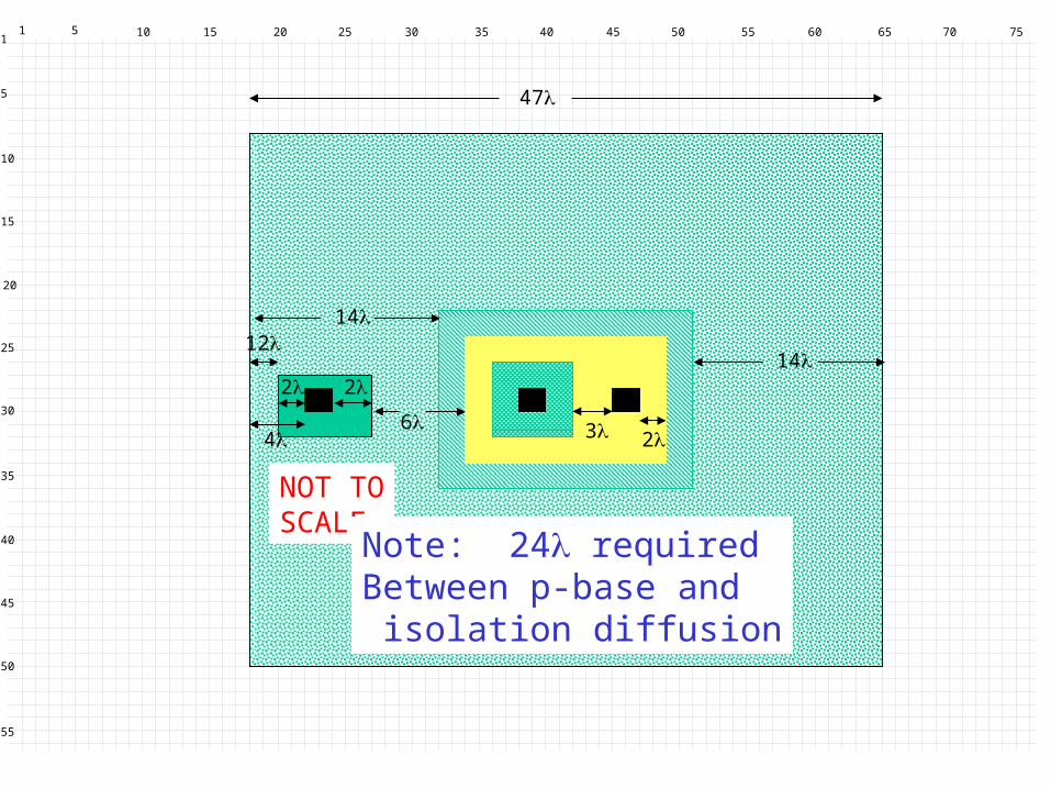
12
22
NOT TOSCALE
Note: 24 requiredBetween p-base and isolation diffusion
1 5 10 15 20 25 30 35 40 45 50 6055 7065 751
5
10
20
15
30
25
40
35
50
45
55
3 2
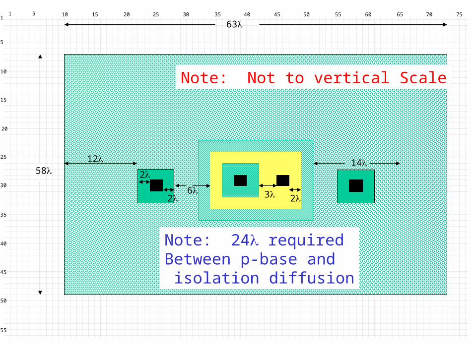
14
63
6
12
2
2
Note: 24 requiredBetween p-base and isolation diffusion
Note: Not to vertical Scale
58
1 5 10 15 20 25 30 35 40 45 50 6055 7065 751
5
10
20
15
30
25
40
35
50
45
55
3 2
14
63
6
12
2
2
Note: 24 requiredBetween p-base and isolation diffusion
Note: Not to vertical Scale
58

1 5 10 15 20 25 30 35 40 45 50 6055 7065 751
5
10
20
15
30
25
40
35
50
45
55
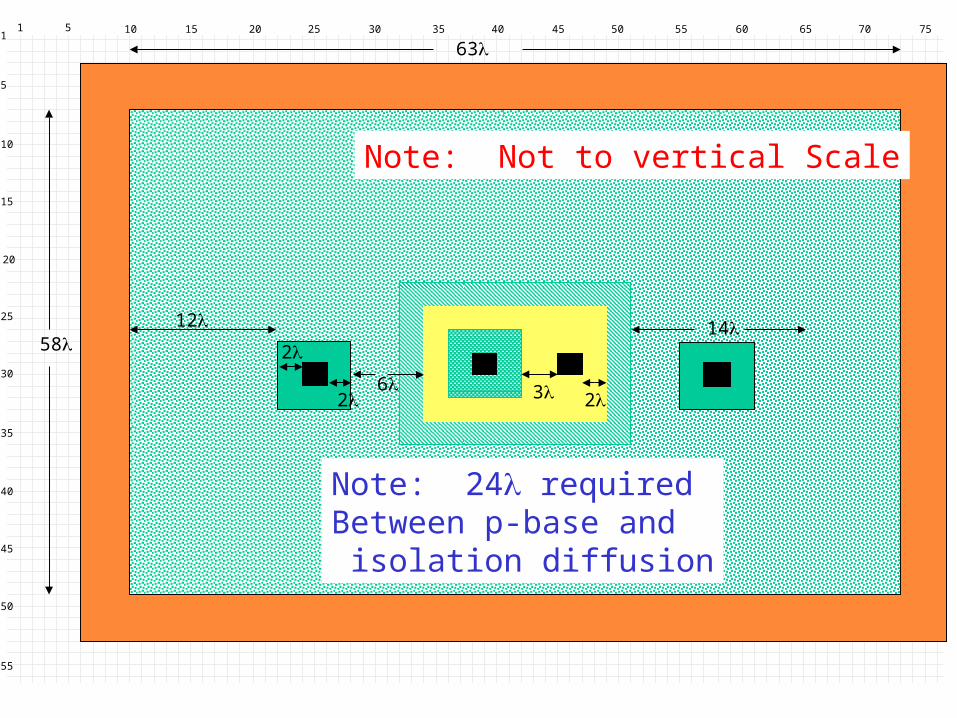
63
Note: Not to vertical Scale
58
67
62
1 5 10 15 20 25 30 35 40 45 50 6055 7065 751
5
10
20
15
30
25
40
35
50
45
55
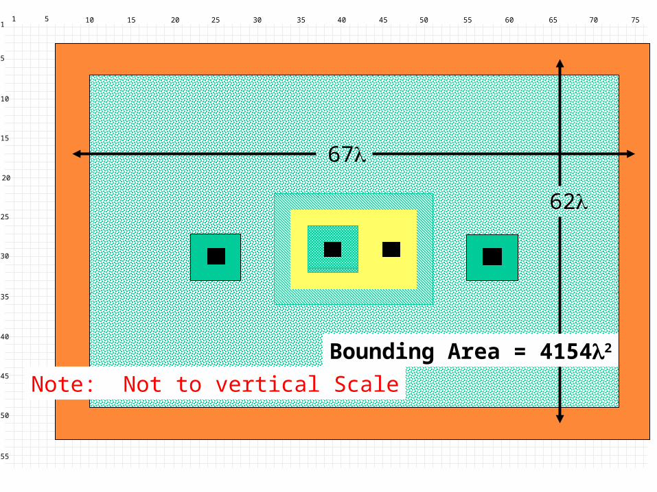
Note: Not to vertical Scale
67
62
Bounding Area = 41542

1 5 10 15 20 25 30 35 40 45 50 6055 7065 751
5
10
20
15
30
25
40
35
50
45
55
16
13
Bounding Area = 208
Comparison with Area for n-channel MOSFET in Bulk CMOS

1 5 10 15 20 25 30 35 40 45 50 6055 7065 751
5
10
20
15
30
25
40
35
50
45
55
14
12
Bounding Area = 168
Active Area = 62
Minimum-Sized MOSFET

1 5 10 15 20 25 30 35 40 45 50 6055 7065 751
5
10
20
15
30
25
40
35
50
45
55
Note: Not to vertical Scale
67
62
MOSFET BJT
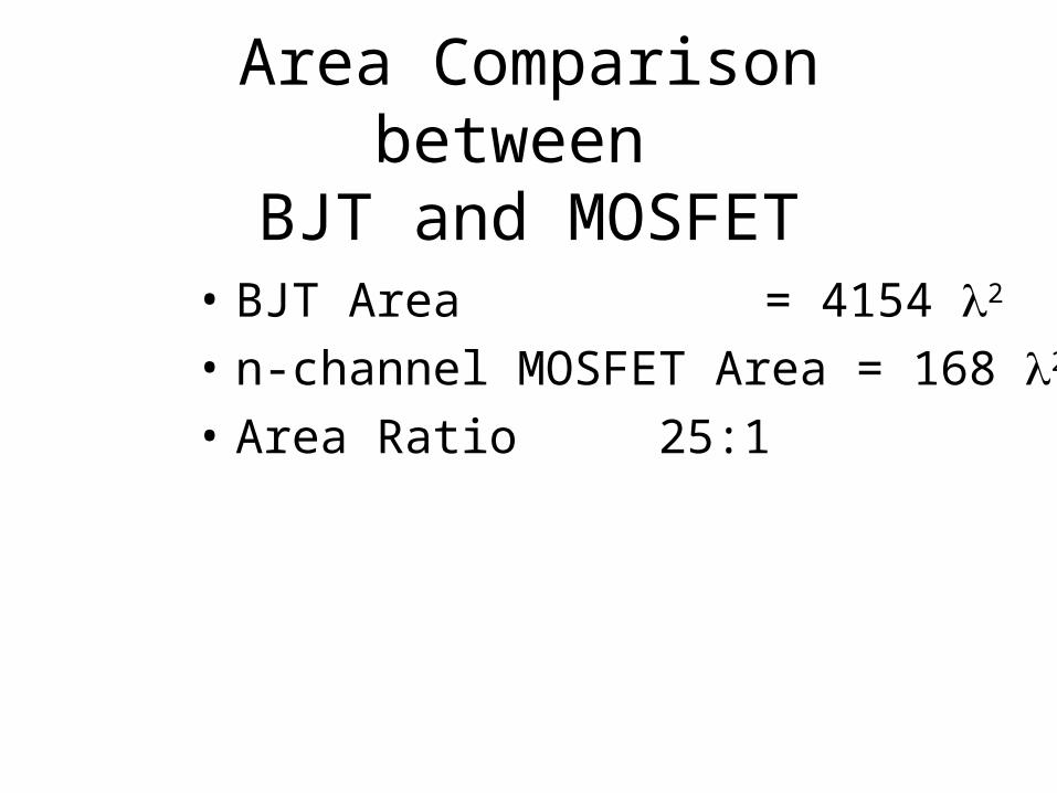
Area Comparison between BJT and MOSFET
• BJT Area = 4154 2
• n-channel MOSFET Area = 168 2
• Area Ratio 25:1

That’s all folks!


