2.0 BACKGROUND 2.1 Elements of Circuits 2.1.1 Transformer Fig.1: The Transformer A Transformer is an electrical device that transfers energy between two circuits through electromagnetic induction. A transformer may be used as a safe and efficient voltage converter to change the AC voltage at its input to a higher or lower voltage at its output without changing the frequency. Other uses include current conversion, isolation with or without changing voltage and impedance conversion. 4
Transcript
2.0 BACKGROUND
2.1 Elements of Circuits
2.1.1 Transformer
Fig.1: The Transformer
A Transformer is an electrical device that transfers energy between two circuits through
electromagnetic induction. A transformer may be used as a safe and efficient voltage converter to
change the AC voltage at its input to a higher or lower voltage at its output without changing the
frequency. Other uses include current conversion, isolation with or without changing voltage
and impedance conversion.
A transformer most commonly consists of two windings of wire that are wound around a
common core to provide tight electromagnetic coupling between the windings. The core material
is often a laminated iron core. The coil that receives the electrical input energy is referred to as
the primary winding; the output coil is the secondary winding.
Applications of Transformer: Transformers perform voltage conversion, isolation protection,
and impedance matching. In terms of voltage conversion, transformers can step up voltage and
4
step down current from generators to high voltage transmission lines, and step down voltage/step
up current to local distribution circuits or industrial customers. The step-up transformer is used to
increase the secondary voltage relative to the primary voltage. The step-down transformer is used
to decrease the secondary voltage relative to the primary voltage. Transformers range in size
from thumbnail-sized units used in microphones to those weighing hundreds of tons
interconnecting the power grid. A broad range of transformer designs are used in electronic and
electric power applications, including miniature, audio, isolation, high frequency, power
conversion, etc.
An isolation transformer is a transformer used to transfer electrical power from a source of
alternating current (AC) power to some equipment or device while isolating the powered device
from the power source, usually for safety reasons. Isolation transformers provide galvanic
isolation and are used to protect against electric shock, to suppress electrical noise in sensitive
devices, or to transfer power between two circuits that must not be connected. A transformer sold
for isolation is often built with special insulation between primary and secondary, and is
specified to withstand a high voltage between windings.
Isolation transformers block transmission of the DC component in signals from one circuit to the
other, but allow AC components in signals to pass. Transformers that have a ratio of 1 to 1
between the primary and secondary windings are often used to protect secondary circuits and
individuals from electrical shocks. Suitably designed isolation transformers block interference
caused by ground loops. Isolation transformers with electrostatic shields are used for power
supplies for sensitive equipment such as computers or laboratory instruments.
Isolation transformers are designed with attention to capacitive coupling between the two
windings. The capacitance between primary and secondary windings would also couple AC
5
current from the primary to the secondary. A grounded Faraday shield between the primary and
the secondary greatly reduces the coupling of common-mode noise. This may be another
winding or a metal strip surrounding a winding. Differential noise can magnetically couple from
the primary to the secondary of an isolation transformer, and must be filtered out if a problem.
The ideal transformer induces secondary voltage VS as a proportion of the primary voltage VP
and respective winding turns as given by the equation:
V P
V S=
NP
N S=a (1)
where
a: is the winding turns ratio
V P: is t h e primary voltage
V S : is t he secondary voltage
The power losses due to transformer could be found by
W h ≈ η βmax1.6 (2)
Hysteresis loss is obtained by:
Ph=ηW h=η . f βmax1.6 (3)
Where f is the frequency, η is the hysteresis coefficient and βmax is the maximum flux density.
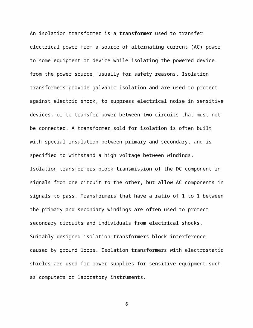
2.1.2 Diode
Diode is an electrical device allowing current to move through it in one direction with far
greater ease than in the other. Semiconductor diode is considered as the most common kind of
diode in modern circuit design. The schematic diagram of diode is shown in Figure 2 below.
6
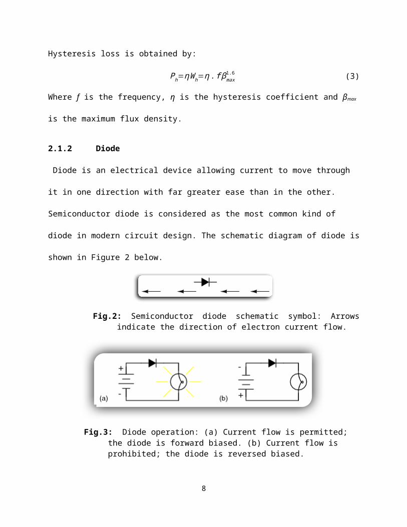
Fig.2: Semiconductor diode schematic symbol: Arrows indicate the direction of electron current flow.
Fig.3: Diode operation: (a) Current flow is permitted; the diode is forward biased. (b) Current flow is prohibited; the diode is reversed biased.
When the polarity of the battery is such that electrons are allowed to flow through the diode, the
diode is said to be forward-biased. Conversely, when the battery is “backward” and the diode
blocks current, the diode is said to be reverse-biased. A diode may be thought of as like a switch:
“closed” when forward-biased and “open” when reverse-biased as shown in Figure 3.
2.1.3 Optocoupler
An optical coupler, also called opto-isolator, optocoupler, opto coupler, photocoupler or optical
isolator, is a passive optical component that can combine or split transmission data (optical
power) from optical fibers. It is an electronic device which is designed to transfer electrical
signals by using light waves in order to provide coupling with electrical isolation between its
input and output. The main purpose of an optocoupler is to prevent rapidly changing voltages or
high voltages on one side of a circuit from distorting transmissions or damaging components on
the other side of the circuit. An optocoupler contains a light source often near an LED which
converts electrical input signal into light, a closed optical channel and a photosensor, which
detects incoming light and either modulates electric current flowing from an external power
7
supply or generates electric energy directly. The sensor can either be a photoresistor, a silicon-
controlled rectifier, a photodiode, a phototransistor or a triac. A schematic diagram for
optocoupler is shown in Figure 4 below.
Fig. 4: Schematic diagram for optocoupler.
Types of Optocouplers
There are many different kinds of optocouplers and at Future Electronics we stock many of the
most common types categorized by number of channels, operating temperature, output voltage,
isolation voltage, packaging type and current transfer ratio (CTR). The parametric filters on our
website can help refine your search results depending on the required specifications.
The most common sizes for maximum output voltage are 30 V, 70 V and 80 V. We also carry
optocouplers with a maximum output voltage up to 80 kV. The maximum operating temperature
can range from 70 oC to 150 oC, with the most common opto coupler chips having a maximum
operating temperature of 100 oC.
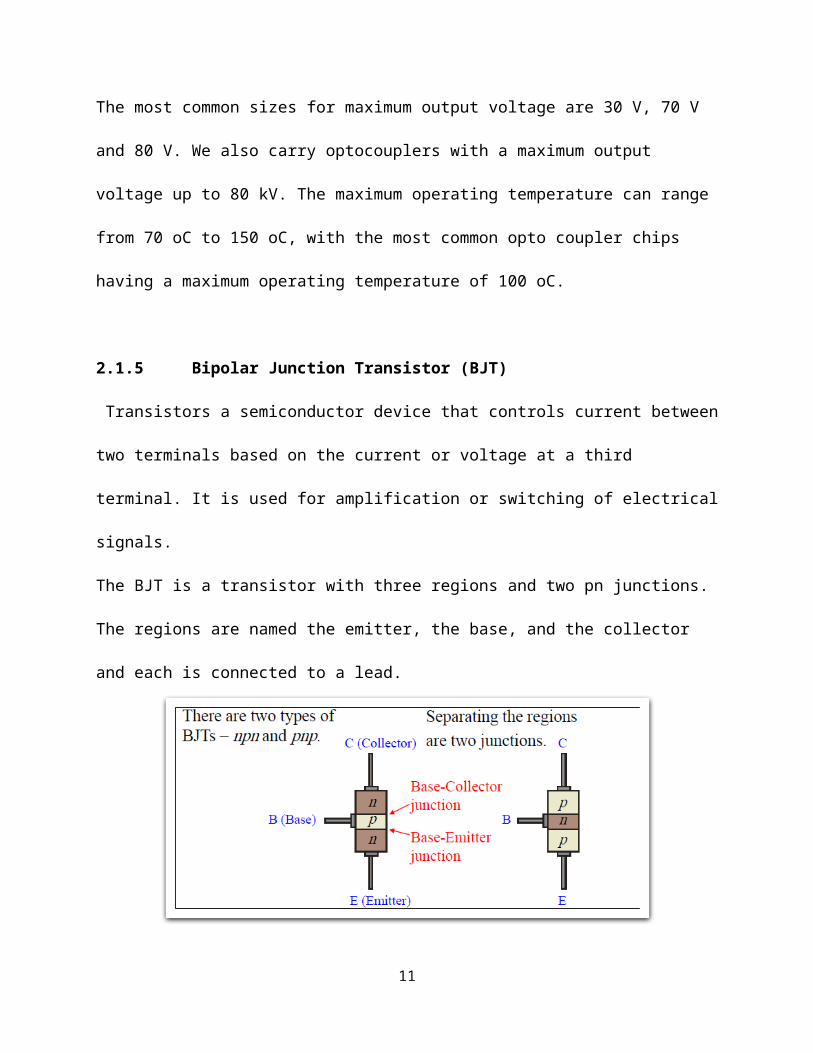
2.1.5 Bipolar Junction Transistor (BJT)
Transistors a semiconductor device that controls current between two terminals based on the
current or voltage at a third terminal. It is used for amplification or switching of electrical
signals.
8
The BJT is a transistor with three regions and two pn junctions. The regions are named the
emitter, the base, and the collector and each is connected to a lead.
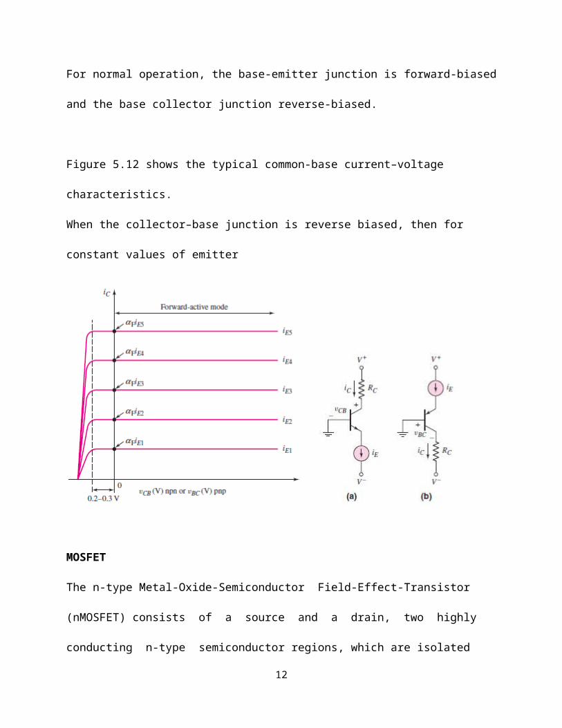
For normal operation, the base-emitter junction is forward-biased and the base collector junction
reverse-biased.
Figure 5.12 shows the typical common-base current–voltage characteristics.
When the collector–base junction is reverse biased, then for constant values of emitter
9
MOSFET
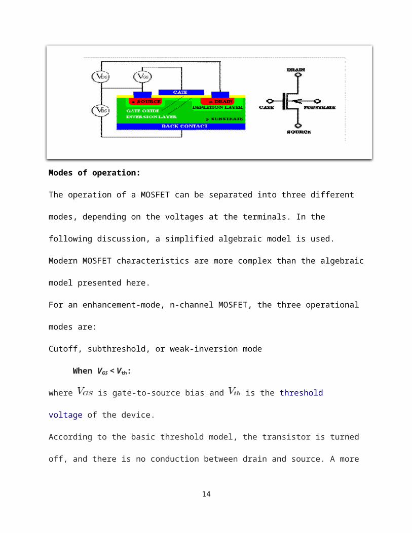
The n-type Metal-Oxide-Semiconductor Field-Effect-Transistor (nMOSFET) consists of a
source and a drain, two highly conducting n-type semiconductor regions, which are isolated
from the p-type substrate by reversed-biased p-n diodes. A metal or poly-crystalline gate covers
the region between source and drain. The gate is separated from the semiconductor by the gate
oxide [4]. The basic structure of an n-type MOSFET and the corresponding circuit symbol are
shown in Figure 2.
10
Modes of operation:
The operation of a MOSFET can be separated into three different modes, depending on the
voltages at the terminals. In the following discussion, a simplified algebraic model is used.
Modern MOSFET characteristics are more complex than the algebraic model presented here.
For an enhancement-mode, n-channel MOSFET, the three operational modes are:
Cutoff, subthreshold, or weak-inversion mode
When VGS < Vth:
where is gate-to-source bias and is the threshold voltage of the device.
According to the basic threshold model, the transistor is turned off, and there is no conduction
between drain and source. A more accurate model considers the effect of thermal energy on
the Fermi–Dirac distribution of electron energies which allow some of the more energetic
electrons at the source to enter the channel and flow to the drain. This results in a subthreshold
current that is an exponential function of gate–source voltage. While the current between drain
and source should ideally be zero when the transistor is being used as a turned-off switch, there
is a weak-inversion current, sometimes called subthreshold leakage.
Triode mode or linear region (also known as the ohmic mode
When VGS > Vth and VDS < ( VGS – Vth )
11
The transistor is turned on, and a channel has been created which allows current to flow between
the drain and the source. The MOSFET operates like a resistor, controlled by the gate voltage
relative to both the source and drain voltages.The current from drain to source is modeled as:
I D=μn CoxWL ((V GS−V th) V DS−
V DS2
2 )where is the charge-carrier effective mobility, is the gate width, is the gate length
and is the gate oxide capacitance per unit area.
Saturation or active mode:
The switch is turned on, and a channel has been created, which allows current to flow between
the drain and source. Since the drain voltage is higher than the source voltage, the electrons
spread out, and conduction is not through a narrow channel but through a broader, two- or three-
dimensional current distribution extending away from the interface and deeper in the substrate.
The onset of this region is also known as pinch-off to indicate the lack of channel region near the
drain. Although the channel does not extend the full length of the device, the electric field
between the drain and the channel is very high, and conduction continues.
MOSFET Critical Parameters
When switch mode operation of the MOSFET is considered, the goal is to switch between the
lowest and highest resistance states of the device in the shortest possible time. Since the practical
switching times of the MOSFETs (~10ns to 60ns) is at least two to three orders of magnitude
longer than the theoretical switching time (~50ps to200ps), it seems important to understand
12
the discrepancy. Referring back to the MOSFET models in Figure 2, note that all models include
three capacitors connected between the three terminals of the device. Ultimately, the switching
performance of the MOSFET transistor is determined by how quickly the voltages can be
changed across these capacitors.
Therefore, in high speed switching applications, the most important parameters are the parasitic
capacitances of the device. Two of these capacitors, the CGS and CGD capacitors
correspond to the actual geometry of the device while the CDS capacitor is the capacitance of the
base collector diode of the parasitic bipolar transistor (body diode).
When switch mode operation of the MOSFET is considered, the goal is to switch between the
lowest and highest resistance states of the device in the shortest possible time. Since the practical
switching times of the MOSFETs (~10ns to 60ns) is at least two to three orders of magnitude
longet r han the theoretical switching time (~50ps to200ps), it seems important to understand
the discrepancy. Referring back to the MOSFET models in Figure 2, note that all models include
three capacitors connected between the three terminals of the device. Ultimately, the switching
performance of the MOSFET transistor is determined by how quickly the voltages can be
changed across these capacitors.
Therefore, in high speed switching applications, the most important parameters are the parasitic
capacitances of the device. Two of these capacitors, the CGS and CGD capacitors
correspond to the actual geometry of the device while the CDS capacitor is the capacitance of the
base collector diode of the parasitic bipolar transistor (body diode).
13
The CGS capacitor is formed by the overlap of the source and channel region by the gate
electrode. Its value is defined by the actual geometry of the regions and stays constant (linear)
under different
operating conditions.
The CGD capacitor is the result of two effects. Part of it is the overlap of the JFET region and
the gate electrode in addition to the capacitance of the depletion region which is non-linear. The
equivalent CGD capacitance is a function of the drain source voltage of the device approximated
by the following formula:
CGD≈CGD ,0
1+K1 √V DS
Unfortunately, non of the above mentioned capacitance values are defined directly in the transistor data
sheets. Their values are given indirectly by the CISS, CRSS, and COSS capacitor values and must be
calculated as:
CGD = C RSS
CGS = C ISS − CRSS
CDS=C0 ss−C RSS
Further complication is caused by the CGD
Capacitor in switching applications because it is Placed in the feedback path between the input and
output of the device. Accordingly, its effective value in switching applications can be much larger
depending on the drain source voltage of the MOSFET. This phenomenon is called the “Miller” effect
14
and it can be expressed as:
CGD,equ=(1+gfs . RL) . CGD
Since the CGD and CDS capacitors are voltage dependent, the data sheet numbers are valid only at the
test conditions listed. The relevant average capacitances for a certain application have to be calculated
based on the required charge to establish the actual voltage change across the capacitors. For most
power MOSFETs the following approximations can be useful
CGD,avg=2.C RSS .√ V DS ,spec
V DS ,off
COSS ,avg=2.COSS ,spec √ V DS , spec
V DS , off
The next important parameter to mention is the gate mesh resistance, RG,I. This parasitic resistance
describes the resistance associated by the gate signal distribution within the device.its very important in
high speed switching cause it is in between the driver and the input capacitor of the device.
The transeconductance of the mosfet called “small gane in the linear region of its operation.” Its
important at which mosfet is turnd-on or off, the relationship between transconductance and drain current
and gate to source voltage is:
gfs=dI D
dV GS
The maximum current of the mosfet in the linear mode is :
15
I D=(V GS−V t h ) . g fs
SWITCHING APPLICATIONS
Now, that all the players are identified, let’s investigate the actual switching behavior of the
MOSFET transistors. To gain a better understanding of the fundamental procedure, the parasitic
inductances of the circuit will be neglected. Later their respective effects on the basic operation
will be analyzed individually. Furthermore, the following descriptions relate to clamped
inductive switching because most MOSFET transistors and high speed gate drive circuits used in
switch mode power supplies work in that operating mode.
Turn-On procedure
The turn-on event of the MOSFET transistor can be divided into four intervals as depicted in Figure 4.
16
In the first step the input capacitance of the device is charged from 0V to VTH. During this interval most
of the gate current is charging the CGS capacitor. A small current is flowing through the CGD capacitor
too. As the voltage increases at the gate terminal and the CGD capacitor’s voltage has to be slightly
reduced.
This period is called the turn-on delay, because both the drain current and the drain voltage of the device
remain unchanged.
This period is called the turn-on delay, because both the drain current and the drain voltage of the device
remain unchanged. Once the gate is charged to the threshold level, the MOSFET is ready to carry current.
In the second interval the gate is rising from VTH to the Miller plateau level, VGS,Miller. This is the
linear operation of the device when current is proportional to the gate voltage. On the gate side, current is
flowing into the CGS and CGD capacitors just like in the first time interval and the VGS voltage is
increasing. On the output side of the device, the drain current is increasing, while the drain-to-source
voltage stays at the previous level (VDS,OFF). This can be understood looking at the schematic in Figure
17
3. Until all the current is transferred into the MOSFET and the diode is turned-off completely to be able
to block reverse voltage across its pn junction, the drain voltage must stay at the output voltage level.
Entering into the third period of the turn-on procedure the gate is already charged to the sufficient voltage
(VGS,Miller) to carry the entire load current and the rectifier diode is turned off. That now allows the
drain voltage to fall. While the drain voltage falls across the device, the gate to- source voltage stays
steady. This is the Miller plateau region in the gate voltage waveform. All the gate current available from
the driver is diverted to discharge the CGD capacitor to facilitate the rapid voltage change across the
drain-to-source terminals. The drain current of the device stays constant since it is now limited by the
external circuitry, i.e. the DC current source.
The last step of the turn-on is to fully enhance the conducting channel of the MOSFET by applying a
higher gate drive voltage. The final amplitude of VGS determines the ultimate on-resistance of the device
during its on-time. Therefore, in this fourth interval, VGS is increased from VGS,Miller to its final value,
VDRV. This is accomplished by charging the CGS and CGD capacitors, thus gate current is now split
between the two components. While these capacitors are being charged, the drain current is still constant,
and the drain-to source voltage is slightly decreasing as the on resistance of the device is being reduced.
Turn-Off procedure
The description of the turn-off procedure for the MOSFET transistor is basically back tracking
the turn-on steps from the previous section. Start with VGS being equal to VDRV and the
current in the device is the full load current represented by IDC in Figure 3. The drain-to-source
voltage is being defined by IDC and the RDS(on) of the MOSFET. The four turn-off steps are
shown in Figure5. for completeness.
18
Figure 5. MOSFET turn-off time intervals
The first time interval is the turn-off delay which is required to discharge the CISS capacitance
from its initial value to the Miller plateau level. During this time the gate current is supplied by
the CISS capacitor itself and it is flowing through the CGS and CGD capacitors of the MOSFET.
The drain voltage of the device is slightly increasing as the overdrive voltage is diminishing. The
current in the drain is unchanged. In the second period, the drain-to-source voltage of the
MOSFET rises from ID⋅RDS(on) to the final VDS(off) level, where it is clamped to the output
voltage by the rectifier diode according to the simplified schematic of Figure 3. During this time
period – which corresponds to the Miller plateau in the gate voltage waveform - the gate current
19
is strictly the charging current of the CGD capacitor because the gate-to-source voltage is
constant. This current is provided by the bypass
capacitor of the power stage and it is subtracted from the drain current. The total drain current
still equals the load current, the beginning of the third time interval is signified by the turn-on of
the diode, thus providing an alternative route to the load current. The gate voltage resumes
falling from VGS,Miller to VTH. The majority of the gate current is coming out of the CGS
capacitor, because the CGD capacitor is virtually fully charged from the previous time interval.
The MOSFET is in linear operation and the declining gate-to-source voltage causes the drain
current to decrease and reach near zero by the end of this interval. Meanwhile the drain voltage is
steady at VDS(off) due to the forward biased rectifier diode. The last step of the turn-off
procedure is to fully discharge the input capacitors of the device. VGS is further reduced until it
reaches 0V. The bigger portion of the gate current, similarly to the third turn-off time interval,
supplied by the CGS capacitor. The drain current and the drain voltage in the device are
unchanged. Summarizing the results, it can be concluded that the MOSFET transistor can be
switched between its highest and lowest impedance states (either turn-on or turn-off) in four time
intervals. The lengths of all four time intervals are a function of the parasitic capacitance values,
the required voltage change across them and the available gate drive current. This emphasizes
the importance of the proper component selection and optimum gate drive design for high speed,
high frequency switching applications.
Characteristic numbers for turn-on, turn-off delays, rise and fall times of the MOSFET switching
waveforms are listed in the transistor data sheets. Unfortunately, these numbers correspond to the
specific test conditions and to resistive load, making the comparison of different manufacturers’
20
products difficult. Also, switching performance in practical applications with clamped inductive
load is significantly different from the numbers given in the data sheets.
PIC Microcontroller
The microcontrollers played revolutionary role in embedded industry after the invention of
Intel 8051. The steady and progressive research in this field gave the industry more efficient,
high-performance and low-power consumption microcontrollers. The AVR, PIC and ARM are
the prime examples. The new age microcontrollers are getting smarter and richer by including
latest communication protocols like USB, I2C, SPI, Ethernet, CAN etc.
History:
The PIC microcontroller was developed by General Instruments in 1975. PIC was developed when
Microelectronics Division of General Instruments was testing its 16-bit CPU CP1600. Although the
CP1600 was a good CPU but it had low I/O performance. The PIC controller was used to offload the I/O
the tasks from CPU to improve the overall performance of the system.
21
In 1985, General Instruments converted their Microelectronics Division to Microchip Technology. PIC
stands for Peripheral Interface Controller. The General Instruments used the acronyms Programmable
Interface Controller and Programmable Intelligent Computer for the initial PICs (PIC1640 and PIC1650).
In 1993, Microchip Technology launched the 8-bit PIC16C84 with EEPROM which could be
programmed using serial programming method. The improved version of PIC16C84 with flash memory
(PIC18F84 and PIC18F84A) hit the market in 1998.
Development:
Since 1998, Microchip Technology continuously developed new high performance microcontrollers with
new complex architecture and enhanced in-built peripherals. PIC microcontroller is based on Harvard
architecture. At present PIC microcontrollers are widely used for industrial purpose due to its high
performance ability at low power consumption. It is also very famous among hobbyists due to moderate
cost and easy availability of its supporting software and hardware tools like compilers, simulators,
debuggers etc.
PIC18F4520
CPU
Up to 10 MIPS Performance at 3V
C compiler optimized RISC architecture
22
8x8 Single Cycle Hardware Multiply
System
Internal oscillator support-31 kHz to 8MHz with 4xPLL
Fail-Safe Clock Monitor- allows safe shutdown if clock fails
Watchdog Timer with separate RC oscillator
Wide operating Voltage range; 2.0V to 5.5V
nanoWatt Power Managed Modes
Run, Idle and SLEEP modes
Idle mode currents down to 5.8uA typical
Sleep mode currents down to 0.1uA typical
Analog Features
10-bit ADC, 13 channels, 100K samples per second
Programmable Low Voltage Detection Module
Programmable Brown-out-Reset Module
Two Analog Comparators multiplexing
Peripherals
23
Master Synchronous Serial Port supports SPI™ and I2C™ master and slave mode