2• Controls Boost Preregulator to Near-UnityPower Factor AND MEDICAL APPLICATIONS
• Controlled Baseline• Limits Line Distortion• One Assembly/Test Site• World-Wide Line Operation• One Fabrication Site• Overvoltage Protection• Available in Military (–55°C/125°C)• Accurate Power Limiting
Temperature Range (1)
• Average Current Mode Control • Extended Product Life Cycle• Improved Noise Immunity • Extended Product-Change Notification• Improved Feed-Forward Line Regulation • Product Traceability• Leading Edge Modulation• 150-µA Typical Start-Up Current• Low-Power BiCMOS Operation• 12-V to 17-V Operation
(1) Additional temperature ranges are available - contact factory
The UCC2817 and UCC2818 provides all the functions necessary for active power-factor-correctedpreregulators. The controller achieves near-unity power factor by shaping the ac-input line current waveform tocorrespond to that of the ac input line voltage. Average current mode control maintains stable, low-distortionsinusoidal line current.
Designed with TI's BiCMOS process, the UCC2817 and UCC2818 offers new features, such as lower start-upcurrent, lower power dissipation, overvoltage protection, a shunt UVLO detect circuitry, a leading-edgemodulation technique to reduce ripple current in the bulk capacitor, and an improved, low-offset (±2-mV) currentamplifier to reduce distortion at light load conditions.
The UCC2817 offers an on-chip shunt regulator with low start-up current suitable for applications utilizing abootstrap supply. The UCC2818 is intended for applications with a fixed supply (VCC).
The devices are available in a 16-pin D package.
ORDERING INFORMATIONTA = TJ PACKAGE (1) ORDERABLE PART NUMBER TURN-ON THRESHOLD
–55°C to 125°C SOIC – D Reel UCC2818MDREP 10.2 V
(1) Package drawings, standard packing quantities, thermal data, symbolization, and PCB design guidelines are available atwww.ti.com/sc/package.
1
Please be aware that an important notice concerning availability, standard warranty, and use in critical applications of TexasInstruments semiconductor products and disclaimers thereto appears at the end of this data sheet.
CAI: Current amplifier noninverting input. Place a resistor between this pin and the GND side of current senseresistor. This input and the inverting input (MOUT) remain functional down to and below GND.
CAOUT: Current amplifier output. This is the output of a wide bandwidth operational amplifier that senses linecurrent and commands the PFC pulse-width modulator (PWM) to force the correct duty cycle. Compensationcomponents are placed between CAOUT and MOUT.
CT: Oscillator timing capacitor. A capacitor from CT to GND sets the PWM oscillator frequency according to:
The lead from the oscillator timing capacitor to GND should be as short and direct as possible.
DRVOUT: Gate drive. The output drive for the boost switch is a totem-pole MOSFET gate driver on DRVOUT.Use a series gate resistor to prevent interaction between the gate impedance and the output driver that mightcause the DRVOUT to overshoot excessively. See characteristic curve (Figure 13) to determine minimumrequired gate resister value. Some overshoot of the DRVOUT output is always expected when driving acapacitive load.
GND: Ground. All voltages measured with respect to ground. VCC and REF should be bypassed directly to GNDwith a 0.1-µF or larger ceramic capacitor.
IAC: Current proportional to input voltage. This input to the analog multiplier is a current proportional toinstantaneous line voltage. The multiplier is tailored for very low distortion from this current input (IIAC) tomultiplier output. The recommended maximum IIAC is 500 µA.
MOUT: Multiplier output and current amplifier inverting input. The output of the analog multiplier and the invertinginput of the current amplifier are connected together at MOUT. As the multiplier output is a current, this is ahigh-impedance input so the amplifier can be configured as a differential amplifier. This configuration improvesnoise immunity and allows for the leading-edge modulation operation. The multiplier output current is limited to (2× IIAC). The multiplier output current is given by the equation:
Where:
K = 1/V is the multiplier gain constant
OVP/EN: Over-voltage/enable. A window comparator input that disables the output driver if the boost outputvoltage is a programmed level above the nominal, or disables both the PFC output driver and resets SS if pulledbelow 1.9 V (typ).
PKLMT: PFC peak current limit. The threshold for peak limit is 0 V. Use a resistor divider from the negative sideof the current sense resistor to VREF to level shift this signal to a voltage level defined by the value of the senseresistor and the peak current limit. Peak current limit is reached when PKLMT voltage falls below 0 V.
RT: Oscillator charging current. A resistor from RT to GND is used to program oscillator charging current. Aresistor between 10 kΩ and 100 kΩ is recommended. Nominal voltage on this pin is 3 V.
SS: Soft-start. VSS is discharged for VVCC low conditions. When enabled, SS charges an external capacitor with acurrent source. This voltage is used as the voltage error signal during start-up, enabling the PWM duty cycle toincrease slowly. In the event of a VVCC dropout, the OVP/EN is forced below 1.9 V (typ), SS quickly discharges todisable the PWM.
Note: In an open-loop test circuit, grounding the SS pin does not ensure 0% duty cycle. Please see theapplication section for details.
VAOUT: Voltage amplifier output. This is the output of the operational amplifier that regulates output voltage. Thevoltage amplifier output is internally limited to approximately 5.5 V to prevent overshoot.
VCC: Positive supply voltage. Connect to a stable source of at least 20 mA between 10 V and 17 V for normaloperation. Bypass VCC directly to GND to absorb supply current spikes required to charge external MOSFET gatecapacitances. To prevent inadequate gate drive signals, the output devices are inhibited unless VVCC exceedsthe upper under-voltage lockout voltage threshold and remains above the lower threshold.
VFF: Feed-forward voltage. The RMS voltage signal generated at this pin by mirroring 1/2 of the IIAC into a singlepole external filter. At low line, the VFF voltage should be 1.4 V.
VSENSE: Voltage amplifier inverting input. This is normally connected to a compensation network and to theboost converter output through a divider network.
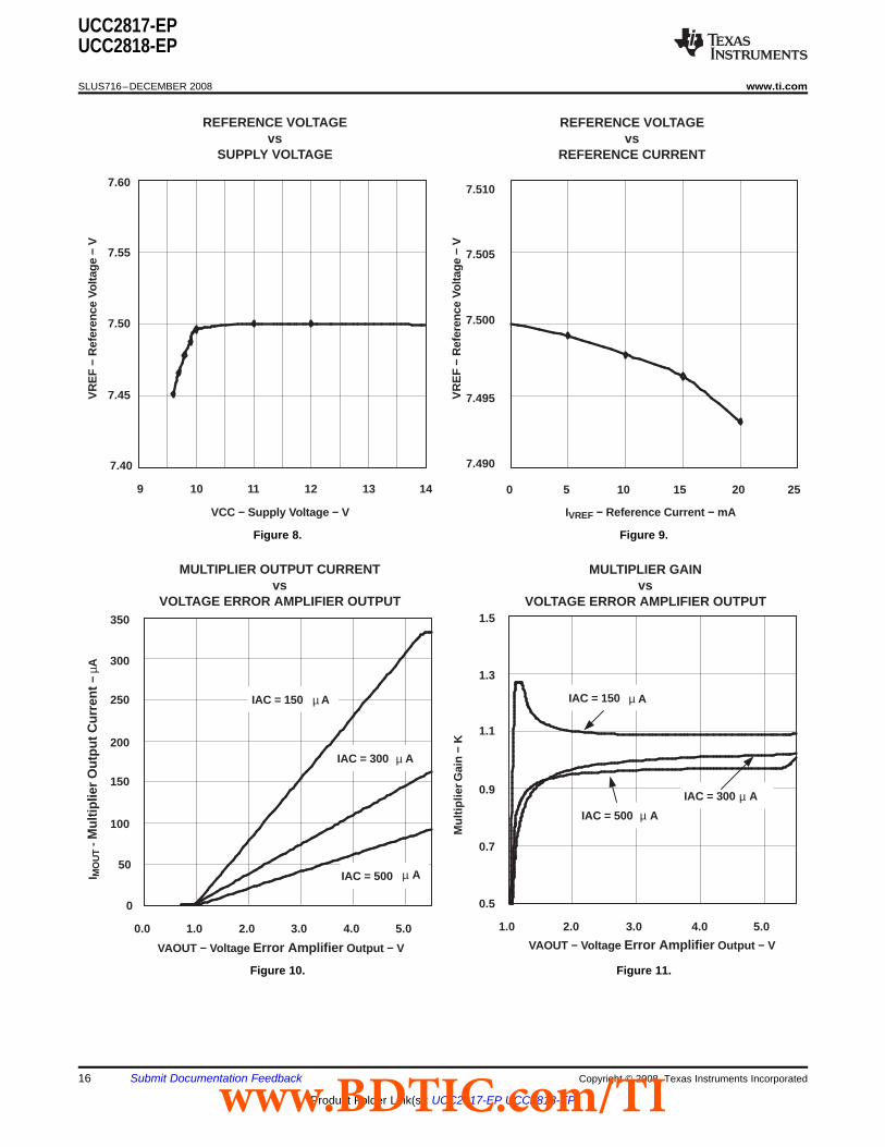
VREF: Voltage reference output. VREF is the output of an accurate 7.5-V voltage reference. This output iscapable of delivering 20 mA to peripheral circuitry and is internally short-circuit current limited. VREF is disabledand remains at 0 V when VVCC is below the UVLO threshold. Bypass VREF to GND with a 0.1-µF or largerceramic capacitor for best stability. Please refer to Figure 8 and Figure 9 for VREF line and load regulationcharacteristics.
over operating free-air temperature range (unless otherwise noted)
MIN MAX UNITVCC Supply voltage 18 VICC Supply current 20 mA
Gate drive current, continuous 0.2 AGate drive current 1.2 A
CAI, MOUT, SS 8Input voltage PKLMT 5 V
VSENSE, OVP/EN 10RT, IAC, PKLMT 10
Input current mAVCC (no switching) 20
Maximum negative voltage DRVOUT, PKLMT, MOUT –0.5 VPower dissipation 1 W
θJA Package thermal impedance °C/WTJ Junction temperature –55 150 °CTstg Storage temperature range –65 150 °CTsol Lead temperature Soldering, 10 s 300 °C
(1) Stresses beyond those listed under "absolute maximum ratings" may cause permanent damage to the device. These are stress ratingsonly, and functional operation of the device at these or any other conditions beyond those indicated under "recommended operatingconditions" is not implied. Exposure to absolute-maximum-rated conditions for extended periods may affect device reliability.
THERMAL RESISTANCEPACKAGE θJC(°C/W) θJA(°C/W)
SOIC-16 (D) 22 40 to 70 (1)
(1) Specified θJA (junction to ambient) is for devices mounted to 5-in2 FR4 PC board with 1-oz copper, where noted. When resistance rangeis given, lower values are for 5-in2 aluminum PC board. Test PWB was 0.062-in thick and typically used 0,635-mm trace widths forpower packages and 1,3-mm trace widths for nonpower packages with a 100-mil × 100-mil probe land area at the end of each trace.
Voltage AmplifierInput voltage 7.309 7.5 7.691 VVSENSE bias current VSENSE = VREF, VAOUT = 2.5 V 50 200 nAOpen-loop gain VAOUT = 2 V to 5 V 50 90 dBHigh-level output voltage IL = –150 µA 5.3 5.5 5.6 VLow-level output voltage IL = 150 µA 0 50 150 mV
Current AmplifierInput offset voltage VCM = 0 V, VCAOUT = 3 V –3.5 0 2.5 mVInput bias current VCM = 0 V, VCAOUT = 3 V –50 –100 nAInput offset current VCM = 0 V, VCAOUT = 3 V 25 100 nAOpen-loop gain VCM = 0 V, VCAOUT = 2 V to 5 V 86 dB
VCM = 0 V to 1.5 V,Common-mode rejection ratio 55 80 dBVCAOUT = 3 VHigh-level output voltage IL = –120 mA 5.6 6.5 6.9 VLow-level output voltage IL = 1 mA 0.1 0.2 0.5 VGain bandwidth product (1) 2.5 MHz
Voltage ReferenceInput voltage 7.3 7.5 7.65 VLoad regulation IREF = 1 mA to 2 mA 0 10 mVLine regulation VCC = 10.8 V to 15 V (2) 0 10 mVShort-circuit current VREF = 0 V –20 –25 –50 mA
OscillatorInitial accuracy TA = 25°C 85 100 115 kHzVoltage stability VCC = 10.8 V to 15 V –1.5% 1.5%Total variation Line, temperature 80 120 kHzRamp peak voltage 4.5 5 5.5 V
(1) Ensured by design, not production tested.(2) Reference variation for VCC < 10.8 V is shown in Figure 8.
The UCC2817 is a BiCMOS average current mode boost controller for high-power-factor, high-efficiency,preregulator power supplies. Figure 1 shows the UCC2817 in a 250-W PFC preregulator circuit. Off-lineswitching power converters normally have an input current that is not sinusoidal. The input current waveform hasa high harmonic content because current is drawn in pulses at the peaks of the input voltage waveform. Anactive power-factor correction circuit programs the input current to follow the line voltage, forcing the converter tolook like a resistive load to the line. A resistive load has 0° phase displacement between the current and voltagewaveforms. Power factor (PF) can be defined in terms of the phase angle between two sinusoidal waveforms ofthe same frequency:
Therefore, a purely resistive load would have a power factor of 1. In practice, power factors of 0.999 with totalharmonic distortion (THD) of less than 3% are possible with a well-designed circuit. Following guidelines areprovided to design PFC boost converters using the UCC2817.
NOTE: Schottky diodes, D5 and D6, are required to protect the PFC controller from electrical over stress duringsystem power up.
LBOOST: The boost inductor value is determined by:
Where:
D = Duty cycleΔI = Inductor ripple currentfS = Switching frequency
For the example circuit, a switching frequency of 100 kHz, a ripple current of 875 mA, a maximum duty cycle of0.688, and a minimum input voltage of 85 VRMS produces a boost inductor value of about 1 mH. The values usedin this equation are at the peak of low line, where the inductor current and its ripple are at a maximum.
COUT: Two main criteria, the capacitance and the voltage rating, dictate the selection of the output capacitor. Thevalue of capacitance is determined by the holdup time required for supporting the load after input ac voltage isremoved. Holdup is the amount of time that the output stays in regulation after the input has been removed. Forthis circuit, the desired holdup time is approximately 16 ms. Expressing the capacitor value in terms of outputpower, output voltage, and holdup time gives the equation:
In practice, the calculated minimum capacitor value may be inadequate because output ripple voltagespecifications limit the amount of allowable output capacitor ESR. Attaining a sufficiently low value of ESR oftennecessitates the use of a much larger capacitor value than calculated. The amount of output capacitor ESRallowed can be determined by dividing the maximum specified output ripple voltage by the inductor ripple current.In this design holdup time was the dominant determining factor and a 220-µF, 450-V capacitor was chosen forthe output voltage level of 385 VDC at 250 W.
Power switch selection: As in any power-supply design, tradeoffs between performance, cost, and size have tobe made. When selecting a power switch, it can be useful to calculate the total power dissipation in the switch forseveral different devices at the switching frequencies being considered for the converter. Total power dissipationin the switch is the sum of switching loss and conduction loss. Switching losses are the combination of the gatecharge loss, COSS loss, and turnon and turnoff losses:
QGATE = Total gate chargeVGATE = Gate drive voltagefS = Clock frequencyCOSS = Drain source capacitance of the MOSFETIL = Peak inductor currenttON and tOFF = Switching times (estimated using device parameters RGATE, QGD and VTH)VOFF = Voltage across the switch during the off time (in this case VOFF = VOUT)
Conduction loss is calculated as the product of the RDS(on) of the switch (at the worst-case junction temperature)and the square of RMS current:
Where:
K = temperature factor found in the manufacturer's RDS(on) vs junction temperature curves
Calculating these losses and plotting against frequency gives a curve that enables the designer to determinewhich manufacturer's device has the best performance at the desired switching frequency, or which switchingfrequency has the least total loss for a particular power switch. For this design example, an IRFP450 HEXFET™from International Rectifier was chosen because of its low RDS(on) and its VDSS rating. The IRFP450 RDS(on) of 0.4Ω and the maximum VDSS of 500 V made it an ideal choice. A review of this procedure can be found in theUnitrode™ Power-Supply Design Seminar SEM1200, Topic 6, Design Review: 140 W (Multiple Output HighDensity DC/DC Converter).
The soft-start circuitry is used to prevent overshoot of the output voltage during start up. This is accomplished byslowly bringing up the voltage amplifier output (VVAOUT), which allows for the PWM duty cycle to slowly increase.Use the following equation to select a capacitor for the soft-start pin.
In this example, tDELAY = 7.5 ms, which yields a CSS of 10 nF.
In an open-loop test circuit, shorting the soft-start pin to ground does not ensure 0% duty cycle. This is due to thecurrent amplifiers input offset voltage, which could force the current amplifier output high or low depending on thepolarity of the offset voltage. However, in the typical application, there is sufficient amount of inrush and biascurrent to overcome the current amplifier offset voltage.
The output of the multiplier of the UCC2817 is a signal representing the desired input line current. It is an input tothe current amplifier, which programs the current loop to control the input current to give high power factoroperation. As such, the proper functioning of the multiplier is key to the success of the design. The inputs to themultiplier are VAOUT, the voltage amplifier error signal, IIAC, a representation of the input rectified ac line voltage,and an input voltage feed-forward signal, VVFF. The output of the multiplier, IMOUT, can be expressed as:
The Electrical Characteristics table covers all the required operating conditions for designing with the multiplier.Additionally, curves in Figure 10, Figure 11, and Figure 12 provide typical multiplier characteristics over its entireoperating range.
The IIAC signal is obtained through a high-value resistor connected between the rectified ac line and the IAC pinof the UCC2817 and UCC2818. This resistor RIAC is sized to give the maximum IIAC current at high line. For theUCC2817 and UCC2818, the maximum IIAC current is about 500 µA. A higher current than this can drive themultiplier out of its linear range. A smaller current level is functional, but noise can become an issue, especiallyat low input line. Assuming a universal line operation of 85 VRMS to 265 VRMS gives a RIAC value of 750 kΩ,because of voltage-rating constraints of a standard 1/4-W resistor, use a combination of lower-value resistorsconnected in series to give the required resistance and distribute the high voltage amongst the resistors. For thisdesign example, two 383-kΩ resistors were used in series.
The current into the IAC pin is mirrored internally to the VFF pin where it is filtered to produce a voltagefeed-forward signal proportional to line voltage. The VFF voltage is used to keep the power-stage gain constant,and to provide input power limiting.See the TI application report SLUA196 for detailed explanation on how theVFF pin provides power limiting. The following equation can be used to size the VFF resistor RVFF to providepower limiting where VIN(min) is the minimum RMS input voltage, and RIAC is the total resistance connectedbetween the IAC pin and the rectified line voltage.
Because the VFF voltage is generated from line voltage, it needs to be adequately filtered to reduce THD causedby the 120-Hz rectified line voltage. Refer to Unitrode Power-Supply Design Seminar, SEM-700 Topic 7(Optimizing the Design of a High Power Factor Preregulator). A single pole filter was adequate for this design.Assuming that an allocation of 1.5% total harmonic distortion from this input is allowed, and that the secondharmonic ripple is 66% of the input ac line voltage, the amount of attenuation required by this filter is:
A ripple frequency (fR) of 120 Hz and an attenuation of 0.022 requires that the pole of the filter (fP) be placed at:
The following equation can be used to select the filter capacitor CVFF required to produce the desired low-passfilter.
The RMOUT resistor is sized to match the maximum current through the sense resistor to the maximum multipliercurrent. The maximum multiplier current, or IMOUT(max), can be determined by the equation:
IMOUT(max) for this design is approximately 315 µA. The RMOUT resistor can then be determined by:
In this example, VRSENSE was selected to give a dynamic operating range of 1.25 V, which gives an RMOUT ofroughly 3.91 kΩ.
The second major source of harmonic distortion is the ripple on the output capacitor at the second harmonic ofthe line frequency. This ripple is fed back through the error amplifier and appears as a third harmonic ripple atthe input to the multiplier. The voltage loop must be compensated not just for stability but also to attenuate thecontribution of this ripple to the total harmonic distortion of the system (see Figure 2).
Figure 2. Voltage Amplifier Configuration
The gain of the voltage amplifier, GVA, can be determined by first calculating the amount of ripple present on theoutput capacitor. The peak value of the second harmonic voltage is given by the equation:
In this example, VOPK = 3.91 V. Assuming an allowable contribution of 0.75% (1.5% peak to peak) from thevoltage loop to the THD budget, set the gain equal to:
Where:
ΔVVAOUT = Effective output voltage range of the error amplifier (5 V for the UCC2817).
The network needed to realize this filter is comprised of an input resistor, RIN, and feedback components Cf, CZ,and Rf. The value of RIN is already determined because of its function as one-half of a resistor divider from VOUTfeeding back to the voltage amplifier for output voltage regulation. In this case, the value was chosen to be1 MΩ. This high value was chosen to reduce power dissipation in the resistor. In practice, the resistor valuewould be realized by the use of two 500-kΩ resistors in series because of the voltage rating constraints of moststandard 1/4-W resistors. The value of Cf is determined by the equation:
In this example, Cf = 150 nF. Resistor Rf sets the dc gain of the error amplifier and, thus, determines thefrequency of the pole of the error amplifier. The location of the pole can be found by setting the gain of the loopequation to one and solving for the crossover frequency. The frequency, expressed in terms of input power, canbe calculated by the equation:
fVI for this converter is 10 Hz. A derivation of this equation can be found in the Unitrode Power Supply DesignSeminar SEM1000, Topic 1 (A 250-kHz, 500-W Power Factor Correction Circuit Employing Zero VoltageTransitions).
Solving for Rf becomes:
or Rf = 100 kΩ.
Due to the low output impedance of the voltage amplifier, capacitor CZ was added in series with RF to reduceloading on the voltage divider. To ensure the voltage loop crossed over at fVI, CZ was selected to add a zero at1/10th of fVI. For this design, a 2.2-µF capacitor was chosen for CZ. The following equation can be used tocalculate CZ:
The gain of the power stage is:
RSENSE has been chosen to give the desired differential voltage for the current sense amplifier at the desiredcurrent limit point. In this example, a current limit of 4 A and a reasonable differential voltage to the currentamplifier of 1 V gives a RSENSE value of 0.25 Ω. VP in this equation is the voltage swing of the oscillator ramp, 4 Vfor the UCC2817. Setting the crossover frequency of the system to 1/10th of the switching frequency, or 10 kHz,requires a power-stage gain at that frequency of 0.383. In order for the system to have a gain of 1 at thecrossover frequency, the current amplifier must have a gain of 1/GID at that frequency. GEA, the current amplifiergain is then:
RI is the RMOUT resistor, previously calculated to be 3.9 kΩ (see Figure 3). The gain of the current amplifier isRf/RI, so multiplying RI by GEA gives the value of Rf, in this case approximately 12 kΩ. Setting a zero at thecrossover frequency and a pole at one-half the switching frequency completes the current loop compensation.
The UCC2817 current amplifier has the input from the multiplier applied to the inverting input. This change inarchitecture from previous TI PFC controllers improves noise immunity in the current amplifier. It also adds aphase inversion into the control loop. The UCC2817 takes advantage of this phase inversion to implementleading-edge duty cycle modulation. Synchronizing a boost PFC controller to a downstream dc-to-dc controllerreduces the ripple current seen by the bulk capacitor between stages, reducing capacitor size and cost andreducing EMI. This is explained in greater detail in a following section. The UCC2817 current amplifierconfiguration is shown in Figure 4.
Figure 4. UCC2818 Current Amplifier Configuration
The UCC2818 version of the device is intended to have VCC connected to a 12-V supply voltage. The UCC2817has an internal shunt regulator enabling the device to be powered from bootstrap circuitry, as shown in thetypical application circuit of Figure 1. The current drawn by the UCC2817 during undervoltage lockout, or start-upcurrent, is typically 150 µA. Once VCC is above the UVLO threshold, the device is enabled and draws4 mA typically. A resistor connected between the rectified ac line voltage and the VCC pin provides current to theshunt regulator during power up. Once the circuit is operational, the bootstrap winding of the inductor providesthe VCC voltage. Sizing of the start-up resistor is determined by the start-up time requirement of the systemdesign.
Assuming a 1-s allowed start-up time, a 16-V UVLO threshold, and a total VCC capacitance of 100 µF, a resistorvalue of 51 kΩ is required at a low line input voltage of 85 VRMS. The IC start-up current is sufficiently small as tobe ignored in sizing the start-up resistor.
For a power system where the PFC boost converter is followed by a dc-to-dc converter stage, there are benefitsto synchronizing the two converters. In addition to the usual advantages, such as noise reduction and stability,proper synchronization can significantly reduce the ripple currents in the boost circuit output capacitor. Figure 5shows the impact of proper synchronization by showing a PFC boost converter together with the simplified inputstage of a forward converter. The capacitor current during a single switching cycle depends on the status of theswitches Q1 and Q2 and is shown in Figure 6. With a synchronization scheme that maintains conventionaltrailing-edge modulation on both converters, the capacitor current ripple is highest. The greatest ripple currentcancellation is attained when the overlap of Q1 offtime and Q2 ontime is maximized. One method of achievingthis is to synchronize the turnon of the boost diode (D1) with the turnon of Q2. This approach implies that theboost converter leading edge is pulse width modulated, while the forward converter is modulated with traditionaltrailing-edge PWM. The UCC2817 is designed as a leading edge modulator with easy synchronization to thedownstream converter to facilitate this advantage. Table 1 compares the ICB(rms) for D1/Q2 synchronization asoffered by UCC2817, versus the ICB(rms) for the other extreme of synchronizing the turnon of Q1 and Q2 for a200-W power system with a VBST of 385 V.
Figure 5. Simplified Representation of a Two-Stage PFC Power Supply
Figure 6. Timing Waveforms for Synchronization Scheme
Table 1. Effects of Synchronization on Boost Capacitor CurrentVIN = 85 V VIN = 120 V VIN = 240 V
D(Q2) Q1/Q2 D1/Q2 Q1/Q2 D1/Q2 Q1/Q2 D1/Q20.35 1.491 A 0.835 A 1.341 A 0.663 A 1.024 A 0.731 A0.45 1.432 A 0.93 A 1.276 A 0.664 A 0.897 A 0.614 A
Table 1 shows that the boost capacitor ripple current can be reduced by about 50% at nominal line and about30% at high line with the synchronization scheme facilitated by the UCC2817. Figure 7 shows the suggestedtechnique for synchronizing the UCC2817 to the downstream converter. With this technique, maximum ripplereduction as shown in Figure 6 is achievable. The output capacitance value can be significantly reduced if itschoice is dictated by ripple current or the capacitor life can be increased as a result. In cost-sensitive designswhere holdup time is not critical, this is a significant advantage.
An alternative method of synchronization to achieve the same ripple reduction is possible. In this method, theturnon of Q1 is synchronized to the turnoff of Q2. While this method yields almost identical ripple reduction andmaintains trailing edge modulation on both converters, the synchronization is much more difficult to achieve andthe circuit can become susceptible to noise as the synchronizing edge itself is being modulated.
Figure 7. Synchronizing the UCC2817 to a Downstream Converter
UCC2818MDREP ACTIVE SOIC D 16 2500 Green (RoHS &no Sb/Br)
CU NIPDAU Level-1-260C-UNLIM
V62/09617-01XE ACTIVE SOIC D 16 2500 Green (RoHS &no Sb/Br)
CU NIPDAU Level-1-260C-UNLIM
(1) The marketing status values are defined as follows:ACTIVE: Product device recommended for new designs.LIFEBUY: TI has announced that the device will be discontinued, and a lifetime-buy period is in effect.NRND: Not recommended for new designs. Device is in production to support existing customers, but TI does not recommend using this part ina new design.PREVIEW: Device has been announced but is not in production. Samples may or may not be available.OBSOLETE: TI has discontinued the production of the device.
(2) Eco Plan - The planned eco-friendly classification: Pb-Free (RoHS), Pb-Free (RoHS Exempt), or Green (RoHS & no Sb/Br) - please checkhttp://www.ti.com/productcontent for the latest availability information and additional product content details.TBD: The Pb-Free/Green conversion plan has not been defined.Pb-Free (RoHS): TI's terms "Lead-Free" or "Pb-Free" mean semiconductor products that are compatible with the current RoHS requirementsfor all 6 substances, including the requirement that lead not exceed 0.1% by weight in homogeneous materials. Where designed to be solderedat high temperatures, TI Pb-Free products are suitable for use in specified lead-free processes.Pb-Free (RoHS Exempt): This component has a RoHS exemption for either 1) lead-based flip-chip solder bumps used between the die andpackage, or 2) lead-based die adhesive used between the die and leadframe. The component is otherwise considered Pb-Free (RoHScompatible) as defined above.Green (RoHS & no Sb/Br): TI defines "Green" to mean Pb-Free (RoHS compatible), and free of Bromine (Br) and Antimony (Sb) based flameretardants (Br or Sb do not exceed 0.1% by weight in homogeneous material)
(3) MSL, Peak Temp. -- The Moisture Sensitivity Level rating according to the JEDEC industry standard classifications, and peak soldertemperature.
Important Information and Disclaimer:The information provided on this page represents TI's knowledge and belief as of the date that it isprovided. TI bases its knowledge and belief on information provided by third parties, and makes no representation or warranty as to theaccuracy of such information. Efforts are underway to better integrate information from third parties. TI has taken and continues to takereasonable steps to provide representative and accurate information but may not have conducted destructive testing or chemical analysis onincoming materials and chemicals. TI and TI suppliers consider certain information to be proprietary, and thus CAS numbers and other limitedinformation may not be available for release.
In no event shall TI's liability arising out of such information exceed the total purchase price of the TI part(s) at issue in this document sold by TIto Customer on an annual basis.
Texas Instruments Incorporated and its subsidiaries (TI) reserve the right to make corrections, modifications, enhancements, improvements,and other changes to its products and services at any time and to discontinue any product or service without notice. Customers shouldobtain the latest relevant information before placing orders and should verify that such information is current and complete. All products aresold subject to TI’s terms and conditions of sale supplied at the time of order acknowledgment.
TI warrants performance of its hardware products to the specifications applicable at the time of sale in accordance with TI’s standardwarranty. Testing and other quality control techniques are used to the extent TI deems necessary to support this warranty. Except wheremandated by government requirements, testing of all parameters of each product is not necessarily performed.
TI assumes no liability for applications assistance or customer product design. Customers are responsible for their products andapplications using TI components. To minimize the risks associated with customer products and applications, customers should provideadequate design and operating safeguards.
TI does not warrant or represent that any license, either express or implied, is granted under any TI patent right, copyright, mask work right,or other TI intellectual property right relating to any combination, machine, or process in which TI products or services are used. Informationpublished by TI regarding third-party products or services does not constitute a license from TI to use such products or services or awarranty or endorsement thereof. Use of such information may require a license from a third party under the patents or other intellectualproperty of the third party, or a license from TI under the patents or other intellectual property of TI.
Reproduction of TI information in TI data books or data sheets is permissible only if reproduction is without alteration and is accompaniedby all associated warranties, conditions, limitations, and notices. Reproduction of this information with alteration is an unfair and deceptivebusiness practice. TI is not responsible or liable for such altered documentation. Information of third parties may be subject to additionalrestrictions.
Resale of TI products or services with statements different from or beyond the parameters stated by TI for that product or service voids allexpress and any implied warranties for the associated TI product or service and is an unfair and deceptive business practice. TI is notresponsible or liable for any such statements.
TI products are not authorized for use in safety-critical applications (such as life support) where a failure of the TI product would reasonablybe expected to cause severe personal injury or death, unless officers of the parties have executed an agreement specifically governingsuch use. Buyers represent that they have all necessary expertise in the safety and regulatory ramifications of their applications, andacknowledge and agree that they are solely responsible for all legal, regulatory and safety-related requirements concerning their productsand any use of TI products in such safety-critical applications, notwithstanding any applications-related information or support that may beprovided by TI. Further, Buyers must fully indemnify TI and its representatives against any damages arising out of the use of TI products insuch safety-critical applications.
TI products are neither designed nor intended for use in military/aerospace applications or environments unless the TI products arespecifically designated by TI as military-grade or "enhanced plastic." Only products designated by TI as military-grade meet militaryspecifications. Buyers acknowledge and agree that any such use of TI products which TI has not designated as military-grade is solely atthe Buyer's risk, and that they are solely responsible for compliance with all legal and regulatory requirements in connection with such use.
TI products are neither designed nor intended for use in automotive applications or environments unless the specific TI products aredesignated by TI as compliant with ISO/TS 16949 requirements. Buyers acknowledge and agree that, if they use any non-designatedproducts in automotive applications, TI will not be responsible for any failure to meet such requirements.
Following are URLs where you can obtain information on other Texas Instruments products and application solutions:
Products Applications
Audio www.ti.com/audio Communications and Telecom www.ti.com/communications
Amplifiers amplifier.ti.com Computers and Peripherals www.ti.com/computers
Data Converters dataconverter.ti.com Consumer Electronics www.ti.com/consumer-apps
DLP® Products www.dlp.com Energy and Lighting www.ti.com/energy
DSP dsp.ti.com Industrial www.ti.com/industrial
Clocks and Timers www.ti.com/clocks Medical www.ti.com/medical