+ All Categories
Home > Documents > Bipolar Junction Transistors - Oakton Community College · Bipolar Junction Transistors Topics...

Bipolar Junction Transistors - Oakton Community College · Bipolar Junction Transistors Topics...

Date post: 12-Apr-2018
Category:
Upload: vanngoc
View: 219 times
Download: 0 times
Share this document with a friend
31
Bipolar Junction Transistors Bipolar Junction Transistors Topics Covered in Chapter 28 28-1: Transistor Construction 28-2: Proper Transistor Biasing 28-3: Operating Regions 28-4: Transistor Ratings 28-5: Checking a Transistor with an Ohmmeter 28-6: Transistor Biasing Chapter Chapter 28 28 © 2007 The McGraw-Hill Companies, Inc. All rights reserved.
Transcript

Bipolar Junction TransistorsBipolar Junction Transistors

Topics Covered in Chapter 28

28-1: Transistor Construction

28-2: Proper Transistor Biasing

28-3: Operating Regions

28-4: Transistor Ratings

28-5: Checking a Transistor with an Ohmmeter

28-6: Transistor Biasing

ChapterChapter

2828

© 2007 The McGraw-Hill Companies, Inc. All rights reserved.

2828--1: Transistor Construction1: Transistor Construction

� A transistor has three doped regions, as shown in Fig. 28-1 (next slide).

� Fig. 28-1 (a) shows an npn transistor, and a pnp is shown in (b).

� For both types, the base is a narrow region sandwiched between the larger collector and emitter regions.

McGraw-Hill © 2007 The McGraw-Hill Companies, Inc. All rights reserved.

2828--1: Transistor Construction1: Transistor Construction

Copyright © The McGraw-Hill Companies, Inc. Permission required for reproduction or display.

Fig. 28-1

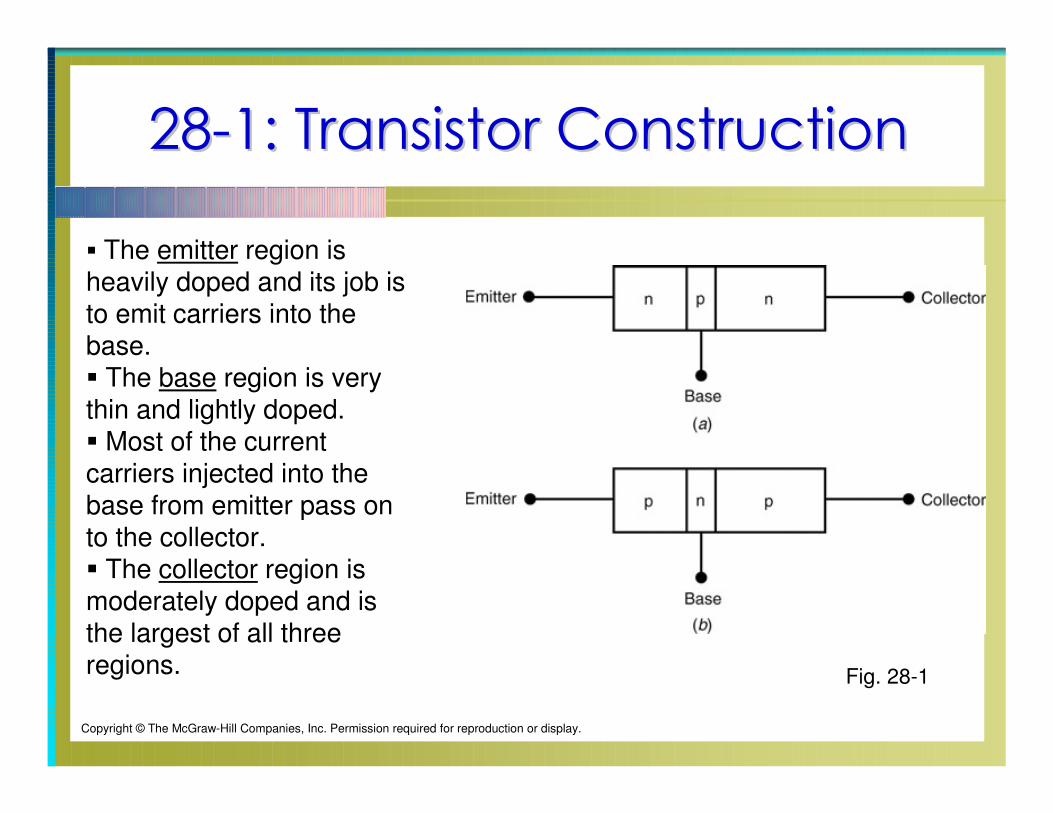
� The emitter region is heavily doped and its job is to emit carriers into the base.� The base region is very thin and lightly doped.� Most of the current carriers injected into the base from emitter pass on to the collector.� The collector region is moderately doped and is the largest of all three regions.

EB

C

Bipolar Transistors

Base

Collector

Emitter

Base

Collector

N

P

N

P

N

P

Emitter

2828--2: Proper Transistor Biasing2: Proper Transistor Biasing

� For a transistor to function properly as an amplifier, the emitter-base junction must be forward-biased and the collector-base junction must be reverse-biased.

� The common connection for the voltage sources are at the base lead of the transistor.

� The emitter-base supply voltage is designated VEE and the collector-base supply voltage is designated VCC.

� For silicon, the barrier potential for both EB and CB junctions equals 0.7 V

Schematic SymbolSchematic Symbol

Reverse

bias

Forward

bias

Transistor Biasing

IE

IC

IB

IE = IB + IC

Base

Emitter

Collector

N

P

N

2828--2: Proper Transistor Biasing2: Proper Transistor Biasing

Copyright © The McGraw-Hill Companies, Inc. Permission required for reproduction or display.

Fig. 28-4

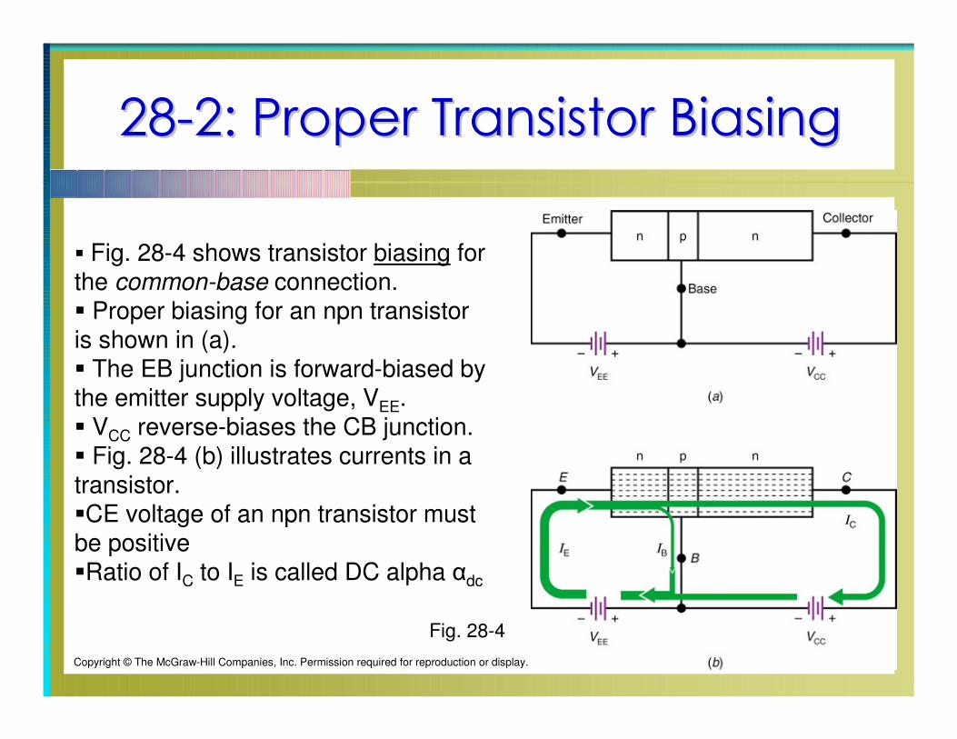
� Fig. 28-4 shows transistor biasing for the common-base connection.� Proper biasing for an npn transistor is shown in (a).� The EB junction is forward-biased by the emitter supply voltage, VEE.� VCC reverse-biases the CB junction.� Fig. 28-4 (b) illustrates currents in a transistor.�CE voltage of an npn transistor must be positive�Ratio of IC to IE is called DC alpha αdc

2828--3: Operating Regions3: Operating Regions

�Since emitter lead is common, this connection is called common-emitter connection �Collector current IC is controlled solely by the base current, IB.� By varying IB, a transistor can be made to operate in any one of the following regions

� Active

� Saturation� Breakdown� Cutoff

�Ratio of IC to IB is called DC beta βdc

Fig. 28-6: Common-emitter connection (a)

circuit. (b) Graph of IC versus VCE for different base current values.

2828--3: Operating Regions3: Operating Regions

� Active Region

� Collector curves are nearly horizontal

� IC is greater than IB (IC = βdc X IB)

� Saturation

� IC is not controlled by IB� Vertical portion of the curve near the origin

� Breakdown

� Collector-base voltage is too large and collector-base diode breaks down

� Undesired collector current

� Cutoff

� IB = 0

� Small collector current flows IC ≈ 0

Transistor CurrentsTransistor Currents

� IE = IB + IC� IC = IE – IB� IB = IE – IC

� βdc =

� αdc =

� αdc =

IC

IBIC

IE

βdc

1 + βdc

Example 28Example 28--44

� A transistor has the following currents:

IE = 15 mA

IB = 60 µA

Calculate αdc, and βdc

� IC = IE – IB = 14.94 mA

� αdc = 0.996

� βdc = 249

2828--3: Operating Regions3: Operating Regions

Copyright © The McGraw-Hill Companies, Inc. Permission required for reproduction or display.

Fig. 28-7

� Fig. 28-7 shows the dc equivalent circuit of a transistor operating in the active region.

� The base-emitter junction acts like a forward-biased diode with current, IB.

� Usually, the second approximation of a diode is used.

� If the transistor is silicon, assume that VBE equals 0.7 V.

2828--4: Transistor Ratings4: Transistor Ratings

� A transistor, like any other device, has limitations on its operations.

� These limitations are specified in the manufacturer’s data sheet.

� Maximum ratings are given for

� Collector-base voltage

� Collector-emitter voltage

� Emitter-base voltage

� Collector current

� Power dissipation

2828--5: Checking a Transistor 5: Checking a Transistor

with an Ohmmeterwith an Ohmmeter

Fig. 28-8

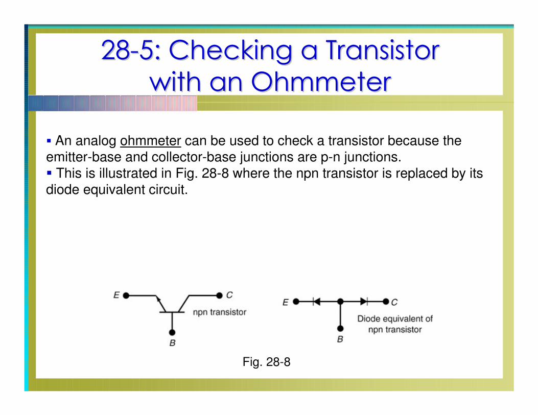
� An analog ohmmeter can be used to check a transistor because the emitter-base and collector-base junctions are p-n junctions.� This is illustrated in Fig. 28-8 where the npn transistor is replaced by its diode equivalent circuit.

Using a DMM to check a DiodeUsing a DMM to check a Diode

� Ohmmeter ranges in DMMs do not provide the proper forward bias to turn on the diode

� Set DMM to the special diode range

� In forward-bias, digital display indicates the forward voltage dropped across the diode

� In reverse-bias, digital display indicates an over range condition

� For silicon diode, using an analog meter, the ratio of reverse resistance, RR, to forward resistance, RF, should be very large such as 1000:1 or more

2828--5: Checking a Transistor 5: Checking a Transistor

with an Ohmmeterwith an Ohmmeter

Copyright © The McGraw-Hill Companies, Inc. Permission required for reproduction or display.

Fig. 28-9

� To check the base-emitter junction of an npn transistor, first connect the ohmmeter as shown in Fig. 28-9 (a) and then reverse the ohmmeter leads as shown in (b).� For a good p-n junction made of silicon, the ratio RR/RF should be equal to or greater than 1000:1.

2828--5: Checking a Transistor 5: Checking a Transistor

with an Ohmmeterwith an Ohmmeter

Copyright © The McGraw-Hill Companies, Inc. Permission required for reproduction or display.

Fig. 28-10

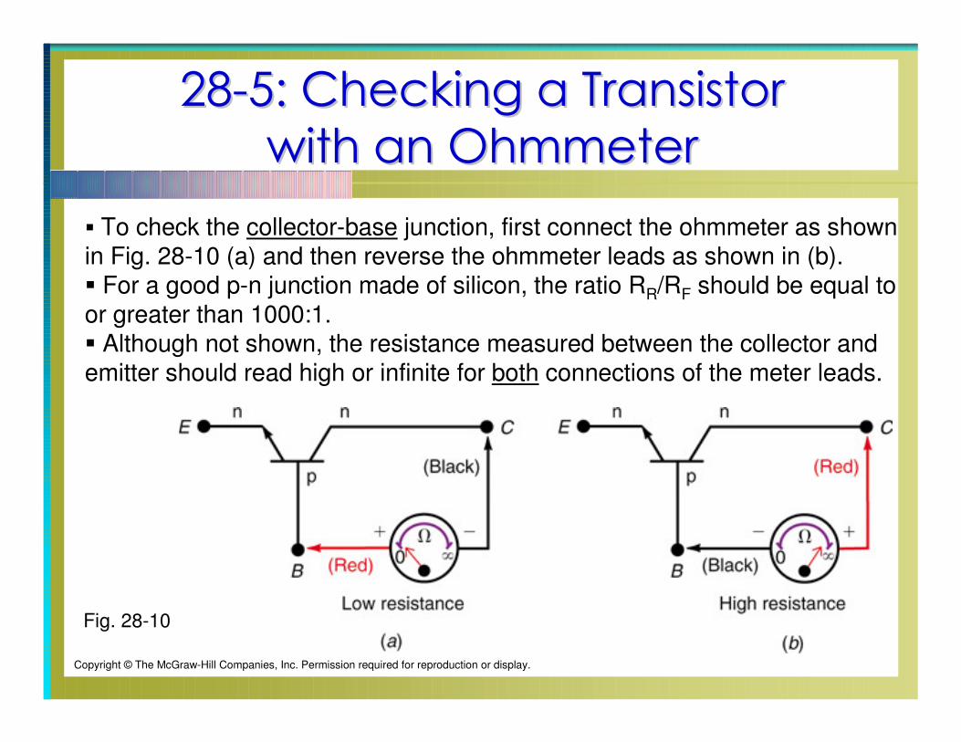
� To check the collector-base junction, first connect the ohmmeter as shown in Fig. 28-10 (a) and then reverse the ohmmeter leads as shown in (b).� For a good p-n junction made of silicon, the ratio RR/RF should be equal to or greater than 1000:1.� Although not shown, the resistance measured between the collector and emitter should read high or infinite for both connections of the meter leads.

2828--6: Transistor Biasing6: Transistor Biasing

� For a transistor to function properly as an amplifier, an external dc supply voltage must be applied to produce the desired collector current.

� Bias is defined as a control voltage or current.

� Transistors must be biased correctly to produce the desired circuit voltages and currents.

� The most common techniques used in biasing are

� Base bias

� Voltage-divider bias

� Emitter bias

2828--6: Transistor Biasing6: Transistor Biasing

Fig. 28-12

Copyright © The McGraw-Hill Companies, Inc. Permission required for reproduction or display.

� Fig. 28-12 (a) shows the simplest way

to bias a transistor, called base bias.� VBB is the base supply voltage, which is used to forward-bias the base-emitter junction.� RB is used to provide the desired

value of base current.� VCC is the collector supply voltage, which provides the reverse-bias voltage required for the collector-base junction.� The collector resistor, RC, provides

the desired voltage in the collector circuit

Transistor BiasingTransistor Biasing: Base Biasing

� A more practical way to provide base bias is to use

one power supply.

IB = VCC - VBE

RB

IC ≈ βdc x IB

VCE ≈ VCC - ICRC

2828--6: Transistor Biasing6: Transistor Biasing

Copyright © The McGraw-Hill Companies, Inc. Permission required for reproduction or display.

Fig. 28-14

� The dc load line is a graph that allows us to determine all possible combinations of IC and VCE for a given amplifier.

� For every value of collector current, IC, the corresponding value of VCE can be found by examining the dc load line.

� A sample dc load line is shown in Fig. 28-14.

2828--6: Transistor Biasing6: Transistor BiasingMidpoint BiasMidpoint Bias

� Without an ac signal applied to a transistor, specific values ofIC and VCE exist at a specific point on a dc load line

� This specific point is called the Q point (quiescent currents and voltages with no ac input signal)

� An amplifier is biased such that the Q point is near the center of dc load line

� ICQ = ½ IC(sat)

� VCEQ = ½ VCC

� Base bias provides a very unstable Q point, because IC and VCE are greatly affected by any change in the transistor’s beta value

2828--6: Transistor Biasing6: Transistor Biasing

Copyright © The McGraw-Hill Companies, Inc. Permission required for reproduction or display.

Fig. 28-15

Fig. 28-15 illustrates a dc load lineshowing the end points IC (sat) and VCE (off), as well as the Q point values ICQ and VCEQ.

Base Bias Base Bias –– Example 1Example 1

� Solve for IB, IC and VCE

� Construct a dc load line showing the values of IC(sat), VCE(off), ICQ and VCEQ

Base Bias Base Bias –– Example 2Example 2

� Solve for IB, IC and VCE

� Construct a dc load line showing the values of IC(sat), VCE(off), ICQ and VCEQ

2828--6: Transistor Biasing6: Transistor Biasing

Copyright © The McGraw-Hill Companies, Inc. Permission required for reproduction or display.

Fig. 28-18

� The most popular way to bias a transistor is with voltage-divider bias.

� The advantage of voltage-divider bias lies in its stability.

� An example of voltage-divider bias is shown in Fig. 28-18.

VB = X VCC

R2

R1 + R2

VE = VB - VBE

IE ≈ IC

Voltage Divider Bias Voltage Divider Bias –– ExampleExample

� Solve for VB, VE, IE, IC, VC and VCE

� Construct a dc load line showing the values of IC(sat), VCE(off), ICQ and VCEQ

2828--6: Transistor Biasing6: Transistor Biasing

Copyright © The McGraw-Hill Companies, Inc. Permission required for reproduction or display.

Fig. 28-19

� Fig. 28-19 shows the dc load line for voltage-divider biased transistor circuit in Fig. 28-18.� End points and Q points are

�IC (sat) = 12.09 mA�VCE (off) = 15 V� ICQ = 7 mA� VCEQ = 6.32 V

2828--6: Transistor Biasing6: Transistor Biasing

Copyright © The McGraw-Hill Companies, Inc. Permission required for reproduction or display.

Fig. 28-23

� Both positive and negative power supplies are available

�Emitter bias provides a solid Q point that fluctuates very little with temperature variation and transistor replacement.

Emitter Bias Emitter Bias –– ExampleExample

� Solve for IE, and VC


Recommended