PAPERS A MOSFETPowerAmplifier with Error Correction* ROBERT R. CORDELL Regional Bell Operating Companies, Central Services Organization, Holmdel, NJ 07733, USA Power MOSFETs are emerging as the device of choice for high-quality power amplifiers because of their speed, reduced need for protection, and falling cost. A low-distortion power amplifier design is presented which includes output stage error correction to reduce the effect of transconductance droop in the crossover region and thus allow operation at more efficient bias levels. 0 INTRODUCTION In this paper we present a high-performance amplifier The rapid evolution of power MOSFETs during the design which utilizes the advantages of the power last few years has brought them to the point where they MOSFET while dealing with the drawbacks of the de- are now very attractive for use in audio amplifier power vice. Although not taken to an extreme, the underlying output stages. Important improvements include in- philosophy of the design is that small-signal silicon is creased voltage, current, and dissipation ratings, re- inexpensive, that is, that the overwhelming portion of duced "on" resistance, availability of complementary expense in a power amplifier is in items like the power pairs, and greatly reduced cost. Although a 75-W transformer, filter capacitors, power transistors, heat sinks, chassis, and related hardware. Thus, in order to MOSFET is still more expensive than a 150-W bipolar transistor, the premium is small when considered rel- take full advantage of the performance achievable with ative to total amplifier cost and improved performance, the MOSFET output stage, a very-high-quality front The purpose of this paper is to demonstrate the level end and driver are provided. The driver, operating from of performance achievable with current technology and regulated boosted supplies, is capable of providing high to illustrate practical circuit techniques for achieving voltage and current swings to the power MOSFETs this performance, with good headroom. Output stage transconductance Power MOSFETs have several fundamental advan- droop is dealt with by employing a simple but very effective output stage error-correction technique pro- rages over bipolar power transistors, most notably speed and freedom from secondary breakdown. The latter posed by Hawksford [ 1]. The resulting design achieves provides higher "usable" power dissipation, improved a 20-kHz total harmonic distortion figure of less than reliability, and freedom from safe-area limiter circuits, 0.0015% at an idle bias of only 150 mA. which can misbehave and cause audible degradation. I APPLYING POWER MOSFETS MOSFETs also have some disadvantages in comparison with bipolar transistors. These include higher turn-on The design of MOSFET power amplifiers is quite voltage drive requirements and smaller transconduct- straightforward and conventional as long as differences ance at low current levels. The former tends to contradict between MOSFETs and bipolar transistors are under- generalizations that have been made to the effect that stood. In this section we review current MOSFET drive circuits for power MOSFETs are less expensive, technology, compare MOSFET and bipolar character- at least for the reliable source-follower configuration, istics, and focus on several important design consid- The latter results in transconductance droop in the cross- erations. over region if bias currents are not fairly high. Such transconductance droop can result in crossover distortion. 1.1 Power MOSFETStructures Power FET technology has evolved over the last 15 * Presented at the 72nd Convention of the Audio Engi- neering Society, Anaheim, CA, 1982 October 23-27; revised years from JFET to MOSFET devices with many dil- l983 July 25 and October 27. ferent structures along the way. The modern power 2 J. Audio Eng.Soc., Vol.32, No.1/2, 1984January/February
Transcript
PAPERS
A MOSFETPowerAmplifier with ErrorCorrection*
ROBERT R. CORDELL
Regional Bell Operating Companies, Central Services Organization, Holmdel, NJ 07733, USA
Power MOSFETs are emerging as the device of choice for high-quality power amplifiers
because of their speed, reduced need for protection, and falling cost. A low-distortion
power amplifier design is presented which includes output stage error correction to
reduce the effect of transconductance droop in the crossover region and thus allowoperation at more efficient bias levels.
0 INTRODUCTION In this paper we present a high-performance amplifier
The rapid evolution of power MOSFETs during the design which utilizes the advantages of the powerlast few years has brought them to the point where they MOSFET while dealing with the drawbacks of the de-are now very attractive for use in audio amplifier power vice. Although not taken to an extreme, the underlyingoutput stages. Important improvements include in- philosophy of the design is that small-signal silicon iscreased voltage, current, and dissipation ratings, re- inexpensive, that is, that the overwhelming portion ofduced "on" resistance, availability of complementary expense in a power amplifier is in items like the powerpairs, and greatly reduced cost. Although a 75-W transformer, filter capacitors, power transistors, heat
sinks, chassis, and related hardware. Thus, in order toMOSFET is still more expensive than a 150-W bipolartransistor, the premium is small when considered rel- take full advantage of the performance achievable withative to total amplifier cost and improved performance, the MOSFET output stage, a very-high-quality front
The purpose of this paper is to demonstrate the level end and driver are provided. The driver, operating fromof performance achievable with current technology and regulated boosted supplies, is capable of providing highto illustrate practical circuit techniques for achieving voltage and current swings to the power MOSFETsthis performance, with good headroom. Output stage transconductance
Power MOSFETs have several fundamental advan- droop is dealt with by employing a simple but veryeffective output stage error-correction technique pro-
rages over bipolar power transistors, most notably speedand freedom from secondary breakdown. The latter posed by Hawksford [1]. The resulting design achieves
provides higher "usable" power dissipation, improved a 20-kHz total harmonic distortion figure of less thanreliability, and freedom from safe-area limiter circuits, 0.0015% at an idle bias of only 150 mA.
which can misbehave and cause audible degradation. I APPLYING POWER MOSFETSMOSFETs also have some disadvantages in comparison
with bipolar transistors. These include higher turn-on The design of MOSFET power amplifiers is quitevoltage drive requirements and smaller transconduct- straightforward and conventional as long as differencesance at low current levels. The former tends to contradict between MOSFETs and bipolar transistors are under-generalizations that have been made to the effect that stood. In this section we review current MOSFET
drive circuits for power MOSFETs are less expensive, technology, compare MOSFET and bipolar character-at least for the reliable source-follower configuration, istics, and focus on several important design consid-The latter results in transconductance droop in the cross- erations.over region if bias currents are not fairly high. Suchtransconductance droop can result in crossover distortion. 1.1 Power MOSFETStructures
Power FET technology has evolved over the last 15* Presented at the 72nd Convention of the Audio Engi-neering Society, Anaheim, CA, 1982 October 23-27; revised years from JFET to MOSFET devices with many dil-l983 July 25 andOctober 27. ferent structures along the way. The modern power
PAPERS MOSFET POWER AMPLIFIER WITH ERRORCORRECTION
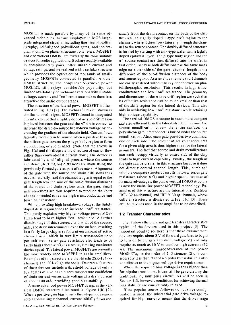
MOSFET is made possible by many of the same ad- tically from the drain contact on the back of the chipvanced techniques that are employed in MOS large- through the lightly doped n-type drift region to thescale integrated circuits, including fine-line photolith- channel, where it then flows laterally through the chan-ography, self-aligned polysilicon gates, and ion im- nel to the source contact. The doubly diffused structureplantation. Two planar structures, one lateral MOSFET is formed by starting with an n-type wafer with a lightlyand one vertical DMOS, are currently the most suitable doped epitaxial layer. The p-type body region and thedevices foraudio applications. Both are readily available n+ source contact are then diffused into the wafer inin complementary pairs, offer suitable current and that order. Because both diffusions use the same maskvoltage ratings, and are realized with a cellular structure edge on either side of the gate, channel length is thewhich provides the equivalent of thousands of small- difference of the out-diffusion distances of the body'geometry MOSFETs connected in parallel. Another and source regions. As a result, extremely short channelsDMOS structure, the nonplanar V-groove power are easily realized without heavy dependence on pho-MOSFET, still enjoys considerable popularity, but tolithographic resolution. This results in high trans-limited availability ofp-channel versions with suitable conductance and low "on" resistance. The geometryvoltage, current, and "on" resistance makes them less and dimensions of the n-type drift region are such that
· attractive for audio output stages, its effective resistance can be much smaller than thatThe structure of the lateral power MOSFET is illus- of the .drift region for the lateral devices. This also
trated in Fig. l(a) [2]. The n-channel device shown is aids in achieving low "on" resistance while retainingsimilar to small-signal MOSFETs found in integrated high voltage capability.circuits, except that a lightly doped n-type drift region The vertical DMOS structure is much more compactis placed between the gate and the n + drain contact to and area-efficient than the lateral structure because theincrease the drain-to-source breakdown voltage by de- source metallization covers the entire surface; thecreasing the gradient of the electric field. Current flows polysilicon gate interconnect is buried under the sourcelaterally from drain to source when a positive bias on metallization. Also, each gate provides two channels,the silicon gate inverts the p-type body region to form one on each side. The amount of active channel areaa conducting n-type channel. (Note that the arrows in for a given chip area is thus higher than for the lateralFig. l(a) and (b) illustrate the direction of carrier flow geometry. The fact that source and drain metallizationsrather than conventional current flow.) The device is can each occupy virtually an entire side of the chip
fabricated by a self-aligned process where the source leads to high current capability. Finally, the length ofand drain (drift region) diffusions are made using the the gate can be greater in this structure because it doespreviously formed gate as part of the mask. Alignment not directly control channel length. This, combinedof the gate with the source and drain diffusions thus with the compact structure, results in lower series gateoccurs naturally, and the channel length is equal to the resistance (about 6 fl) and higher speed. Because ofgate length less the sum of the out-diffusion distances its many advantages, the planar vertical DMOS structureof the source and drain regions under the gate. Small is now the main-line power MOSFET technology. Ex-gate structures are thus required to produce the short amples of this structure are the International Rectifierchannels needed to realize high transconductance and IRF-132 (n-channel) and IRF-9130 (p-channel), whoselow "on" resistance, cellular structure is illustrated in Fig. l(c) [3]. These
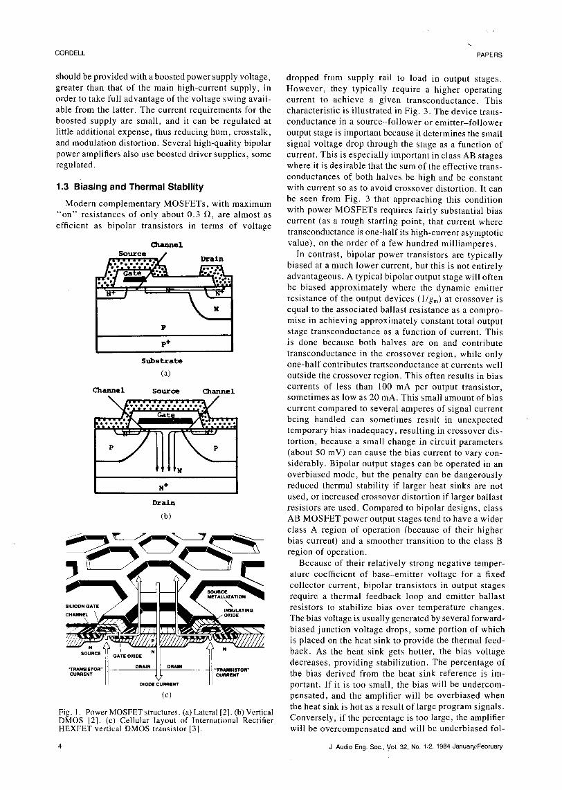
While providing high breakdown voltage, the lightly are the devices used in the amplifier to be described.doped drift region tends to increase "on" resistance.This partly explains why higher voltage power MOS- 1.2 Transfer CharacteristicsFETs tend to have higher "on" resistance. A furtherdisadvantage of this structure is that all of the source, Fig. 2 shows the drain and gate transfer characteristics
gate, and drain interconnect lies on the surface, resulting typical of the devices used in this project [3]. Thein a fairly large chip area for a given amount of active important point to see here is that these enhancementchannel area, which in turn limits transconductance devices require about 3 V of forward gate bias to begin
per unit area. Series gate resistance also tends to be to turn on (e.g., gate threshold voltage Vt) and mayfairly high (about 40 12) as a result, limiting maximum require as much as 10 V to conduct high currents (12device speed. The lateral power MOSFETs are presently A). The maximum transconductance of the powerthe most widely used MOSFET in audio amplifiers. MOSFETs, on the order of 2-5 siemens (S), is con-
Examples of this structure are the Hitachi 2SK-134 (n- siderably less than that of a bipolar transistor; this alsochannel) and 2SJ-49 (p-channel). Desirable features contributes to the higher voltage drive requirement.of these devices include a threshold voltage of only a While the required bias voltage is thus higher thanfew tenths of a volt and a zero temperature coefficient for bipolar transistors, it can still be generated by theof drain current versus gate voltage at a drain current traditional Vbe multiplier circuit. As will be seen inof about 100 mA, providing good bias stability. Section 1.3, however, conditions for achieving thermal
A more advanced power MOSFET design is the ver- bias stability are considerably relaxed.tical DMOS structure illustrated in Figure l(b) [2]. If the popular source-follower output stage config-
When a positive gate bias inverts the p-type body region uration is used, the substantial gate drive voltage re-into a conducting n channel, current initially flows ver- quired for high currents means that the driver stage
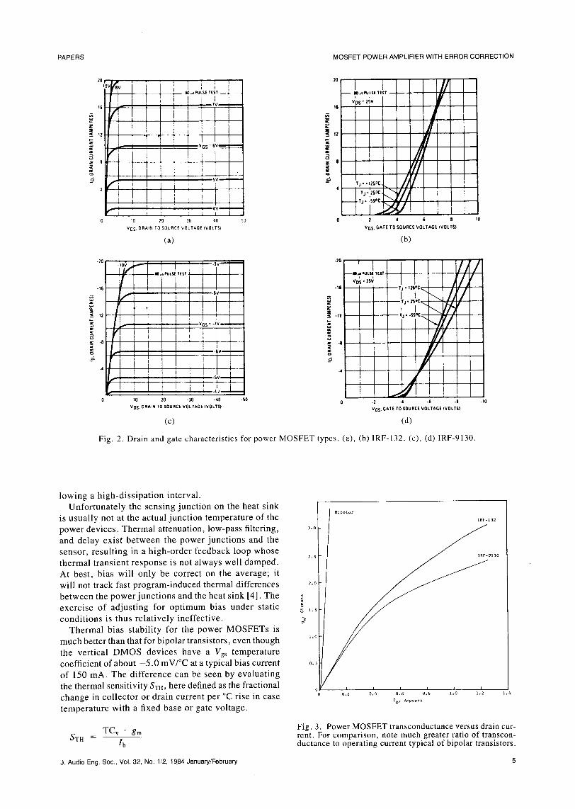
should be provided with a boosted power supply voltage, dropped from supply rail to load in output stages.greater than that of the main high-current supply, in However, they typically require a higher operatingorder to take full advantage of the voltage swing avail- current to achieve a given transconductance. Thisable from the latter. The current requirements for the characteristic is illustrated in Fig. 3. The device trans-boosted supply are small, and it can be regulated at conductance in a source-follower or emitter-followerlittle additional expense, thus reducing hum, crosstalk, output stage is important because it determines the small
and modulation distortion. Several high-quality bipolar signal voltage drop through the stage as a function ofpower amplifiers also use boosted driver supplies, some current. This is especially important in class AB stagesregulated, whereit is desirablethatthe sumof theeffective trans-
conductances of both halves be high and be constant1.3 Biasing and Thermal Stability with current so as to avoid crossover distortion. It can
be seen from Fig. 3 that approaching this conditionModern complementary MOSFETs, with maximumwith power MOSFETs requires fairly substantial bias"on" resistances of only about 0.3 _, are almost as
efficient as bipolar transistors in terms of voltage current (as a rough starting point, that current wheretransconductance is one-half its high-current asymptotic
nam-reel value), on the order of a few hundred milliamperes.
Source D_ain In contrast, bipolar power transistors are typicallybiased at a much lower current, but this is not entirelyadvantageous. A typical bipolar output stage will oftenbe biased approximately where the dynamic emitterresistance of the output devices (1/gm) at crossover isequal to the associated ballast resistance as a compro-mise in achieving approximately constant total output
P stage transconductance as a function of current. Thisp+ is done because both halves are on and contribute
transconductance in the crossover region, while onlysubst, rate one-half contributes transconductance at currents well
(a) outside the crossover region. This often results in biascurrents of less than 100 mA per output transistor,Channel Sourc_ Channelsometimes as low as 20 mA. This small amount of bias
current compared to several amperes of signal currentbeing handled can sometimes result in unexpectedtemporary bias inadequacy, resulting in crossover dis-
tortion, because a small change in circuit parameterst, P (about 50 reV) can cause the bias current to vary con-
siderably. Bipolar output stages can be operated in an
N overbiased mode, but the penalty can be dangerouslyN+ reduced thermal stability if larger heat sinks are not
used, or increased crossover distortion if larger ballastDrain resistors are used. Compared to bipolar designs, class
(b) AB MOSFETpower output stages tend to have a widerclass A region of operation (because of their higherbias current) and a smoother transition to the class Bregion of operation.
Becauseof theirrelativelystrongnegativetemper-ature coefficient of base-emitter voltage for a fixed
collector current, bipolar transistors in output stagesrequire a thermal feedback loop and emitter ballast
sIuco,aAT[ m,u_,ING resistors to stabilize bias over temperature changes.C.*.._L ,ox,_ The bias voltage is usually generated by several forward-
biased junction voltage drops, some portion of whichis placed on the heat sink to provide the thermal feed-
SOURC_G*TEOX,D_ back. As the heat sink gets hotter, the bias voltagedecreases, providing stabilization. The percentage of
"TRANSISTOR" DRAIN DRAIN "TRhlNt$llrrOR"
C"""ENT CURRENT the bias derived from the heat sink reference is im-
DIDOECURRE._ portant. If it is too small, the bias will be undercom-
(c) pensated, and the amplifier will be overbiased whenthe heat sink is hot as a result of large program signals.
Fig. 1. Power MOSFET structures. (a) Lateral [2]. (b) VerticalDMOS [2]. (c) Cellular layout of International Rectifier Conversely, if the percentage is too large, the amplifierHEXFET vertical DMOS transistor [31. will be overcompensated and will be underbiased fol-
ii t'_ : !, i T"s"_7i, , i _ ', , ,v l10 20 _0 40 _'0 2 4 6 It 10
VG$ ' DRAIN T0 SOURCE VOLTAGE tVGLT$1 VGS, GATE TO SOURCE VOLTAGE IVnLTS)
(a) (b)
I tt_o , I I ,,, -,0i i //'/fl ,0;.,,_ t'l,/
" ,_! ,v "' 't'"T'_./;7._ i , ! ?.,,?_-"[ i I ,.,_" I -( ""ss"-._ _t
.-"Jill i ] e: ///'.-_" ' I loIt- r/o , I , sv j
' 1_ I/_ , i i °-4 e- I ! [ '4 I ,, _ s,, I I _t r
0 10 20 40 -40 -50 -2 -4 -8 -8 -10
VO$. DRAIN TO SOURCE VOLTAGE (VOLTS) VGS , GATE TO.SOURCE VOLTAGE (VOLTS)
(c) (d)
Fig. 2. Drain and gate characteristics for power MOSFET types. (a), (b) IRF-132. (c), (d) IRF-9130.
lowing a high-dissipation interval.Unfortunately the sensing junction on the heat sink
is usually not at the actual junction temperature of the "_"°"_ _.__._power devices. Thermal attenuation, low-pass filtering, _.oand delay exist between the power junctions and the
sensor, resulting in a high-orderfeedbackloop whose ...........thermal transient response is not always well damped.At best, bias will only be correct on the average; it
will not track fast program-induced thermal differences , _.0between the power junctions and the heat sink [4]. The
exercise of adjusting for optimum bias under static _ ,._conditions is thus relatively ineffective.Thermal bias stability for the power MOSFETs is
much better than that for bipolar transistors, even though _.o
the vertical DMOS devices have a Vgs temperaturecoefficient of about -5.0 mV/°C at a typical bias current o._of 150 mA. The difference can be seen by evaluating
the thermal sensitivity Sm, here defined as the fractional 0 I I
0.8 1,0 l.t*
change in collector or drain current per °C rise in case ..... _ 0_ _.'_ID, Amperes
temperature with a fixed base or gate voltage.
Fig. 3. Power MOSFET transconductance versus drain cur-TCv · gm rent. For comparison, note much greater ratio of transcon-
STH -- lb ductance to operating current typical of bipolar transistors.
where TCv is the base or gate voltage temperature coef- at a specified gate voltage is important. Specifically,ficient for constant collector or drain current, gm is the recognizing that the gate threshold voltage specificationstage transconductance (including the effect of emitter for thesedevices is 2-4 V, an examination of the gate
ballast resistors if present), and lb is the nominal bias transfer characteristics of Fig. 2 indicates'that a very
current. For a bipolar design- biased at 80 mA with serious current imbalance can exist unless gate threshold ..0.33-llemitter-.resistors, STH = 0.0427°C. For aMOS- voltages among'paralleled devices are reasonablyFET stage biased at 150 mA with no source resistors matched. It is also'apparent that reasonable temperatureand a device transconductance.of 0.5 S, STH = 0.017/ differentials will not adequately reduce the imbalance.
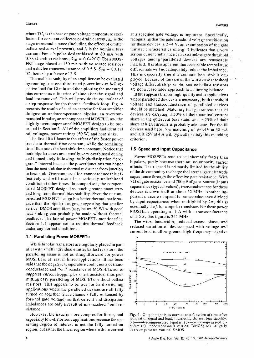
°C,-better by a factor of 2.5. This is especially true if a common heat-sink is em:Thermal bias stability of an amplifier can be evaluated ployed. Because of the size of the worst Case th?esfiold '_' '
.by running it at one-third rated power into an 8-1_ re- voltage differentials possible, source ballast'resistorssistive load for 10 min and .then:plotting the measured are not a reasonable approach to achieving 'balance_bias current as a function of time. after the signal and It thus appears thatfor high-quality audio applications "load are removed· This will provide the ,equivalent of where paralleled devices are necessary, both thresholda step response for the thermal feedback loop. Fig. 4 voltage and transconductance of paralleled:devicespresents the results of such an exercise for four amplifier should be matched. Matching that guarantees that a'lldesigns: an undercompensated' bipolar, an overcom- devices are carrying _+50% of their nominal'cfirrentpensated bipolar, an uncompensated MOSFET, and the share in the quiescent bias state, and _+25% of their
slightly overcompensated MOSFET design to be pre- share at high currents is probably adequate. For the IRsented in Section 2. All of the amplifiers had identical devices used here, VGs matching of +0.-1V at 50 mA
rail voltages, power ratings (50 W) and heat sinks, and + 0.25V at 4 A will typically satisfy this matchingThe first 10 s illustrate the effect of the faster power criterion.
transistor thermal time constant, while the remainingtime illustrates the heat sink time constant. Notice that 1.5 Speed and Input Capacitance
both bipolar cases are actually very overbiased during Power MOSFETs tend to be inherently faster thanand immediatelyfollowingthe high-dissipation"pro-gram" interval because the power junctions run hotter bipolars, partly because there are no minority carrier
than the heat sink due to thermal resistance from junction effects. Their speed is primarily limited by the abilityto heat sink. Overcompensation cannot reduce this ef- of the drive circuitry to charge the internal gate electrodefectively and will result in a seriously underbiased capacitance through the effective gate resistance. With
7 _ of gate resistance and 700 pF of gate-source (input)condition at other times. In comparison, the compen-capacitance (tyFical values), transconductance for these
sated MOSFET design has much greater short-term devices is down 3 dB at about 32 MHz. Another im-and long-term thermal bias stability. Even the uncom-pensated MOSFET'design has better thermal perform- portant measure of speed is transconductance dividedance than the bipolar designs, suggesting that smaller by input capacitance; when multiplied by 2_, this is
essentially theft for a bipolar transistor. For these powervertical DMOS amplifiers (say, below 50 W) with good MOSFETs operating at 1 A with a transconductanceheat sinking can probably be made without thermal
of 1.5 S, this figure is 341 MHz.feedback. The lateral power MOSFETs mentioned inThe wider bandwidth, reduced excess phase, andSection 1.1 appear not to require thermal feedback
under any normal conditions, reduced variation of device speed with voltage andcurrent tend to allow greater high-frequency negative
1.4 Paralleling Power MOSFETsI I I I I IIII I I I I I IIII I I I I [ I I I
While bipolar transistors are regularly placed in par-allel with small individual emitter ballast resistors, the SOB
BIAS CURRENT vs. TIME
paralleling issue is not as straightforward for power
MOSFETs, at least in linear applications. It has been _ _c_said that the negative temperature coefficients of trans- 200__ c._
conductance and "on" resistance of MOSFETs act to _ 10o_-'"""'"'"---4_-_suppress current hogging by one transistor, thus per-
mitting easy paralleling of MOSFETs without ballast _ ,o _(b_resistors. This appears to be true for hard-switchingapplications where the paralleled devices are all fullyturned on together (i.e., channels fully enhanced by 20
forward gate voltage) so that current and dissipation io .................... . ....imbalancesare only a result of mismatched "on" re......................sistance. ,IRE,S,co._
However, the issue is more complex for linear, and Fig. 4. Output stage bias current as a function of time after
especially low-distortion, applications because the op- removal of signal and load, illustrating thermal bias stability.(a)--undercompensated bipolar; (b)--overcompensated bi-
erating region of interest is not the fully turned on polar; (c)--uncompensated vertical DMOS; (d)--slightlyregion, but rather the linear region wherein drain current overcompensated vertical DMOS.
feedback with greater stability. The higher switching up to a region where they are more easily damped byspeed also tends to reduce dynamic crossover distortion, introducing a reasonable amount of loss. Such loss isThe MOSFET's higher switching speed also greatly most often introduced with a small resistor (typicallyreduces the flow of class AB common-mode current at 50-500 f_) in series with the gate of each power MOS-high frequencies, which poses such a destructive threat FET. Unfortunately this resistor, in combination withto many bipolar designs, the gate-source capacitance, degrades the speed of the
Although power MOSFETs require virtually no drive power MOSFET. The challenge is to eliminate the par-current at low frequencies, their substantial input ca- asitic oscillations without giving up too much speed.pacitance means that drive circuits with forward and Ferrite beads in the gate or drain leads can also bereverse drive capabilities similar to those employed for effective.bipolar output stages should be used for wideband high- Paralleling of power MOSFETs can increase theslew-rate circuits in demanding audio applications, tendency to parasitic oscillation because more activeAlthough the gate-source capacitance can be on the and reactive elements are being added to the system,order of 700 pF, this capacitance is effectively "boot- increasing the opportunities for formation of an efficientstrapped" in a source-follower output stage, typically oscillator [5]. The techniques for avoiding oscillationsreducing its effect by about an order of magnitude. The in this situation are, however, the same as for the non-
smaller gate-drain capacitance, about 100 pF, is also paralleled case. Loss elements are applied individuallypresent. A 100-V/txs slope with an effective capacitance to each power MOSFET.of 170 pF thus requires a 17-mA current capability Parasitic oscillations do not merely create distortionfrom each driver, and radio-frequency interference. They are one of the
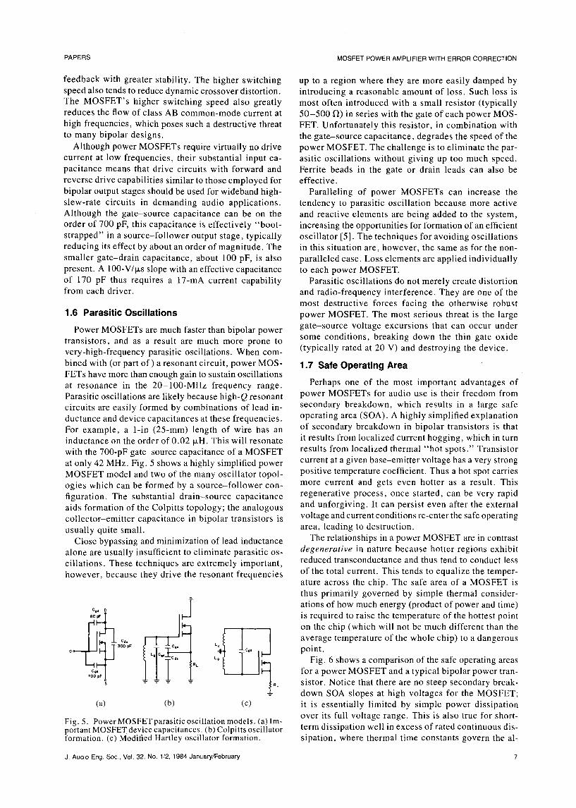
most destructive forces facing the otherwise robust1.6 Parasitic Oscillations power MOSFET. The most serious threat is the large
gate-source voltage excursions that can occur underPower MOSFETs are much faster than bipolar powertransistors, and as a result are much more prone to some conditions, breaking down the thin gate oxidevery-high-frequency parasitic oscillations. When com- (typically rated at 20 V) and destroying the device.
bined with (or part of) a resonant circuit, power MOS- 1.7 Safe Operating AreaFETs have more than enough gain to sustain oscillationsat resonance in the 20-100-MHz frequency range. Perhaps one of the most important advantages ofParasitic oscillations are likely because high-Q resonant power MOSFETs for audio use is their freedom fromcircuits are easily formed by combinations of lead in- secondary breakdown, which results in a large safeductance and device capacitances at these frequencies, operating area (SEA). A highly simplified explanationFor example, a 1-in (25-mm) length of wire has an of secondary breakdown in bipolar transistors is thatinductance on the order of 0.02 _xH. This will resonate it results from localized current hogging, which in turnwith the 700-pF gate-source capacitance of a MOSFET results from localized thermal "hot spots." Transistorat only 42 MHz. Fig. 5 shows a highly simplified power current at a given base-emitter voltage has a very strongMOSFET model and two of the many oscillator topol- positive temperature coefficient. Thus a hot spot carriesogies which can be formed by a source-follower con- more current and gets even hotter as a result. Thisfiguration. The substantial drain-source capacitance regenerative process, once started, can be very rapidaids formation of the Colpitts topology; the analogous and unforgiving. It can persist even after the externalcollector-emitter capacitance in bipolar transistors is voltage and current conditions re-enter the safe operating
usually quitesmall, area, leadingto destruction.Close bypassing and minimization of lead inductance The relationships in a power MOSFET are in contrast
alone are usually insufficient to eliminate parasitic os- degenerative in nature because hotter regions exhibitcillations. These techniques are extremely important, reduced transconductance and thus tend to conduct lesshowever, because they drive the resonant frequencies of the total current. This tends to equalize the temper-
ature across the chip. The safe area of a MOSFET isthus primarily governed by simple thermal consider-
j ations of how much energy (product of power and time)cgd
8o,_ Li__ ,f i is required to raise the temperature of the hottest point
_! onthechip(whichwillnot be muchdifferentthanthe
1 averagetemperatureof the wholechip)to a dangerous
j 30oc".F c L_ c,, point.
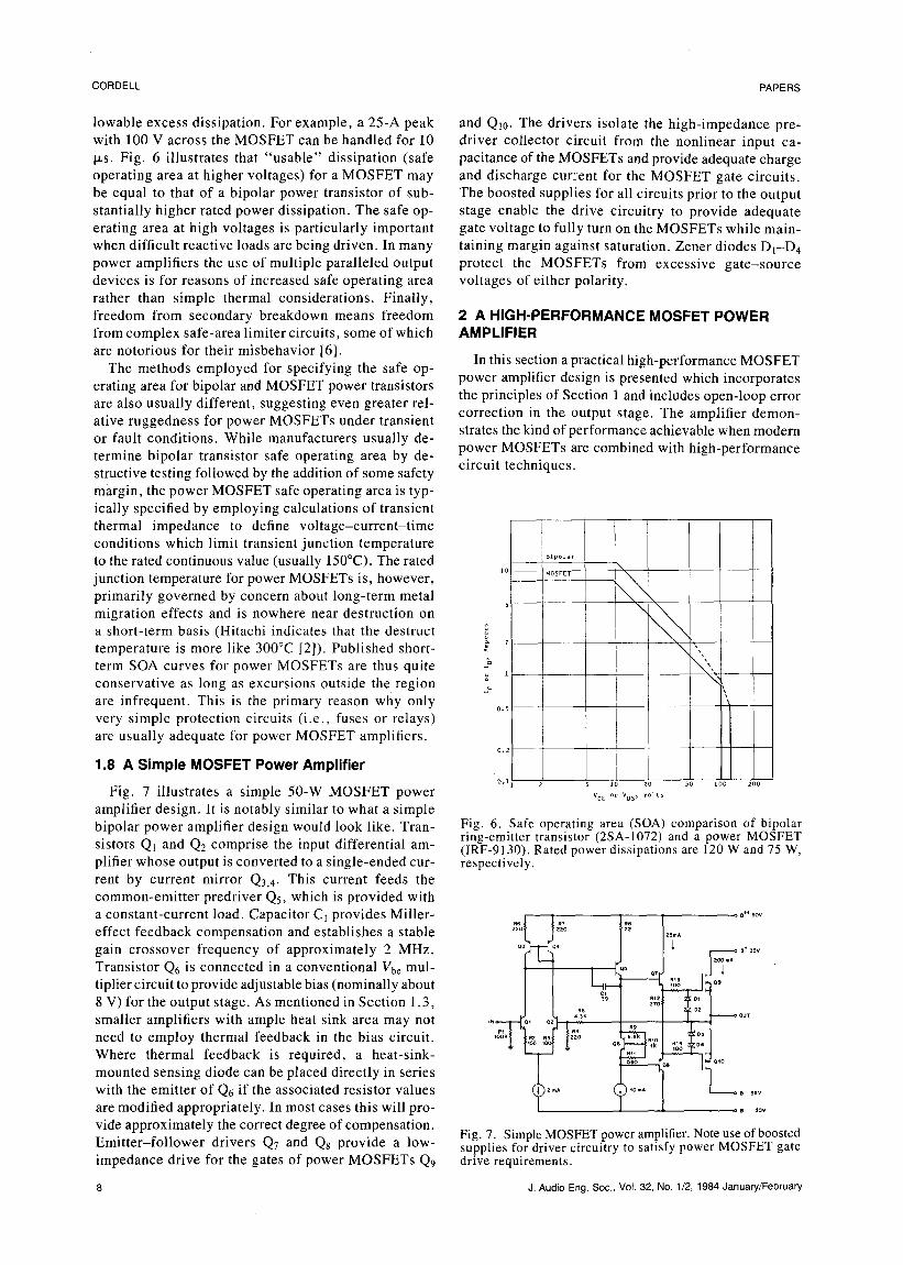
,L L'I I I_ Fig. Oshows a comparison 0f the safe operating areas
_,, for apowerMOSFETanda typicalbipolarpowertran-700 pF
.... _L sister. Notice that there are no steep secondary break-down SeA slopes at high voltages for the MOSFET;
(a) (b) (c) it is essentiallylimitedby simplepower dissipationover its full voltage range. This is also true for short-
Fig. 5. PowerMOSFETparasitic oscillation models. (a) Im-portant MOSFET device capacitances. (b) Colpitts oscillator term dissipation well in excess of rated continuous dis-formation. (c) Modified Hartley oscillator formation, sipation, where thermal time constants govern the al-
lowable excess dissipation. For example, a 25-A peak and Q10. The drivers isolate the high-impedance pre-with 100 V across the MOSFET can be handled for 10 driver collector circuit from the nonlinear input ca-lls. Fig. 6 illustrates that "usable" dissipation (safe pacitance of the MOSFETs and provide adequate chargeoperating area at higher voltages) for a MOSFET may and discharge cur=ent for the MOSFET gate circuits.be equal to that of a bipolar power transistor of sub- The boosted supplies for all circuits prior to the outputstantially higher rated power dissipation. The safe op- stage enable the drive circuitry to provide adequateerating area at high voltages is particularly important gate voltage to fully turn on the MOSFETs while main-
when difficult reactive loads are being driven. In many taining margin against saturation. Zener diodes D1-D 4power amplifiers the use of multiple paralleled output protect the MOSFETs from excessive gate-sourcedevices is for reasons of increased safe operating area voltages of either polarity.rather than simple thermal considerations. Finally,freedom from secondary breakdown means freedom 2 A HIGH-PERFORMANCE MOSFET POWERfrom complex safe-area limiter circuits, some of which AMPLIFIER
are notorious for their misbehavior [6]. In this section a practical high-performance MOSFETThe methods employed for specifying the safe op-erating area for bipolar and MOSFET power transistors power amplifier design is presented which incorporatesare also usually different, suggesting even greater rel- the principles of Section 1 and includes open-loop error
correction in the output stage. The amplifier demon-ative ruggedness for power MOSFETs under transientstrates the kind of performance achievable when modern
or fault conditions. While manufacturers usually de-termine bipolar transistor safe operating area by de- power MOSFETs are combined with high-performancestructive testing followed by the addition of some safety circuit techniques.margin, the power MOSFET safe operating area is typ-ically specified by employing calculations of transient
thermal impedance to define voltage-current-time [conditions which limit transient junction temperature rto the rated continuous value (usually 150°C). The rated .......
J 0 -- !lN_
junction temperature for power MOSFETs is, however, _m'_ ,,_
primarily governed by concern about long-termmetal xN_ N Imigration effects and is nowhere near destruction on '_
a short-termbasis (Hitachiindicatesthat the destruct i [ __temperature is more like 300°C[2]). Published short- _ x -,_,,
term SOA curves for power MOSFETsare thus quite _ '-,_,,.
conservative as long as excursionsoutside the region _ --x_t\are infrequent. This is the primary reason why only 0, ,very simple protection circuits (i.e., fuses or relays)are usually adequate for power MOSFET amplifiers.
0,2
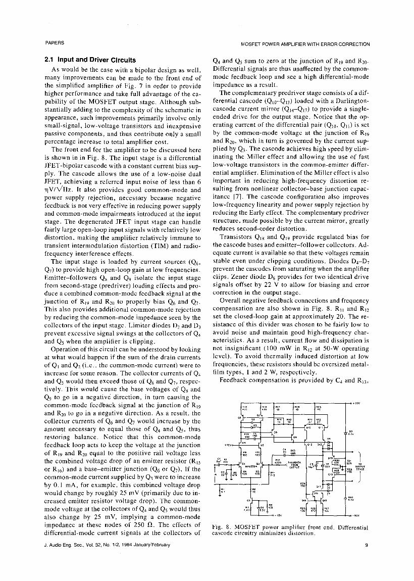
1.8 A Simple MOSFET Power Amplifier0o1 l0 20 50 100 200
Fig. 7 illustrates a simple 50-W MOSFET power *c_orvDs,.....amplifier design. It is notably similar to what a simplebipolar power amplifier design would look like. Tran- Fig. 6. Safe operating area (SOA) comparison of bipolar
ring-emitter transistor (2SA-1072) and a power MOSFETsistors Ql and Q2 comprise the input differential am- (1RF-9130). Rated power dissipations are 120 W and 75 W,plifier whose output is converted to a single-ended cur- respectively.rent by current mirror Q3,4- This current feeds thecommon-emitter predriver Q5, which is provided with
a constant-current load. CapacitorC1provides Miller- ...... _.-,oveffect feedback compensation and establishes a stable ........ 2,mAgain crossover frequency of approximately 2 MHz. o, o4 I · °..,,v
Transistor Q6 is connected in a conventional Vbemul- ! ....tipliercircuitto provideadjustablebias(nominallyabout °' ol
t8 V) for the output stage. As mentioned in Section 1.3,smaller amplifierswith ample heat sink area may not ,. oou_need to employ thermal feedback in the bias circuit.
Where thermal feedback is required, a heat-sink- _ _'_ _ ' Ii°'°
mounted sensing diode can be placed directly in serieswith the emitter of Q6if the associatedresistor values _A , .-,_are modified appropriately. In most cases this will pro- ,-- ,ov
vide approximately the correct degree of compensation. Fig. 7. Simple MOSFET power amplifier. Note use of boostedEmitter-follower drivers Q7 and Q8 provide a low- supplies for driver circuitry to satisfy power MOSFET gateimpedance drive for the gates of power MOSFETs Q9 drive requirements.
PAPERS MOSFET POWER AMPLIFIER WITH ERROR CORRECTION
2.1 Input and Driver Circuits Q4 and Q5 sum to zero at the junction of R19 and R20.
As would be the case with a bipolar design as well, Differential signals are thus unaffected by the common-many improvements can be made to the front end of mode feedback loop and see a high differential-mode
the simplified amplifier of Fig. 7 in order to provide impedance as a result.higher performance and take full advantage of the ca- The complementary predriver stage consists of a dif-pability of the MOSFET output stage. Although sub- ferential cascode (Qlo-QD) loaded with a Darlington-stantially adding to the complexity of the schematic in cascode current mirror (Qi4-Q17) to provide a single-appearance, such improvements primarily involve only ended drive for the output stage. Notice that the op-small-signal, low-voltage transistors and inexpensive erating current of the differential pair (Ql0, Qll) is setpassive components, and thus contribute only a small by the common-mode voltage at the junction of R19percentage increase to total amplifier cost. and R20, which in turn is governed by the current sup-
The front end for the amplifier to be discussed here plied by Q3. The cascode achieves high speed by elim-is shown in in Fig. 8. The input stage is a differential inating the Miller effect and allowing the use of fastJFET-bipolar cascode with a constant current bias sup- low-voltage transistors in the common-emitter differ-ply. The cascode allows the use of a low-noise dual ential amplifier. Elimination of the Miller effect is alsoJFET, achieving a referred input noise of less than 6 important in reducing high-frequency distortion re-'qV/X/Hzz. It also provides good common-mode and sulting from nonlinear collector-base junction capac-power supply rejection, necessary because negative itance [7]. The cascode configuration also improvesfeedback is not very effective in reducing power supply low-frequency linearity and power supply rejection byand common-mode impairments introduced at the input reducing the Early effect. The complementary predriverstage. The degenerated JFET input stage can handle structure, made possible by the current mirror, greatlyfairly large open-loop input signals with relatively low reduces second-order distortion.distortion, making the amplifier relatively immune to Transistors Q18 and Q]9 provide regulated bias fortransient intermodulation distortion (TIM) and radio- the cascode bases and emitter-follower collectors. Ad-frequency interference effects, equate current is available so that these voltages remain
The input stage is loaded by current sources (Q6, stable even under clipping conditions. Diodes D4-D 7
Q7) to provide high open-loop gain at low frequencies, prevent the cascodes from saturating when the amplifierEmitter-followers Q8 and Q9 isolate the input stage clips. Zener diode D8 provides for two identical drivefrom second-stage (predriver) loading effects and pro- signals offset by 22 V to allow for biasing and errorduce a combined common-mode feedback signal at the correction in the output stage.junction of Ri9 and R20 to properly bias Q6 and Q7. Overall negative feedback connections and frequencyThis also provides additional common-mode rejection compensation are also shown in Fig. 8. Ri] and Ri2by reducing the common-mode impedance seen by the set the closed-loop gain at approximately 20. The re-collectors of the input stage. Limiter diodes D2 and D3 sistance of this divider was chosen to be fairly low toprevent excessive signal swings at the collectors of Q4 avoid noise and maintain good high-frequency char-and Q5 when the amplifier is clipping, acteristics. As a result, current flow and dissipation is
Operation of this circuit can be understood by looking not insignificant (100 mW in Ri2 at 50-W operatingat what would happen if the sum of the drain currents level). To avoid thermally induced distortion at lowof Qi and Q2 (i.e., the common-mode current) were to frequencies, these resistors should be oversized metal-increase for some reason. The collector currents of Q4 film types, 1 and 2 W, respectively.and Q5 would then exceed those of Q6 and Q7, respec- Feedback compensation is provided by C4 and Ri3,tively. This would cause the base voltages of Q8 andQ9 to go in a negative direction, in turn causing the
common-mode feedback signal at the junction of Ri9 _¢g _ 5'I _'_ _5'and R20 to go in a negative direction. As a result, the o,collector currents of Q6 and Q7 would increase by the -- ;_ Y,_amount necessary to equal those of Q4 and Qs, thus ..... _0,restoring balance. Notice that this common-mode _ c, 0, ,,vfeedback loop acts to keep the voltage at the junction ..... °' o, ' '
of Ri9 and R20 equal to the positive rail voltage less c_ ,2 ,oo..... ,,,,,_°° git "'_-B? { o,,t_,,o : /
the combined voltage drop of an emitter resistor (Ri5 _ .... .__ _,o_ _
tOl,_ 2ZV OUTPUTor R16 ) and a base-emitter junction (Q6 or Q7), If the ....... o..... , .......
Iq4 R_ R_s zl_k
common-mode current supplied by Q3 were to increase 22o ,oo _....
by 0.1 mA, for example, this combined voltage drop _ _ ?_"o,o,?_would change by roughly 25 mV (primarily due to in- lr_!' _'_ oo 0,
creased emitter resistor voltage drop). The common- °'_'"'"1,, o..... ',,_
Rz I _v _tok R25 R;'e Rzzmode voltage at the collectors of Q4 and Q5 would thus t.4k too
also change by 25 mV, implying a common-mode ..........
impedance at these nodes of 250 _. The effects of Fig. 8. MOSFET power amplifier front end. Differentialdifferential-mode current signals at the collectors of cascode circuitry minimizes distortion.
which implement rolloff feedback from the output of plication [1]. Here the output stage, being a sourcethe predriver to the inverting amplifier input, estab- follower, is modeled as having exactly unity gain withlishing a stable gain crossover frequency of about 2 an error voltage e(x) added. This error represents anyMHz. Providing compensation by feedback to the input departure from unity gain, whether it is a linear departurestage tends to allow improved slew rate and reduced due to less than unity gain, a distortion due to trans-
power supply coupling, the latter because both ends conductance nonlinearity, or injected errors like powerof the network are ground-referenced (in contrast to supply ripple. A differential amplifier, represented bythe Miller-effect compensation of Fig. 7). Elements summer Si, merely subtracts the output from the inputC3 and RI4 act to stabilize the loop formed by C4 and of the power stage to arrive at e(x). This error signalR13. This front-end design enables the amplifier to is then added to the input ofthe power stage by summerachieve a slew rate in excess of 300 V/Ixs. S2 to provide that distorted input which is required for
an undistorted output. Note that this is an error-can-2.2 Output Stage and Error Correction
cellation technique like feedforward as opposed to anIn virtually any well-designed power amplifier the error-reduction technique like negative feedback. This
output stage ultimately limits performance. It is here technique is in a sense like the dual of feedforward. Itwhere both high voltages and large current swings are is less expensive because the point of summation is apresent, necessitating larger, more rugged devices which low-power internal amplifier node. It is less critical oftend to be slower and less linear over their required component tolerances and frequency response matchingoperating range. The performance-limiting nature of because less circuitry is enclosed and that circuitry isthe output stage is especially true in class B and AB simple. Feedforward tends to become less effective atdesigns,where the signals being handled by each "half" very high frequencies because the required phase andhave highly nonlinear half-wave-rectified waveforms amplitude matching for error cancellation becomesand where crossover distortion is easily generated. In progressively more difficult to maintain. The techniquecontrast, it is not difficult or prohibitively expensive of Fig. 1 1 also tends to become less effective at veryto design front-end circuitry of exceptional linearity, high frequencies because, being a feedback loop (albeit
Overall negative feedback greatly improves amplifier not a traditional negative feedback loop), it requiresperformance (including dynamic distortions such as some amount of compensation for stability, detractingtransient intermodulation distortion [7]), but it becomes from the phase and amplitude matching.
progressively less effective as the frequency or speed A schematic of the MOSFET power amplifier's outputof the errors being corrected increases. High-frequency stage and error-correction circuit is shown in Fig. 12.crossover notch distortion is a good example. For this The error-correction circuit is a slightly modified versionreason, several high-performance amplifier designs now of one illustrated in [1]. Emitter followers Q20 and Q2]employ feedforward error correction in addition to isolate the high-impedance predriver output nodes fromconventional negative feedback. However, some of the output stage and provide a low-impedance signalthese designs can be complex and expensive. The phi- for the error-correction summation process. Doublelosophy of this design is based on the observation that emitter followers Q24, Q26 and Q25, Q27 provide a high-only the output stage needs extra error correction and current drive capability for the MOSFET gates andthat such local error correction can be less complex isolate the error-correction summing nodes from theand more effective. MOSFET gate loads. Note that Q24and Q25can be fast,
While the power MOSFET has many advantages, itwas pointed out in Section 1.3 that the lower trans-conductance of the MOSFET will result in considerable
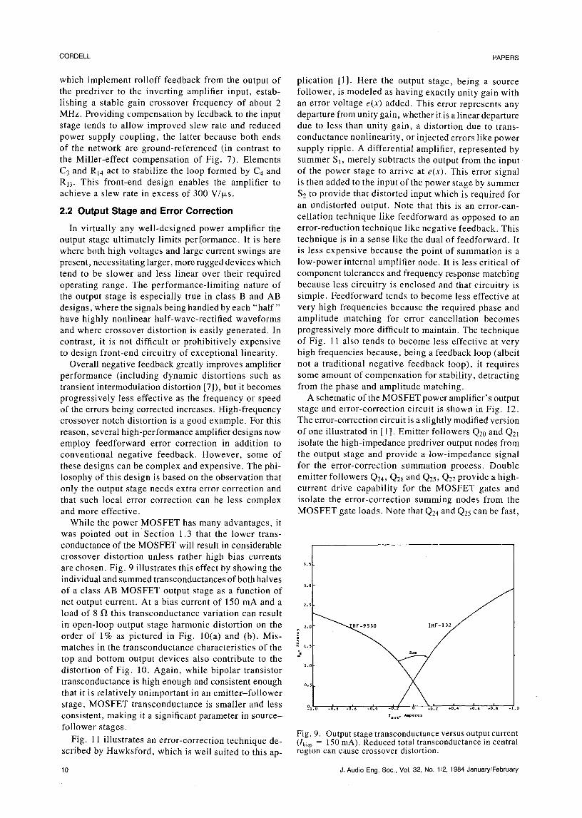
crossover distortion unless rather high bias currentsare chosen. Fig. 9 illustrates this effect by showing the "'individual and summed transconductances of both halves
5.0
of a class AB MOSFET output stage as a function ofnet output current. At a bias current of 150 mA and a z._load of 8 Il this transconductance variation can result
in open-loop output stage harmonic distortion on the _._order of 1% as pictured in Fig. 10(a) and (b). Mis- imatches in the transconductance characteristics of the _ "'
top and bottom output devices also contribute to the 'distortion of Fig. 10. Again, while bipolar transistor ,.ctransconductance is high enough and consistent enough 0.,that it is relatively unimportant in an emitter-follower
I I I I I I Istage, MOSFET transconductance is smaller and less , 0 00' ' '_ _/-6-_... _.0'. _ .. z.o'.,..'.,0 .0'.8 .,.0consistent, making it a significant parameter in source- 'ou,,A.,....
follower stages. Fig. 9. OutputstagetransconductanceversusoutputcurrentFig. 1 1 illustrates an error-correction technique de- (/bias ---- 150 mA). Reduced total transconductance in central
scribed by Hawksford, which is well suited to this ap- region can cause crossover distortion.
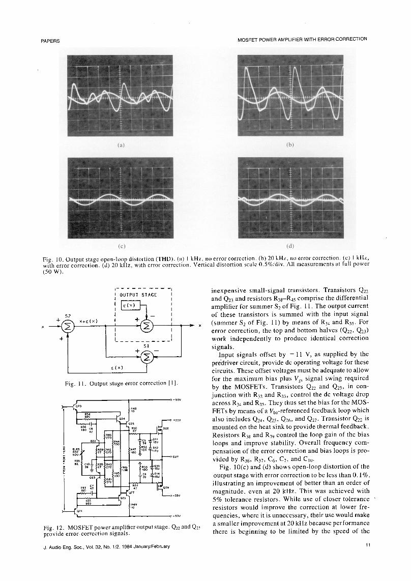
Fig. 10. Output stage open-loop distortion (THD). (a) 1 kHz, no error correction. (b) 20 kHz, no error correction. (c) I kHz,with error correction. (d) 20 kHz, with error correction. Vertical distortion scale 0.5%/div. All measurements at full power(50 w).
inexpensive small-signal transistors. Transistors Q22I OUTPUT STAGEand Q23 and resistors R38-R45 comprise the differential
I c(_ amplifier for summerS2of Fig. 11 The output currentI
s2 I +__ of these transistors is summedwith the input signal_t" _ ×+c(×) I i _ × (summerS20fFig. ll) by means of R34 and R35. For
× _ J I i error correction, the top and bottom halves (Q22, Q23)I I
+ I............ , work independently to produce identical correctionsi signals.
+[J'_"'_--- Input signals offset by -+11 V, as supplied by thepredriver circuit, provide dc operating voltage for these
z (×) circuits. These offset voltages must be adequate to allowfor the maximum bias plus Vgs signal swing required
Fig. 11. Output stage error correction [ 1]. by the MOSFETs. Transistors Q22 and Q23, in con-junction with R32 and R33, control the dc voltage drop
_2o o.,ov across R34 and R35. They thus set the bias for the MOS-
,3. :_48 FETs by means of a VbeIreferenced feedback loop which
6oo_ o2, _ .... also includes Q24,Q25,Q26,and Q27-Transistor Q22is,8oi_, _,o 0_8 mounted on the heat sink to provide thermal feedback.
i___,_ Resistors R38and R39 control the loop gain of the bias
0_2 ,, 0; loops and improve stability. Overall frequency com-R§2 Dt
_ _o'_6"8 ,:"_' _oo _ pensation of the error correction and bias loops is pro-,,, = .... vided by R36, R37, C 6, C7, and Cio.
.... Fig. 10(c) and (d) showsopen-loop distortion of the_8_ 100 t.'
i i_ _ outputstagewith errorcorrectiontobelessthan0.1%,
°_ ,-_.'[ T illustrating an improvement of better than an order of
,6o °_' ---o-_,v magnitude, even at 20 kHz. This was achieved with
_,_ °_ _/ 5% tolerance resistors. While use of closer tolerance '· resistors would improve the correction at lower fre-t__ o-_ov quencies, where it is unnecessary, their use would make
Fig. 12. MOSFET power amplifier output stage. Q22 and Q23 a smaller improvement at 20 kHz because performanceprovide error-correctionsignals, there is beginning to be limited by the speed of the
error-correction loop. Sensitivity of 20-kHz to tolerance of the noninverting amplifier under test down to thatin the error correction circuit has been measured to be of the input, subtracts the two, reintroduces 11% of
approximately 0.0002% per percent in the closed-loop the scaled-down amplifier output signal, and finallyamplifier. For ultimate performance, a pot can be placed multiplies the result by 9 for presentation to the mea-between the junctions of R38, R39 and R44, R45. suring equipment. The net effect is to provide unity
The output stage is completed by Ca, C9, and Rs0- gain for the fundamental and a gain of 10 to distortionR53 for control of parasitic oscillations and Dll-D14 products generated by the amplifier under test. Am-
for protection of the MOSFET gates from excessive plitude andPhase balance adjustments were incorporateddrive voltages. As mentioned in Section 1.6, power into the output signal path prior to the subtraction toMOSFETs are considerably more prone to high-fre- achieve a fundamental null of greater than 60 dB toquency parasitic oscillations than bipolar power tran- frequencies beyond 20 kHz. The excellent noise and
sistors because of their inherent high-speed nature and distortion performance of the 5534-type operationalbecause of their substantial drain-source capacitance, amplifiers employed make this approach effective.making it easy to form an efficient Colpitts oscillator To measure harmonic distortion, for example, a sen-structure with inductance in the gate circuit. The amount sitive THD analyzer [16] with a 20-kHz measurementof series gate resistance required for suppression of floor of about 0.001% was employed in combinationparasitic oscillations grows in proportion to the amount with this distortion magnifier to achieve a residual ofof inductance in the gate circuit. For high-speed output about 0.0003% at 20 kHz, primarily limited by noisestage operation it is therefore important to minimize of the power amplifier under test. The distortion outputthis inductance. Although not employed in Fig. 12, of the analyzer was then observed with both an oscil-this can be done especially well by shielding the gate loscope and a spectrum analyzer. The latter furtherleads back to the driver transistors, grounding the shield improves the measurement floor in most cases. Mostto the local bypass ground at each end. Then only a of the other distortion tests employed a similar ar-10-_ series resistor at the driver end and a ferrite bead rangement. Due to an oscilloscope calibration error,at the gate end are necessary, all vertical deflections in the figures are 6.4% low.
3 AMPLIFIER PERFORMANCE 3.2 Harmonic and SMPTE IntermodulationDistortion
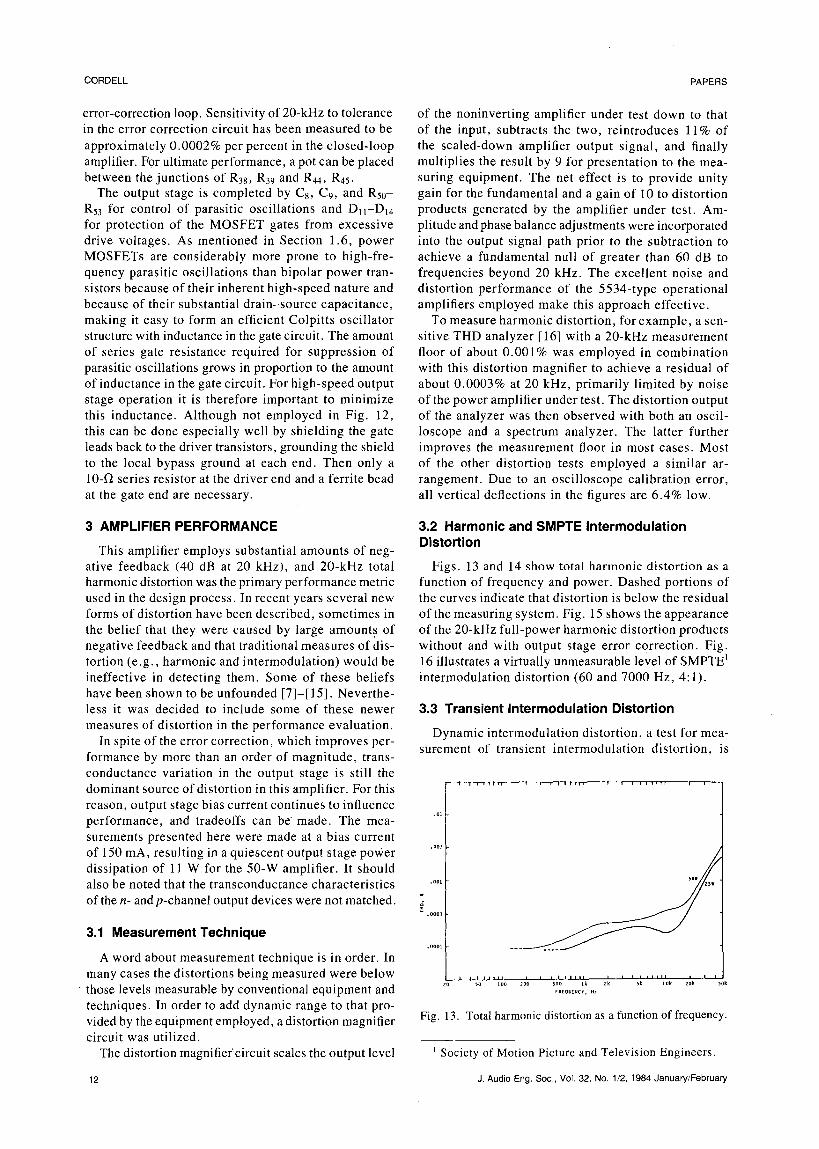
This amplifier employs substantial amounts of neg-ative feedback (40 dB at 20 kHz), and 20-kHz total Figs. 13 and 14 show total harmonic distortion as aharmonic distortion was the primary performance metric function of frequency and power. Dashed portions ofused in the design process. In recent years several new the curves indicate that distortion is below the residualforms of distortion have been described, sometimes in of the measuring system. Fig. 15 shows the appearancethe belief that they were caused by large amounts of of the 20-kHz full-power harmonic distortion productsnegative feedback and that traditional measures of dis- without and with output stage error correction. Fig.tortion (e.g., harmonic and intermodulation) would be 16 illustrates a virtually unmeasurable level of SMPTE 1ineffective in detecting them. Some of these beliefs intermodulation distortion (60 and 7000 Hz, 4:1).have been shown to be unfounded [7]-[15]. Neverthe-less it was decided to include some of these newer :3.3 Transient Intermodulation Distortion
measures of distortion in the performance evaluation. Dynamic intermodulation distortion, a test for mea-In spite of the error correction, which improves per- surement of transient intermodulation distortion, is
formance by more than an order of magnitude, trans-conductance variation in the output stage is still the
dominant source of distortion in this amplifier. For this [ ........................... [reason, output stage bias current continues to influence [performance, and tradeoffs can be'_made. The mea- '°'surements presented here were made at a bias current
.oo_
of 150mA,resultingina quiescentoutputstagepower Zdissipation of 1l W for the 50-W amplifier. It shouldalso be noted that the transconductance characteristics ....
of the n- andp-channel output devices were not matched· "'= .0oo3
3.1 Measurement Technique .ooo, __.__...__A word about measurement technique is in order. In
manycases the distortionsbeing measured were below ..................· those levels measurable by conventional equipment and _0 ' '/o'"'_;o _0'0' %0r,E0w,c,.,k.,...... _ _0_ _0k
techniques. In order to add dynamic range to that pro-vided by the equipment employed, a distortion magnifier Fig. 13. Total harmonic distortion as a function of frequency,circuit was utilized.
The distortion magnifier'circuit scales the output level _Society of Motion Picture and Television Engineers.
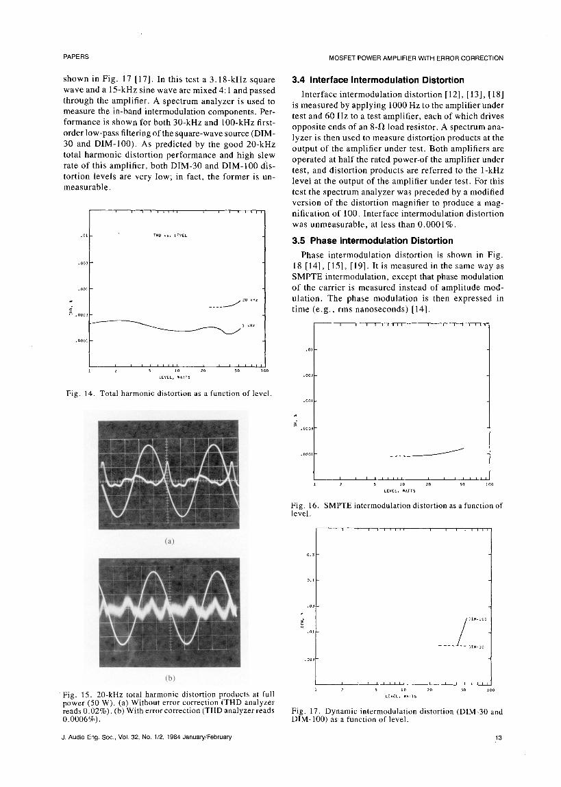
shown in Fig. 17 [17]. In this test a 3.18-kHz square 3.4 Interface Intermodulation Distortion
wave and a 15-kHz sine wave are mixed 4:1 and passed Interface intermodulation distortion [12], [13], [18]
through the amplifier. A spectrum analyzer is used to is measured by applying 1000 Hz to the amplifier undermeasure the in-band intermodulation components. Per- test and 60 Hz to a test amplifier, each of which drivesformance is shown for both 30-kHz and 100-kHz first- opposite ends of an 8-12 load resistor. A spectrum ana-order low-pass filtering of the square-wave source (DIM- lyzer is then used to measure distortion products at the30 and DIM-100). As predicted by the good 20-kHz output of the amplifier under test. Both amplifiers aretotal harmonic distortion performance and high slew operated at half the rated power_of the amplifier underrate of this amplifier, both DIM-30 and DIM-100 dis- test, and distortion products are referred to the l-kHztortion levels are very low; in fact, the former is un- level at the output of the amplifier under test. For thismeasurable, test the spectrum analyzer was precededby a modified
version of the distortion magnifier to produce a mag-................ nification of 100. Interface intermodulation distortion
was unmeasurable, at less than 0.0001%..01 THO vs. LEVEL
3.5 Phase Intermodulation Distortion
Phase intermodulation distortion is shown in Fig..... 18[14], [15], [19].It is measuredin thesamewayas
SMPTE intermodulation, except that phase modulation.... of the carrier is measuredinsteadof amplitudemod-
, ____j ..... ulation. The phase modulation is then expressed in.000., time(e.g., rmsnanoseconds)[14].
__1 kHz I I I _ I I I I I I I I I I I I I
.0001
.01
I I I I I 'Ill' 0 I0 ...... II2 5 2 50 O0
LEVEL, WATTS .003
Fig. 14. Total harmonic distortion as a function of level..001
.0003
J.0001 - -___
I I I I I I Ill I I I f i i i i
2 5 10 20 5o 100
LEVEL, _AITS
Fig. 16. SMPTE intermodulation distortion as a function oflevel.
.03
- __DIM-IO
m2
.ol
.... DIM-30
.003
I I I I I I lit I I I I I I I I
2 5 lo 20 50 100
'Fig. 15. 20-kHz total harmonic distortion products at full LEVEL,,_^_TSpower (50 W). (a) Without error correction (THD analyzerreads0.02%). (b) With error correction (THD analyzer reads Fig. 17. Dynamic intermodulation distortion (DIM-30 and0.0006%). DIM-100) as'a function of level.
3.6 Damping Factor Reactive energy stored in loudspeakers can result in
The damping factor as a function of frequency is especially serious current demands being placed on
shown in Fig. 19 and is extremely high. It is high for ampi!tiers when the loudspeaker is excited with certainthree reasons: 1) the power MOSFETs present very signals. For example, in [12] it is shown that an ordinaryclosed-box woofer alone can demand as much as 2.5light loading to the drivers, producing a low open-loopoutput impedance essentially equal to the inverse of times the peak current of a similarly rated resistive
load. Recent experimental data from real multiwaytheir transconductance; 2) the error correction circuitsystems confirm this and demonstrate that simultaneoustends to drive this open-loop output impedance to zero;excitation of multiple drivers serving different frequency3) substantial overall negative feedback further reduces
the output impedance by an amount approximating the ranges can lead to even larger ratios, in the range offeedback factor (40 dB at 20 kHz). Inclusion of a parallel 3-6 [20].R-L network (0.5 11, 0.5 IzH) at the output in series Output current is another area in which power MOS-with the load for complete capacitive load stability FETs can excel. Fig. 20 shows a 2-cycle tone burst atwill reduce the high-frequency damping factor to 125 20 kHz with a 1% duty cycle being driven into a l-Ilat 20 kHz. loadresistorbythisamplifier.It illustratesa peakcurrent
of over 22 A. This is an extremely high current capabilityAlthough the need for this much damping factor isfor a 50-W amplifier with only one output transistordoubtful, the importance of the damping factor on theof each polarity. The use of a 20-kHz tone burst reducesfrequency response and coloration has sometimes beenthe effect of power supply sag and also serves to il-underestimated. This is explained by the fact that mostlustrate that current slew-rate limiting does not occurloudspeaker systems are designed assuming that they
will be driven by a pure voltage source (sometimes, itseems, with limitlesscurrent capability as well!). For .................example, the impedance of a nominal 4-12 system maydip to 2.5 II and rise to over 50 12 at various points
1,0
across the frequency band due to driver and crossoverresonances. A typical bipolar amplifier may have adamping factor of 100 (often less at high frequencies), 0.,resulting in frequency response deviations on the orderof 0.3 dB with such a load. Coloration due to low i
damping factor may also partly explain audible differ-ences among vacuum-tube and low-feedback designs. _
.03
3.7 Peak Output Current
While the damping factor identifies the degree of .0_control an amplifier has Over its load in a small-signalsense, the output current capability determines the de- , , , , , , ..........2 5 lO 20 50 100
gree to which that control will be enforced under large- L_vEL,w^,,ssignal conditions. A large output current capability is Fig. 18. Phase intermodulation distortion as a function ofmade necessary by many of th e same factors mentioned level. Note that phase modulation is expressed in rms na-above which make a high damping factor important, noseconds.
I I [ I I Ill [ I [ I I I Ill I [ I I I [[I ] , I t I II_
10,0oo
3000
IO0O
3oo
I I !0 I I Ill i i i i i i ill i i i i t ill I I I I I Il20 > 100 Zo0 50O lk 2k 5k 10k 20k 5ok 100k
[REQUENCY, Hz
Fig. 19. Damping factor as a function of frequency.
PAPERS MOSFET POWER AMPLIFIER WITH ERRORCORRECTION
even at this very high rate of current change. A similar 23 shows 500-kHz small-signal square waves into antest into a 0.5-11 load exhibited undistorted tone bursts 8-11 resistive load and a reactive load consisting of 1
up to peak currents of 35 A. Higher frequency tests Fl and 1 _F in series. It also shows a full-power 500-yielded undistorted current slopes in excess of 30 A kHz square wave into an 8-11 load. Few bipolar am-per microsecond. The amplifier also performed satis- plifiers would survive this test. Table 1 summarizesfactorily with a 20-Hz tone burst into a 1-11 load, but overall performance of the amplifier.the effect of power supply sag was in much greaterevidence, reducing the peak current to 18 A. 4 CONCLUSION
Power MOSFETs are capable of exceptional per-3.8 Square Waves and Reactive Loads formance when used in combination with good drive
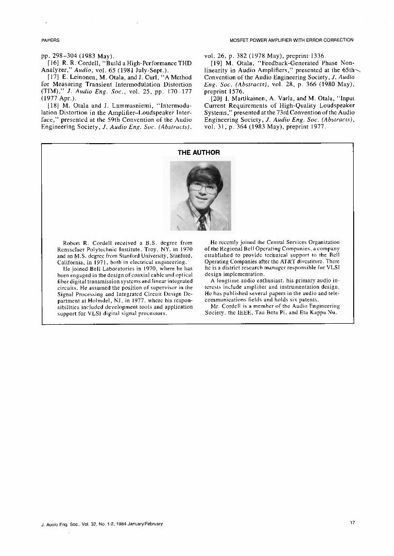
Fig. 21 illustrates small-signal and full-power 20- circuitry and simple error-correction circuitry. TheirkHz square waves into an 8-11 load. Fig. 22 shows ability to operate without complex and unreliable safe-small-signal and full-power 20-kHz square waves into area limiting circuitry makes them especially usefula reactive load consisting of 1 11 and 1 IxF in series, for demanding audio applications. Compared with bi-In the full-power case the square wave has been band- polar transistors, the major disadvantage of MOSFETslimited to 200 kHz by a first-order low-pass filter. Fig. (and source of distortion) seems to be the lower trans-
conductance, but this can be dealt with effectively bymeans of a simple error-correction circuit. Although
" a MOSFETpower amplifiercan still be expectedtocost a little more, the improved characteristics seemto justify the small premium in applications where per-formance is important.
5 REFERENCES
[il M.J. Hawksford, "Distortion Correction in Au-dio Power Amplifiers," presented at the 65th Conventionof the Audio Engineering Society, J. Audio Eng. Soc.(Abstracts), vol. 28, pp. 364-366 (1980 May), preprint1574.
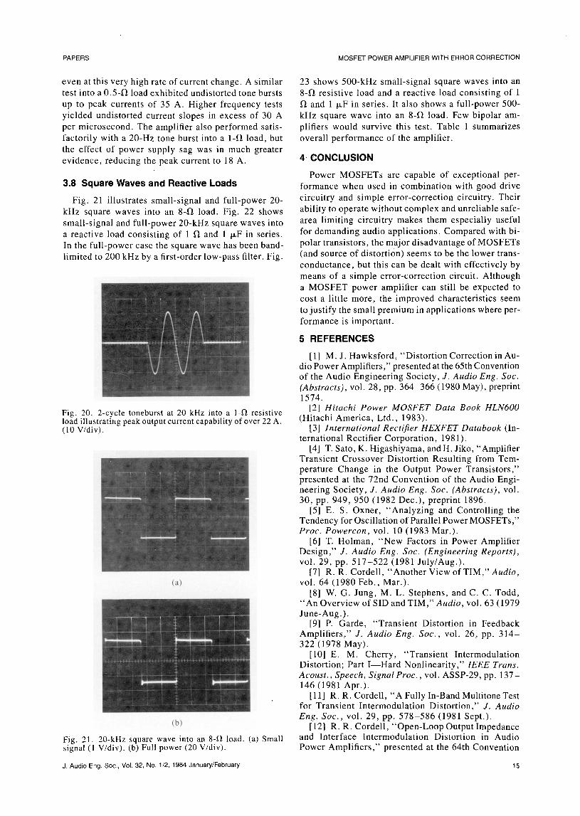
Fig. 20. 2-cycle toneburst at 20 kHz into a 1-fl resistive [2] Hitachi Power MOSFET Data Book HLN600load illustrating peak output current capability of over 22 A. (Hitachi America, Ltd., 1983).(10 V/div). [3] International Rectifier HEXFET Databook (In-
ternational Rectifier Corporation, 1981).[4] T. Sato, K. Higashiyama, and H. Jiko, "Amplifier
E Transient CrossoverDistortionResultingfrom Tem-perature Change in the Output Power Transistors,"presented at the 72nd Convention of the Audio Engi-neering Society, J. Audio Eng. Soc. (Abstracts), vol.30, pp. 949, 950 (1982 Dec.), preprint 1896.
[5] E. S. Oxner, "Analyzing and Controlling theTendency for Oscillation of Parallel Power MOSFETs,"Proc. Powercon, vol. 10 (1983 Mar.).
[6] T. Holman, "New Factors in Power AmplifierDesign," J. Audio Eng. Soc. (Engineering Reports),vol. 29, pp. 517-522 (1981 July/Aug.).
[7] R. R. Cordell, "Another View of TIM," Audio,vol. 64 (1980 Feb., Mar.).
[8] W. G. Jung, M. L. Stephens, and C. C. Todd,"An Overview of SID and TIM," Audio, vol. 63 (1979June-Aug.).
[9] P. Garde, "Transient Distortion in FeedbackAmplifiers," J. Audio Eng. Soc., vol. 26, pp. 314-322 (1978 May).
[10] E. M. Cherry, "Transient IntermodulationDistortion; Part I--Hard Nonlinearity," IEEE Trans.Acoust., Speech, Signal Proc., vol. ASSP-29, pp. 137-146 (1981 Apr.).
[11] R. R. Cordell, "A Fully In-Band Multitone Testfor Transient Intermodulation Distortion," J. AudioEng. Soc., vol. 29, pp. 578-586 (1981 Sept.).
[12] R. R. Cordell, "Open-Loop Output ImpedanceFig. 21. 20-kHz square wave into an 8-11 load. (a) Small and Interface Intermodulation Distortion in Audiosignal (1 V/div). (b) Full power (20 V/div). Power Amplifiers," presented at the 64th Convention
Slew rate >300 V/_sRisetime 100nsDamping factor, 20 Hz to 20 kHz >5000Signal-to-noise ratio, A-weighted, re 108 dB
1W
* Below measurement floor.
of the Audio Engineering Society, J. Audio Eng. Soc.(Abstracts), vol. 27, p. 1022 (1979 Dec.), preprint1537.
[13] E. M. Cherry and G. K. Cambrell, "OutputResistance and Intermodulation Distortion of Feedback
Amplifiers," J. Audio Eng. Soc., vol. 30, pp. 178-191 (1982 Apr.).
[14] R. R. Cordell, "Phase Intermodulation Dis-Fig. 22. 20-kHz square wave into a 1-fl resistor in series tortion--Instrumentation and Measurements," J. Audio
with a 1-txF capacitor. (a) Small signal (1 V/div). (b) Full Eng. Soc. vol. 31, pp. 114-124 (1983 Mar.).power (input bandlimited to 200 kHz). Top trace--20 V/div;bottom trace--output current at 20 A/div, time-base--10 txs/ [ 15] E. M. Cherry, "Amplitude and Phase of Inter-div. modulation Distortion," J. Audio Eng. Soc., vol. 31,
Fig. 23. 500-kHz square wave response. (a) Small signal, 8-fi load (1 V/div). (b) Small signal, 1 12 and 1 IxF series load (1V/div). (c) Full power, 8-12 load (20 V/div). Time base--0.5 Ixs/div.
16 J. AudioEng.Soc.,VoL32, No.1/2,1984January/February
PAPERS MOSFETPOWERAMPLIFIERWITHERRORCORRECTION
pp. 298-304 (1983 May). vol. 26, p. 382 (1978 May), preprint 1336.[16] R.R. Cordell, "BuildaHigh-PerformanceTHD [19] M. Otala, "Feedback-Generated Phase Non-
Analyzer," Audio, vol. 65 (1981 July-Sept.). linearity in Audio Amplifiers," presented at the 65th_..[ 17] E. Leinonen, M. Otala, and J. Curl, "A Method Convention of the Audio Engineering Society, J. Audio
for Measuring Transient Intermodulation Distortion Eng. Soc. (Abstracts), vol. 28, p. 366 (1980 May),(TIM)," J. Audio Eng. Soc., vol. 25, pp. 170-177 preprint 1576.(1977 Apr.). [20] I. Martikainen, A. Varla, and M. Otala, "Input
[18] M. Otala and J. Lammasniemi, "Intermodu- Current Requirements of High-Quality Loudspeakerlation Distortion in the Amplifier-Loudspeaker Inter- Systems," presented at the 73rd Convention of the Audioface," presented at the 59th Convention of the Audio Engineering Society, J. Audio Eng. Soc. (Abstracts),Engineering Society, J. Audio Eng. Soc. (Abstracts), vol. 31, p. 364 (1983 May), preprint 1977.
THE AUTHOR
Robert R. Cordell received a B.S. degree from He recently joined the Central Services OrganizationRensselaer Polytechnic Institute, Troy, NY, in 1970 of the Regional Bell Operating Companies, a companyand an M.S. degree from Stanford University, Stanford, established to provide technical support to the BellCalifornia, in 1971, both in electrical engineering. Operating Companies after the AT&T divestiture. There
He joined Bell Laboratories in 1970, where he has he is a district research manager responsible for VLSIbeen engaged in the design of coaxial cable and optical design implementation.fiber digital transmission systems and linear integrated A longtime audio enthusiast, his primary audio in-circuits. He assumed the position of supervisor in the terests include amplifier and instrumentation design.Signal Processing and Integrated Circuit Design De- He has published several papers in the audio and tele-partment at Holmdel, NJ, in 1977, where his respon- communications fields and holds six patents.sibilities included development tools and application Mr. Cordell is a member of the Audio Engineeringsupport for VLSI digital signal processors. Society, the IEEE, Tau Beta Pi, and Eta Kappa Nu.
J. AudioEng.Soc.,Vol.32, No.1/2,1984January/February 17