LaunchPad, MSP432, MSP430 are trademarks of Texas Instruments.ARM, Cortex are registered trademarks of ARM Ltd.
Application ReportSLAA681–May 2016
BPSK Modem Implementation With MSP432™ MCUs
Harry Qiu ........................................................................................................ MSP Applications Team
ABSTRACTThis application report introduces how to implement a 125-kbps BPSK modem by taking advantage of theCMSIS DSP Library with on-chip timer and 1-Msps ADC on the MSP432P401R. The MSP-EXP432P401RLaunchPad™ development kit is used as the main development platform.
Source code and related collateral discussed in this document can be downloaded fromhttp://www.ti.com/lit/zip/slaa681.
Contents1 Introduction ................................................................................................................... 22 BPSK Modem Algorithm .................................................................................................... 23 Modem Implementation on MSP432 MCU ............................................................................... 34 Test and Results ............................................................................................................ 85 Conclusion .................................................................................................................. 126 References .................................................................................................................. 127 Appendix..................................................................................................................... 13
List of Figures
1 BPSK Waveform ............................................................................................................. 22 Block Diagram of BPSK Demodulation ................................................................................... 33 Block Diagram of Modulator ................................................................................................ 34 Block Diagram of Demodulator ............................................................................................ 35 Block Diagram of BPSK Modulation....................................................................................... 46 Timer_A Output Modes Used in This Application ....................................................................... 47 Flow Chart of BPSK Signal Generation by Timer_A .................................................................... 58 Data Packet Structure....................................................................................................... 69 Flow Chart of Demodulation................................................................................................ 610 FEC Encoded Data Structure .............................................................................................. 711 Magnitude and Impulse Response of FIR LPF .......................................................................... 712 Hardware Test Bench ....................................................................................................... 813 Hardware Connection Block Diagram..................................................................................... 814 BPSK Waveform Generated by Modulator ............................................................................... 915 Detailed BPSK Waveform .................................................................................................. 916 Demodulation Runtime Evaluation for FPU Use ....................................................................... 1117 FEC Test Block Diagram .................................................................................................. 11
List of Tables
1 Test Results for Modulator ................................................................................................ 102 Runtime of Each Operation in Demodulator ............................................................................ 103 Test Results for Demodulator............................................................................................. 10
1 IntroductionMany microcontroller-based applications can benefit from the use of an efficient digital signal processing(DSP) library. ARM has developed a set of functions called the CMSIS DSP Library compatible with allARM® Cortex®-M3 and Cortex-M4 processors. CMSIS DSP library is designed to use ARM assemblyinstructions specific to each Cortex-M core implementation to quickly and easily handle various complexDSP functions. The Cortex-M4 processor has all of the features and the instruction set from the Cortex-M3processor plus DSP extensions and an optional single-precision floating-point unit (FPU). Communicationalgorithms such as Binary Phase Shift Keying (BPSK) that require digital signal processing can benefitfrom CMSIS DSP especially when implemented on hardware-enabled DSP platforms such as Cortex-M4.
The MSP432™ microcontroller (MCU) family of devices is TI's latest efficient ultra-low-power mixed-signalMCUs. The MSP432 MCU family features the ARM Cortex-M4F processor in a wide configuration ofdevice options including a rich set of analog, timing, and communication peripherals, thereby catering to alarge number of application scenarios where both efficient data processing and enhanced low-poweroperation are paramount. MSP432 MCU is an ideal combination of the TI MSP430™ low-power DNA,advanced mixed-signal features, and the processing capabilities of the ARM 32-bit Cortex-M4 RISCengine. The devices ship with driver libraries and are compatible with standardized components of theARM ecosystem.
This application report introduces how to implement a 125-kbps BPSK modem by taking advantage of theCMSIS DSP Library with the on-chip timer and 1-Msps ADC on the MSP432P401R. The MSP-EXP432P401R LaunchPad development kit is used as the main development platform.
2 BPSK Modem AlgorithmBPSK is a binary digital modulation scheme that conveys data by modulating the phase of a referencesignal (the carrier). Binary digital modulation uses two distinct signals to represent binary digital data intwo different phases for modulation. Usually, a carrier of one phase is used to represent bit 0, while a 180degree different phase represents bit 1. As fixed phases are used for modulation, BPSK is sometimesknown as absolute binary phase shift keying to distinguish it from differential binary phase shift keying.Figure 1 shows a typical BPSK signal.
Figure 1. BPSK Waveform
In BPSK, a fixed-frequency signal is used as carrier, and the modulated information is carried by itsdifferent phases. Assuming that the carrier frequency is 100 kHz in Figure 1 with two periodic waveformsto present each bit, the baud rate is 50 kbps.
In modern communication systems, BPSK modem is widely used, because it has the best Bit Error Ratio(BER) performance in binary modulation. For more information about the BER of BPSK, see Section 7.1.
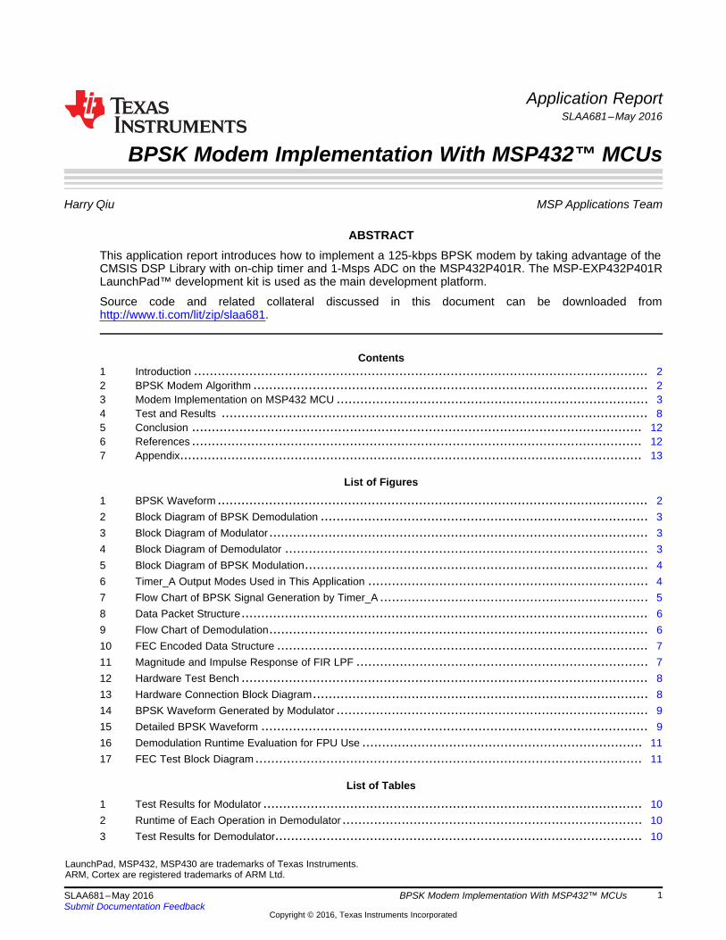
For demodulation, the receiver first recovers the clock from the received signals. The recovered clock isused to reconstruct raw data from the modulated signal by synchronous coherent demodulation. Costasloop is frequently used to recover the carrier from the modulated signal, because it is able to recover theraw data in parallel. Figure 2 shows the simple method that is applied in this application. DSP extension inCortex-M4 takes the advantages of efficiency and low power while processing many multiply operations.The ADC acquires additional dynamic range for post digital processing, which is called softwaredemodulation.
A typical application is found in an optical communication system which uses the BPSK modem method toprovide an additional path for a low-data-rate signaling link. The MSP432 MCU is selected to implementthe two-way communication.
3 Modem Implementation on MSP432 MCUThis section describes the implementation of a BPSK modem on an MSP432 MCU, including BPSKmodulation and demodulation, forward error correction (FEC) to improve BER, and digital signalconditioning.
The BPSK modulator has the following specifications:• 125-kHz carrier frequency• Up to 125-kbps bit rate• A complete packet or frame of up to 600 bytes• Using 500-kHz frequency for the ADC sampling (500 ksps), known as x4 oversampling
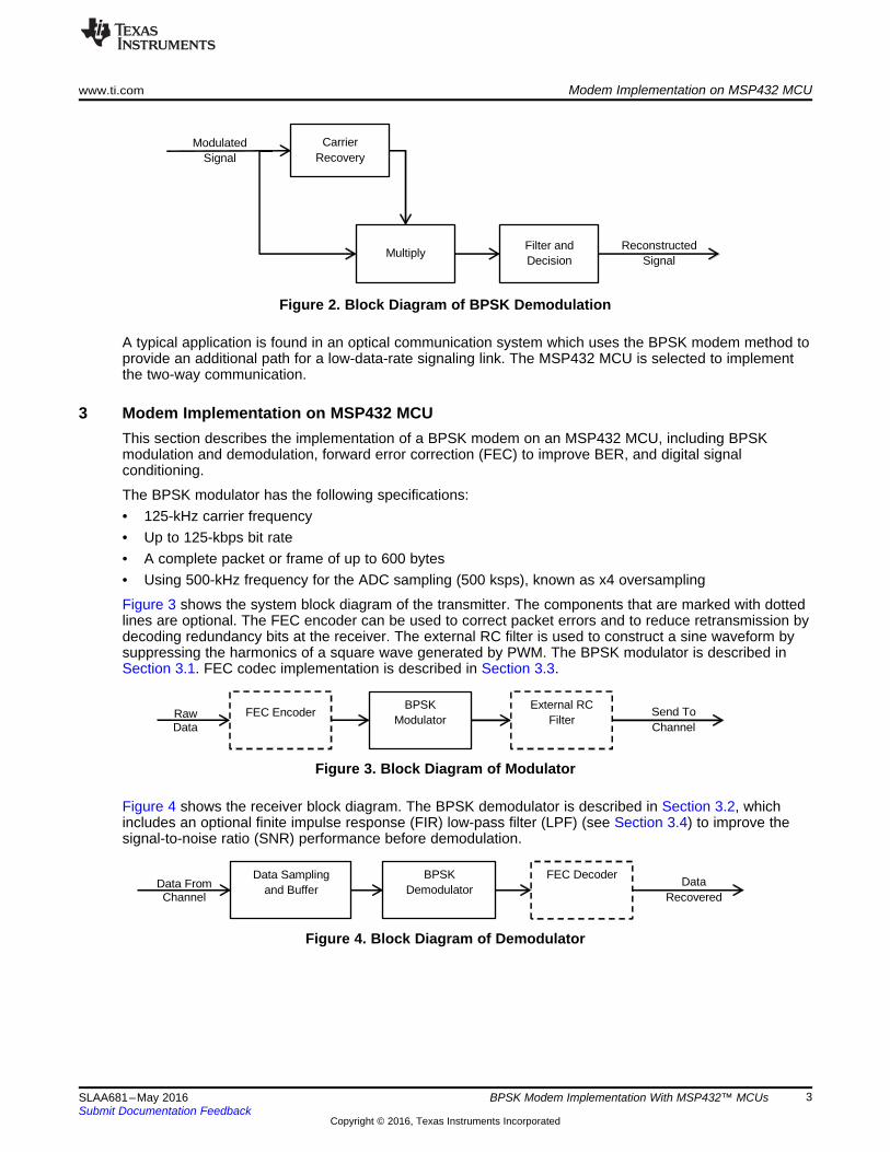
Figure 3 shows the system block diagram of the transmitter. The components that are marked with dottedlines are optional. The FEC encoder can be used to correct packet errors and to reduce retransmission bydecoding redundancy bits at the receiver. The external RC filter is used to construct a sine waveform bysuppressing the harmonics of a square wave generated by PWM. The BPSK modulator is described inSection 3.1. FEC codec implementation is described in Section 3.3.
Figure 3. Block Diagram of Modulator
Figure 4 shows the receiver block diagram. The BPSK demodulator is described in Section 3.2, whichincludes an optional finite impulse response (FIR) low-pass filter (LPF) (see Section 3.4) to improve thesignal-to-noise ratio (SNR) performance before demodulation.
3.1 Modulation ImplementationIn BPSK modulation (see Figure 5) two phases of carriers, which have a 180-degree differences, are usedto present two types of signals.
Figure 5. Block Diagram of BPSK Modulation
Section 3.1.1 describes the physical layer and data link layer implementation of BPSK modulation.
3.1.1 Physical Layer ImplementationIn the diagram in Figure 5, a timer is used in the BPSK modulator to generate the carrier that has a phasedifference of 180 degrees. In the MSP432 MCU, the Timer_A module supports several different PWMoutput modes. Output modes 2 and 6 can be configured to implement 180° phase difference in thisapplication. Figure 6 shows the phase scheme.
Figure 6. Timer_A Output Modes Used in This Application
Figure 7 shows how to generate the carrier with the Timer_A module. The clock signal is sourced fromSMCLK through a divider. Timer_A works at stop mode normally, and when transmission starts,reconfigures its state to up mode and enables the counter. When the counter value matches the value inthe TAxCCRn register, the output module is enabled and generates the output waveform. Output mode 2or mode 6 is selected by whether the bit that needs to be modulated is 0 or 1, respectively. For furtherinformation, see the MSP432P4xx Family Technical Reference Manual (SLAU356).
Figure 7. Flow Chart of BPSK Signal Generation by Timer_A
An external RC filter can be utilized to generate the sine wave for those applications that sine wave isrequired as carrier. The -3dB cut-off bandwidth is determined by Equation 1.
(1)
A 1-kΩ resistor and 1-nF capacitor are selected to achieve the 160-kHz cut-off frequency in this design.
The following pseudocode shows how the MCU implements BPSK modulation using the timer interruptand PWM output.
initial TA1 as carrier;initial TA2 as bit generator, enable interrupt;start modulation //enable carrier outputif(TA2 interrupt){
3.1.2 Data Link Layer ImplementationFigure 8 shows the packet that is defined for handshake between transmitter and receiver. To managedata transmission in burst mode, the carrier is sent ahead of the actual data to wake up the receiverbefore the date packet is sent. A data packet contains a 4-byte preamble, 1-byte delimiter, length-variablePayload Data Unit (PDU), and 1-byte checksum. The receiver acquires the bit synchronization byrecovering the clock from the preamble. Then, the receiver can identify the beginning of the PDU byrecognizing the delimiter byte. The packet ends with a checksum using Exclusive-OR. Other data integritycheck methodologies are also applicable depending on the systems requirements.
3.2 Demodulation ImplementationIn the demodulator, the ADC coverts the analog signal into digital, which provides better dynamic rangeperformance and is easier to process in software. In addition, the ADC threshold compare functionmeasures the Received Signal Strength Indicator (RSSI) and starts consecutive samplings.
In this application, because x4 oversampling is employed, the ADC sample rate is configured as 500 ksps.The threshold is set to 0.8 V as an RSSI. The ADC monitors the data line and ignores all signals below0.8 V. When the input voltage is higher than the threshold, the ADC starts to sample continuously andstore the result in SRAM using the DMA for post processing. The RSSI is averaged in parallel over awindow of every six results. When the averaged RSSI is below a preset threshold, the receiver stops ADCsampling and the post processing of the data starts.
When a complete packet is received, the clock is first recovered from the carrier and preamble of the datapacket. A mixer is used to implement the coherent demodulation with the inputs of the recovered clockand the filtered carrier. The bit sample and decision block takes the coherent result as inputs todemodulate the binary data. If the transmitter implements FEC, an FEC decoder must be applied at thereceiver to recover the raw data. Figure 9 shows the demodulation flow chart.
Figure 9. Flow Chart of Demodulation
The following pseudocode demonstrates demodulation.initialize ADC high-threshold interrupt;
//when input signal reaches RSSIif(ADC's high-threshold interrupt){
using TA1(500kHz) to sample; //start adc samplingstore data in SRAM;if((data[index] + data[index-1] + data[index-2] +data[index-3] + data[index-4] + data[index-
5]) < stopthreshold)//the window used for sampling stop decision{
recover clock from carrier sync bytes;stage1 = fir(data);//optional//synchronous coherent demodulationstage2 = stage1 * clock;stage3 = decision(stage2);recovered data = stage3;end demodulation;
}if(end demodulation)
re-initialize and wait for next data;
3.3 FEC ImplementationFEC allows constructing a more robust and efficient system by fixing the correctable error bits andreducing retransmission. An optional 5-bit redundant codec is used to correct single-bit error in every 8-bitraw data, which is called a Hamming (13, 8) code. A codeword contains 16 bits with 8-bit LSB raw data, 3-bit unused MSB bit, and 5-bit redundancy bit in the middle (see Figure 10). See Section 7.2 for moredetails.
Figure 10. FEC Encoded Data Structure
3.4 Filter Used to Improve SNRFigure 9 includes an optional FIR LPF to improve SNR performance by blocking out-of-band signals. TheFIR filter can be designed and implemented using Matlab and CMSIS DSP Library functions, respectively.According to the Nyquist sampling theorem, the normalized cut-off frequency must be higher than 0.5. A24-stage LPF is introduced with a normalized –3-dB cut-off frequency of 0.56. Figure 11 shows themagnitude response and impulse response of the filter. A phase delay of 11.5 must be managed whenusing this 24-stage filter. The filter coefficients are generated in Matlab by calling function fir1(23, 0.56).
Figure 11. Magnitude and Impulse Response of FIR LPF
This filter can be implemented by calling the FIR functions arm_fir_init_f32 and arm_fir_f32 in the CMSISDSP Library with the filter coefficients generated by Matlab.
4 Test and ResultsThis section describes the results of the MSP432 MCU BPSK experiments. All tests were performed ontwo MSP-EXP432P401R LaunchPad development kits with Code Composer Studio IDE v6.1.0.
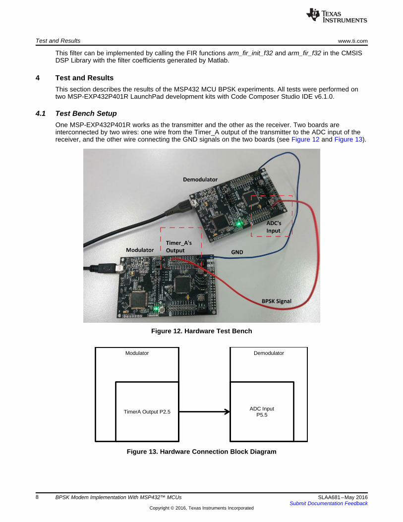
4.1 Test Bench SetupOne MSP-EXP432P401R works as the transmitter and the other as the receiver. Two boards areinterconnected by two wires: one wire from the Timer_A output of the transmitter to the ADC input of thereceiver, and the other wire connecting the GND signals on the two boards (see Figure 12 and Figure 13).
The tool versions of the software platforms are:• IDE: Code Composer Studio IDE v6.1.3• Compiler: TI ARM Compiler v5.2.7• Software Library: MSPWare v3.40.xx.xx and CMSIS v4.5.0
4.2 ModulatorFigure 14 shows the overview of a complete packet transmitted in BPSK waveform, which has a 22-msduration. Figure 15 zooms in to show the modulation at bit level. The yellow waveform represents themodulated signal, and the blue waveform represents the carrier.
The test consists of a 30-byte data transmission without FEC. The entire transmission takes 1.92 ms (30 ×8 / 125 kHz = 1.92 ms) while the CPU loading is 41.5%. For CPU loading calculation, see Section 7.3.
Figure 14. BPSK Waveform Generated by Modulator
Figure 15. Detailed BPSK Waveform
All values are specified at 125 kbps of 240-bit data without FEC encoded, with 3.3-V VCC and 48-MHzCPU clock.
Parameter Value UnitCPU use 41.5%Current consumption 7 mAFlash use 4120 bytesSRAM use 630 bytes
The complete code requires 4120 bytes plus 630 bytes for the data buffer. The system consumes 7-mAcurrent at 48 MHz and 3.3 V.
4.3 DemodulatorTransmitting a complete 210 byte encoded data requires 21.84 ms (see Table 2). In this completeconfiguration, the receiver takes 10.1 ms for demodulation and 1 ms for FEC decoding. For applicationsoperating in noise-prone environments, a FIR LPF is recommended to improve SNR. Adding the 24-stageFIR LPF filter doubles the CPU loading.
Table 2. Runtime of Each Operation in Demodulator
Operation Runtime (ms)Receiving 210-byte data with FEC encoded 21.84Demodulating without 24-stage LPF 10.124-stage LPF filtering 44.9FEC decoding 1Total 78
Table 3 lists the resources that are required for demodulation.
Table 3. Test Results for Demodulator
Parameter Value UnitCurrent consumption 7 mAFlash use 6420 bytesSRAM use 34500 bytes
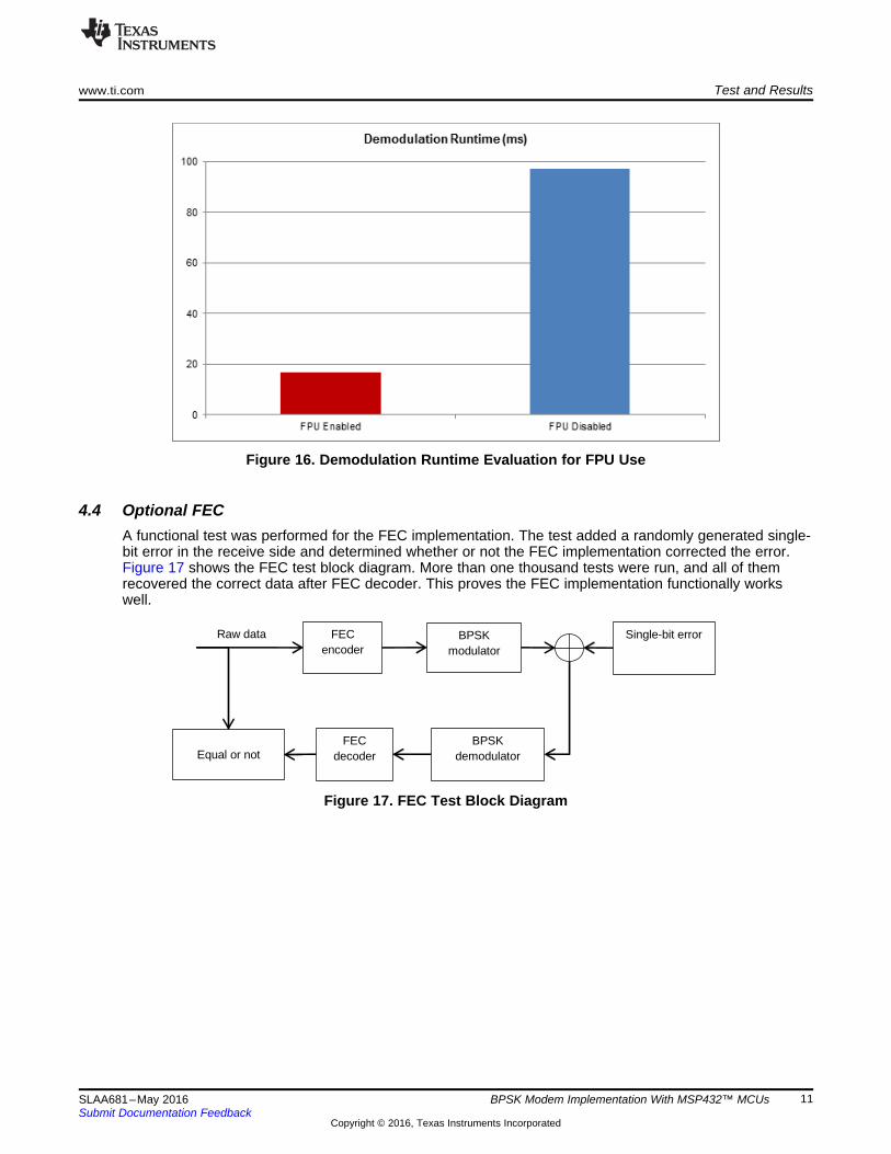
To calculate the performance advantage of the hardware FPU, an additional experiment with the FPUmodule disabled was performed. Because the CMSIS DSP Library takes advantage of the FPU, whendeactivating FPU, the implementation must use general operations instead of calling functions in theCMSIS DSP Library. In this experiment, the LPF is disabled because the FIR LPF implementation iscomplex without the use of CMSIS DSP Library functions. The runtime when using general operationswith the FPU enabled is higher than operation using the CMSIS DSP Library. This demonstrates that theCMSIS DSP Library has optimized the calculation operation by taking advantage of FPU. Figure 16 showsthe runtimes of both test conditions.
Figure 16. Demodulation Runtime Evaluation for FPU Use
4.4 Optional FECA functional test was performed for the FEC implementation. The test added a randomly generated single-bit error in the receive side and determined whether or not the FEC implementation corrected the error.Figure 17 shows the FEC test block diagram. More than one thousand tests were run, and all of themrecovered the correct data after FEC decoder. This proves the FEC implementation functionally workswell.
5 ConclusionThis application report introduces a complete design for a software-based 125-kbps BPSK modem. Thetest results show that the BPSK modem implemented on MSP432 MCU platform shows significantbenefits by taking advantage of the FPU and DSP extensions of the Cortex-M4F CPU. Complete modemfunctionality can be designed in software using the on-chip timer and ADC peripherals with minimalexternal components. This can be an effective solution for an application that requires an economic low-power space-limited solution.
6 References• MSP432P401x Mixed-Signal Microcontrollers• MSP432P4xx Family Technical Reference Manual• MSP432P401R LaunchPad Development Kit (MSP-EXP432P401R) User's Guide• Using the CMSIS DSP Library in Code Composer Studio™ for TM4C MCUs• MSP432 Peripheral Driver Library• ARM Optimizing C/C++ Compiler v5.2 User's Guide
7.1 BEREquation 2 shows the calculation of the BPSK BER.
(2)
Where erfc(x) is the complementary error function that defined as Equation 3, which is a monotonicallydecreasing function.
(3)
Where ρ is the correlation coefficient. For BPSK, ρ reaches its minimum value – 1, which makes theBPSK BER reach its minimum value.
7.2 FECAny 8-bit raw data can be encoded into 13-bit codeword by applying Hamming (13, 8) generator matrixG(x) (see Equation 4).
(4)
The Hamming (13, 8) codeword can be checked by either re-applying G(x), or by using the parity-checkmatrix H(x) (see Equation 5), where H∙G^T = 0, under the binary half-add rule, 1 + 1 = 0.
(5)
H(x) can be used to calculate if the codeword is broken, or how many bits are broken in the codeword, orwhich bit is reversed in the single-bit broken codeword. If only a single-bit error occurs in the codeword,the error can be corrected as follows.
Assuming vector x represents 8-bit raw data, y is the codeword generated using G (see Equation 6).
(6)
When a single-bit error occurs in y as y', where y' = y + e, where e is the error vector. Use H(x) to check y'(see Equation 7).
(7)
If no error occurs, that is, if e = 0 , then C = 0; if a 1-bit recoverable error occurs, the elements in e are all0 except for only one 1, and C is the one column vector of H; if 2 or more bits of unrecoverable erroroccur, more than one 1 is in e, and C is the linear combination of column vectors of H. The checksumvector C can determine if an error occurred and what kind of error occurred. C can be used to recover a 1-bit error.
7.3 CPU LoadingCPU loading is achieved by:1. Set CPU clock as 48 MHz, in addition to all other system initial settings.2. Generate the data that to be transmitted.3. Use interrupt to send the data and, while in the main loop, activate a continuous counter.4. Record the counter value (as A) at the end of transmission.5. Use a counter to count in a dummy program for the same time, and record the counter value (as N).
Texas Instruments Incorporated and its subsidiaries (TI) reserve the right to make corrections, enhancements, improvements and otherchanges to its semiconductor products and services per JESD46, latest issue, and to discontinue any product or service per JESD48, latestissue. Buyers should obtain the latest relevant information before placing orders and should verify that such information is current andcomplete. All semiconductor products (also referred to herein as “components”) are sold subject to TI’s terms and conditions of salesupplied at the time of order acknowledgment.TI warrants performance of its components to the specifications applicable at the time of sale, in accordance with the warranty in TI’s termsand conditions of sale of semiconductor products. Testing and other quality control techniques are used to the extent TI deems necessaryto support this warranty. Except where mandated by applicable law, testing of all parameters of each component is not necessarilyperformed.TI assumes no liability for applications assistance or the design of Buyers’ products. Buyers are responsible for their products andapplications using TI components. To minimize the risks associated with Buyers’ products and applications, Buyers should provideadequate design and operating safeguards.TI does not warrant or represent that any license, either express or implied, is granted under any patent right, copyright, mask work right, orother intellectual property right relating to any combination, machine, or process in which TI components or services are used. Informationpublished by TI regarding third-party products or services does not constitute a license to use such products or services or a warranty orendorsement thereof. Use of such information may require a license from a third party under the patents or other intellectual property of thethird party, or a license from TI under the patents or other intellectual property of TI.Reproduction of significant portions of TI information in TI data books or data sheets is permissible only if reproduction is without alterationand is accompanied by all associated warranties, conditions, limitations, and notices. TI is not responsible or liable for such altereddocumentation. Information of third parties may be subject to additional restrictions.Resale of TI components or services with statements different from or beyond the parameters stated by TI for that component or servicevoids all express and any implied warranties for the associated TI component or service and is an unfair and deceptive business practice.TI is not responsible or liable for any such statements.Buyer acknowledges and agrees that it is solely responsible for compliance with all legal, regulatory and safety-related requirementsconcerning its products, and any use of TI components in its applications, notwithstanding any applications-related information or supportthat may be provided by TI. Buyer represents and agrees that it has all the necessary expertise to create and implement safeguards whichanticipate dangerous consequences of failures, monitor failures and their consequences, lessen the likelihood of failures that might causeharm and take appropriate remedial actions. Buyer will fully indemnify TI and its representatives against any damages arising out of the useof any TI components in safety-critical applications.In some cases, TI components may be promoted specifically to facilitate safety-related applications. With such components, TI’s goal is tohelp enable customers to design and create their own end-product solutions that meet applicable functional safety standards andrequirements. Nonetheless, such components are subject to these terms.No TI components are authorized for use in FDA Class III (or similar life-critical medical equipment) unless authorized officers of the partieshave executed a special agreement specifically governing such use.Only those TI components which TI has specifically designated as military grade or “enhanced plastic” are designed and intended for use inmilitary/aerospace applications or environments. Buyer acknowledges and agrees that any military or aerospace use of TI componentswhich have not been so designated is solely at the Buyer's risk, and that Buyer is solely responsible for compliance with all legal andregulatory requirements in connection with such use.TI has specifically designated certain components as meeting ISO/TS16949 requirements, mainly for automotive use. In any case of use ofnon-designated products, TI will not be responsible for any failure to meet ISO/TS16949.
Products ApplicationsAudio www.ti.com/audio Automotive and Transportation www.ti.com/automotiveAmplifiers amplifier.ti.com Communications and Telecom www.ti.com/communicationsData Converters dataconverter.ti.com Computers and Peripherals www.ti.com/computersDLP® Products www.dlp.com Consumer Electronics www.ti.com/consumer-appsDSP dsp.ti.com Energy and Lighting www.ti.com/energyClocks and Timers www.ti.com/clocks Industrial www.ti.com/industrialInterface interface.ti.com Medical www.ti.com/medicalLogic logic.ti.com Security www.ti.com/securityPower Mgmt power.ti.com Space, Avionics and Defense www.ti.com/space-avionics-defenseMicrocontrollers microcontroller.ti.com Video and Imaging www.ti.com/videoRFID www.ti-rfid.comOMAP Applications Processors www.ti.com/omap TI E2E Community e2e.ti.comWireless Connectivity www.ti.com/wirelessconnectivity