26
Break Memory Wall Through Silicon Photonics Jiang Xu

Break Memory Wall Through Silicon Photonics
Jiang Xu

Acknowledgement
▪Current PhD students▪ Zhehui Wang, Peng Yang, Zhifei Wang, Duong Huu Kinh Luan, Haoran Li, Rafael Kioji VivasMaeda, Xuanqi Chen, Zhongyuan Tian
▪ Past members▪ Mahdi Nikdast, Yaoyao Ye, Zhe Wang, Weichen Liu, Xiaowen Wu, Xuan Wang, Xing Wen, KwaiHung Mo, Sébastien Le Beux, Yu Wang, Yiyuan Xie, Huaxi Gu
7/12/2017 Jiang Xu (Big Data System Lab) 2

PERFECT Computing Systems for Information Age
Performance
Energy efficiency
Reliability
Functionality
Extensibility
Cost
Testability7/12/2017 Jiang Xu (Big Data System Lab) 3

Memory Wall is a Major Issue
▪Computation and memory are physically separated and distributed▪ At node, rack, and system levels
▪Mismatch of computation, memory, communication, and support subsystems▪ More/faster processors require more and/or faster memory accesses
▪ Distributed subsystems require efficient synchronization schemes
▪Worsen by the ending of Moore’s Law▪ Cores and caches compete for limited chip area and TDP
Control
Subsystems of a
computation system
7/12/2017 Jiang Xu (Big Data System Lab) 4
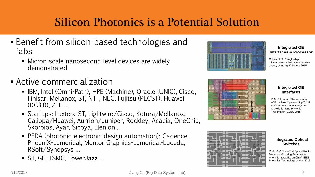
Silicon Photonics is a Potential Solution
▪ Benefit from silicon-based technologies and fabs▪ Micron-scale nanosecond-level devices are widely demonstrated
▪ Active commercialization▪ IBM, Intel (Omni-Path), HPE (Machine), Oracle (UNIC), Cisco, Finisar, Mellanox, ST, NTT, NEC, Fujitsu (PECST), Huawei (DC3.0), ZTE …
▪ Startups: Luxtera-ST, Lightwire/Cisco, Kotura/Mellanox, Caliopa/Huawei, Aurrion/Juniper, Rockley, Acacia, OneChip, Skorpios, Ayar, Sicoya, Elenion…
▪ PEDA (photonic-electronic design automation): Cadence-PhoeniX-Lumerical, Mentor Graphics-Lumerical-Luceda, RSoft/Synopsys …
▪ ST, GF, TSMC, TowerJazz …
Integrated OE
Interfaces & Processor
C. Sun et al., “Single-chip
microprocessor that communicates
directly using light”, Nature 2015
Integrated OE
Interfaces
D.M. Gill, et al., “Demonstration
of Error Free Operation Up To 32
Gb/s From a CMOS Integrated
Monolithic Nano-Photonic
Transmitter”, CLEO 2015
Integrated Optical
Switches
R. Ji, et al. “Five-Port Optical Router
Based on Microring Switches for
Photonic Networks-on-Chip”, IEEE
Photonics Technology Letters 2013
7/12/2017 Jiang Xu (Big Data System Lab) 5

Photonics is Different from Electronics
▪Advantages▪ Ultra-high bandwidth
▪ Low propagation delay
▪ Low propagation loss
▪ Low sensitivity to environmental EMI
▪Disadvantages▪ Electrical/optical conversion
▪ Thermal sensitivity
▪ Crosstalk noise
▪ Process variation
▪ Difficult to “buffer”
Differences bring opportunities and challenges
Solkan Bridge, Slovenia 1906Stone 85/220m
Cold Spring Bridge, USA 1963Steel 210/371m
Tsing Ma Bridge, Hong Kong 1997Steel 1377/2160m
7/12/2017 Jiang Xu (Big Data System Lab) 6

Outline
▪ Introduction
▪OMIN: optical memory interconnection network
▪MOCA overview
▪ Evaluation and analysis
▪Conclusions
7/12/2017 Jiang Xu (Big Data System Lab) 7

Optical Memory Interconnection Network (OMIN)
▪OMIN connects cache, local memory, and remote memory▪ Based on unified inter/intra-chip and inter-node optical network
▪ Inter- and intra-chip electrical interconnects are separately designed▪ Limited and expensive chip pins create a sharp chip boundary
▪ Different on-chip and off-chip constraints
▪ Maximize design flexibility and allow third-party system integration
▪ Co-design inter/intra-chip and inter-node network to take the full advantages of optical interconnects▪ Avoid buffering and reduce OE/EO conversions
▪ Optical chip pins offer 100X~1000X higher bandwidth than electrical chip pins*
* Z. Wang, et al., “Alleviate Chip I/O Pin Constraints for Multicore
Processors through Optical Interconnects”, ASP-DAC 2015.
7/12/2017 Jiang Xu (Big Data System Lab) 8

MOCA: Memory Optical Communication Architecture
* Z. Wang, Z. Pang, P. Yang, J. Xu, et al., “MOCA: an Inter/Intra-Chip Optical Network for Memory,” DAC 2017
7/12/2017 Jiang Xu (Big Data System Lab) 9

Intra-Chip Optical Network
▪ Segmented bidirectional optical ring
▪ Multiple simultaneous transactions on one data channel
MR
MR
PD
MR
PD
VCSELs VCSELs
Waveguide On-state MR
Photodetector Optical terminator
Optical signals
PD
MR
MR
PD
VCSELs VCSELs
MR
PD
MR
MR
MR
Off-state MRMR
Core cluster i+3 Core cluster i+2
Transceiver Transceiver
Core cluster i Core cluster i+1
Transceiver Transceiver
Waveguide
Optical
terminator
MR
Microresonator
PD
Photodetector
Core
...
...
...
...
...
...
...
...
...
...
...CA cluster
CC0
Cluster
agent i
Optical switching box
...
... MRMR
... MRMR
... PDPD
... PDPD
...
... PDPD
Interface to cluster agent
... MRMR
... MRMR
... PDPD
VCSELs
VCSELs
VCSELs
CA7CA0 CA1
...CA63CA56 CA57
CA i
CC1
CC2CC63
CC62 CC3
CC i
Core
cluster i
Co
nn
ecte
d to
CA
Optical transceiver
...
Optical transceiver
Optical receiver
... PDPDOptical receiver
Data channel 0
Data channel i
Data channel i+1
Data channel N-1
CC0 CC1 CC2 … CC(n-1) CCnCC(n-2)
CC0 CC1 CC2 … CC(n-1) CCnCC(n-2)
…CC0 CC1 CC2 … CC(n-1) CCnCC(n-2)
(a) MWSR
(b) MWMR
(c) SUOR
Continuous
wavelength
Modulated
wavelength
MOCA
7/12/2017 Jiang Xu (Big Data System Lab) 10

Physically-Centralized Logically-Distributed Control
▪Cluster agents are in the chip center▪ Optically or electrically connected with clusters
▪ Electrically connected among each other
▪Distributed control algorithm▪ Computational complexity is O(1)
▪ 0.0035mm2 and 43µW/GHz at 16nm
OE
Re
g
Decoder
De
mu
x
Buffer states
De
mu
x
Request i
Request j
... Flow
controller
Channel
collision
solver
Destination
checker
EO
Dest buffer
states
... ...
...Shared channel
states
...To other agents From other agents To/from other agents
To/from other agents
Reg Reg
Channel group 0
CC0
Channel group 1
Channel group 2
…
Core cluster i Waveguide
CC1 CC2 CC3 CC4 CC5 CC6 CC7 CC8
CC0 CC1 CC2 CC3 CC4 CC5 CC6 CC7 CC8
CC0 CC1 CC2 CC3 CC4 CC5 CC6 CC7 CC8
CC0 CC1 CC2 CC3 CC4 CC5 CC6 CC7 CC8
CC i Allowed traffic pattern
7/12/2017 Jiang Xu (Big Data System Lab) 11

Laser Source and Clock
▪Off-chip laser source▪ Shared by processors and memories
▪ On-board centralized
▪ Replaceable
▪ Improve thermal control
▪ Better energy efficiency
▪Optical clock distribution▪ Synchronize processors and memories
▪ Optical fibers distribute reference clock
▪ Low power
▪ Low skew
7/12/2017 Jiang Xu (Big Data System Lab) 12

Optical Weaving OE Interface
▪ Based on a novel optical-electrical SerDes
▪High energy efficiency
▪ Low latency
7/12/2017 Jiang Xu (Big Data System Lab) 13

Traditional Electrical Funneling OE Interface
Electrical SerDes + OE conversion
7/12/2017 Jiang Xu (Big Data System Lab) 14

Optical-Electrical SerDes
▪High-speed photonic circuit with low-speed electronic circuit
7/12/2017 Jiang Xu (Big Data System Lab) 15

Simulation Environment and Setup
▪ Simulation environment: JADE [15]
▪ Benchmarks▪ COSMIC [25]
▪ STREAM [16]
▪Component parameters▪ JADE [15]
▪ OEIL [20]
▪ Micron memory power model [19]
Parameter Value
Core 32~256 ARM-v7 cores @3GHz
I/D $ 32KB/core, private
L2 $ 128~512KB/core, shared
Cache line size 64B
Cache coherence directory-based MOSI
NoC topology ring
Technology7nm electronic die65nm photonic die
Processor
7/12/2017 Jiang Xu (Big Data System Lab) 16
Simulation Environment and Setup
Memory Optical devices
Parameter Value
Waveguide propagation loss 1 dB/cm
Waveguide crossing loss 0.1 dB
Fiber propagation loss 5x10⁻⁶dB/cm
32-way splitter excess loss 4 dB
Optical pin coupling loss 2 dB
Receiver sensitivity -20 dBm
Laser power conversion efficiency 10 dB
Laser power extinction ratio 10
Microresonator passing loss 0.2 dB
Microresonator insertion loss 1 dB
Microresonator heat tuning power 0.05 mW
Parameter Value
Organization
2 bank/rankx8 rank/transaction enginex32 transaction engine/chipx32 chip/front-end enginex32 front-end engine
Frequency 800MHz
Memory Size 8GB/chip
Schedule Policy FR-FCFS
Page Policy close-page policy
Technology14nm logic die22nm memory die65nm photonic die
7/12/2017 Jiang Xu (Big Data System Lab) 17

Delivered Memory Bandwidth and Performance
▪MOCA delivers 162% higher memory bandwidth compared to HMC for 256-core processors
▪MOCA speedups 2.6X compared to HMC for 256-core processors
▪Under STREAM benchmark [16]
7/12/2017 Jiang Xu (Big Data System Lab) 18

Latency
▪MOCA reduces latency by 75% compared to HMC for 256-core processors
▪Narrowly distributed
▪Under STREAM benchmark [16]
7/12/2017 Jiang Xu (Big Data System Lab) 19

Energy Efficiency
▪MOCA helps to save 71% energy compared to HMC in 256-core processors
▪ ENoC-based MOCA can save 37% energy
▪ Better scalability in term of energy efficiency
7/12/2017 Jiang Xu (Big Data System Lab) 20

Execution Time under Different LLC Sizes
▪ 256-core, 128~32MB shared LLC
▪MOCA offers 59% higher performance than HMC
▪MOCA can support memory-intensive applications with smaller LLC
7/12/2017 Jiang Xu (Big Data System Lab) 21

Conclusions
▪MOCA is an example of OMIN▪ Unified inter/intra-chip optical network
▪ Physically-centralized logically-distributed control
▪ Off-chip central laser source
▪ Optically distributed clock
▪ Optical weaving OE interface
▪Help to reduce on-chip cache sizes
▪ Significantly improve performance and energy efficiency
7/12/2017 Jiang Xu (Big Data System Lab) 22

Publically Released Tools
▪ Bibliography for inter/intra-chip optical networks
▪ JADE heterogeneous multiprocessor simulation environment
▪COSMIC heterogeneous multiprocessor benchmark suite
▪CLAP optical crosstalk and loss analysis platform
▪OTemp optical thermal effect modeling platform
▪OEIL optical and electrical interface and link analysis environment
▪MCSL realistic network-on-chip traffic patterns
▪ PowerSoC power delivery system analysis platform
www.ece.ust.hk/~eexu
7/12/2017 Jiang Xu (Big Data System Lab) 23

Forums and Journal Special Issue
▪OPTICS Workshop▪ Optical/PhoTonic Interconnects for Computing Systems
▪ Annually since 2015, base in Europe
www.ece.ust.hk/~eexu/OPTICS
▪ PHOTONICS Workshop▪ PHotonics-Optics Technology Oriented Networking, Information and Computing Systems
▪ Annually since 2017, base in US
www.ece.ust.hk/~eexu/PHOTONICS
▪ACM Journal of Emerging Technologies in Computing Systems▪ Special issue on silicon photonics
http://jetc.acm.org/announcements.cfm
7/12/2017 Jiang Xu (Big Data System Lab) 24

Reference
[1] A. Hadke et al., “Design and Evaluation of an Optical CPU-DRAM Interconnect," in ICCD, 2008.[2] A. N. Udipi et al., “Combining Memory and a Controller with Photonics Through 3D-stacking to Enable Scalable and Energy-efficient Systems," in ISCA, 2011.[3] S. Beamer et al., “Re-architecting DRAM Memory Systems with Monolithically Integrated Silicon Photonics," in ISCA, 2010.[4] C. Batten et al., “Building Manycore Processor-to-DRAM Networks with Monolithic Silicon Photonics," in HOTI, 2008.[5] D. Brunina et al., “An Energy-Efficient Optically Connected Memory Module for Hybrid Packet- and Circuit-Switched Optical Networks," JSTQE, vol. 19, March 2013.[6] S. L. Beux et al., “Potential and Pitfalls of Silicon Photonics Computing and Interconnect," in ISCAS, 2013.[7] W. Y. Tsai et al., “A Novel Low Gate-Count Pipeline Topology with Multiplexer-Flip-Flops for Serial Link," TCSI, vol. 59, pp. 2600-2610, Nov 2012.[8] G. Kim et al., “Memory-centric System Interconnect Design with Hybrid Memory Cubes," in PACT, 2013.[9] T. Krishna et al., ”Smart: Single-Cycle Multihop Traversals over a Shared Network on Chip," in MICRO, 2014.[10] “Hybrid Memory Cube Specification 2.0," Technical Publication, 2014.[11] J. Zhan et al., “A Unified Memory Network Architecture for In-Memory Computing in Commodity Servers," in MICRO, 2016.[12] S. Li et al., “McPAT: An Integrated Power, Area, and Timing Modeling Framework for Multicore and Manycore Architectures," in MICRO, 2009.[13] X. Wu et al., “An Inter/Intra-Chip Optical Network for Manycore Processors," TVLSI, vol. 23, pp. 678-691, April 2015.[14] C. Schow et al., “A 24-Channel, 300 Gb/s, 8.2 pJ/bit, Full-Duplex Fiber-Coupled Optical Transceiver Module Based on a Single "Holey" CMOS IC," JLT, vol. 29, pp. 542-553, Feb 2011.[15] R. K. V. Maeda et al., ”JADE: A Heterogeneous Multiprocessor System Simulation Platform Using Recorded and Statistical Application Models," in AISTECS, 2016.[16] J. D. McCalpin, “Memory Bandwidth and Machine Balance in Current High Performance Computers," TCCA, pp. 19-25, Dec. 1995.[17] P. Rosenfeld et al., “DRAMSim2: A Cycle Accurate Memory System Simulator," CAL, vol. 10, pp. 16-19, Jan 2011.[18] O. Naji et al., “A High-level DRAM Timing, Power and Area Exploration Tool," in SAMOS, 2015.[19] “Calculating Memory System Power for DDR3," Technical Publication, 2014.[20] Z. Wang et al., “Improve Chip Pin Performance Using Optical Interconnects," TVLSI, vol. 24, pp. 1574-1587, April 2016.[21] “Corning R Single-Mode Optical Fiber," Technical Publication.[22] Q. Xu et al., “Micrometre-scale Silicon Electro-optic Modulator," Nature, vol. 435, no. 7040, pp. 325-327, 2005.[23] Y. Zhang et al., “Towards Adaptively Tuned Silicon Microring Resonators for Optical Networks-on-Chip Applications,” JSTQE, vol. 20, pp. 136-149, July 2014.[24] A. Supalov et al., Optimizing HPC Applications with Intel Cluster Tools. Apress, 2014.[25] Zhe Wang et al., “A Case Study on the Communication and Computation Behaviors of Real Applications in NoC-based MPSoCs,” IEEE Computer Society Annual Symposium on VLSI, Florida, July 2014.
7/12/2017 Jiang Xu (Big Data System Lab) 25


![10700 Rockley RoadHouston, Texas 77099E-mail… · 2018. 8. 18. · For more information, please contact us: ExpotechUSA 10700 Rockley Road Houston, Texas 77099 USA 281-496-0900 [voice]](https://static.documents.pub/doc/80x56/607927e9dcfbf9558e35d932/10700-rockley-roadhouston-texas-77099e-2018-8-18-for-more-information-please.jpg)
