Broadband Parallel-Circuit Class-E Amplifier with Second HarmonicControl Circuit
Akram Sheikhi, Thian, M., & Mehrnosh Vafaee (2019). Broadband Parallel-Circuit Class-E Amplifier with SecondHarmonic Control Circuit. IEEE Transactions on Circuits and Systems II: Express Briefs, 66(6), 928-932.https://doi.org/10.1109/TCSII.2018.2874983
Published in:IEEE Transactions on Circuits and Systems II: Express Briefs
Document Version:Peer reviewed version
Queen's University Belfast - Research Portal:Link to publication record in Queen's University Belfast Research Portal
General rightsCopyright for the publications made accessible via the Queen's University Belfast Research Portal is retained by the author(s) and / or othercopyright owners and it is a condition of accessing these publications that users recognise and abide by the legal requirements associatedwith these rights.
Take down policyThe Research Portal is Queen's institutional repository that provides access to Queen's research output. Every effort has been made toensure that content in the Research Portal does not infringe any person's rights, or applicable UK laws. If you discover content in theResearch Portal that you believe breaches copyright or violates any law, please contact [email protected].
1549-7747 (c) 2018 IEEE. Personal use is permitted, but republication/redistribution requires IEEE permission. See http://www.ieee.org/publications_standards/publications/rights/index.html for more information.
This article has been accepted for publication in a future issue of this journal, but has not been fully edited. Content may change prior to final publication. Citation information: DOI 10.1109/TCSII.2018.2874983, IEEETransactions on Circuits and Systems II: Express Briefs
> REPLACE THIS LINE WITH YOUR PAPER IDENTIFICATION NUMBER (DOUBLE-CLICK HERE TO EDIT) <
1
Abstract— This paper presents the analysis and coherent design
method of a high-efficiency broadband parallel-circuit Class-E
power amplifier with second harmonic control circuit. The PA’s
broadband characteristic is achieved through analysis of the load
network using double reactance compensation technique. Using a
high power LDMOS transistor and operated from a 35 V supply
voltage, the practical PA exhibits 41.5-44.1 dBm output power and
79-82.2% drain efficiency over 115-155 MHz frequency range. The
measurement results show good agreements with the simulation
results and theory.
Index Terms—Amplifier, broadband, Class-E, harmonic trap,
high efficiency, parallel-circuit, reactance compensation.
I. INTRODUCTION
WITCHED-mode and harmonically tuned power amplifiers
(PAs) have been widely used due to their simple structure
and high efficiency characteristics, [1]-[8]. The Class-E with
shunt capacitance topology reported in [6] and analyzed in [7]
employs an ideal RF choke to provide an infinite impedance at
both fundamental and harmonic frequencies, which renders its
implementation challenging. In contrast, the parallel circuit
Class-E topology described in [8] uses a finite dc-feed
inductance, thereby offering compact size, low cost, and
improved efficiency due to lower equivalent series resistance
(ESR). Furthermore, when compared to the Class-E with shunt
capacitance, the parallel-circuit Class-E PA offers higher
maximum operating frequency and higher load resistance
leading to a lower loss due to reduced impedance
transformation ratio.
Wideband power amplifiers are required for deployment in
modern wireless communication systems to enable high data
rate transmission. Many techniques have been proposed to
increase the inherent bandwidth of the Class-E PA, [9]-[15]. A
differential wideband load transformation network was
introduced in [9]. Using a combination of a finite dc-feed
inductance and low-pass filters result in wideband Class-E
amplifiers [10]. The work in [11] proposed a broadband
lumped-element impedance matching technique that leads to
high output power and high efficiency. However, this technique
requires an additional network to transform 50Ω to the Class-
E’s optimum load resistance. Wide bandwidth can also be
achieved using reactance compensation techniques [12]-[15].
The basic circuits of the classical Class-E with shunt
capacitance and the parallel-circuit Class-E power amplifier are
Manuscript submitted March 10, 2018. Akram Sheikhi is the Faculty
Member of the Electrical Engineering Department, Lorestan University, Khorramabad, Iran (e-mail: [email protected]). Mury Thian is
R
L
C
Vcc
iR
vR
i1
v1 RL
ix
C0
L0
C
)d()c(
Ynet
RLRFC
CVcc
C0
L0
)a(
RL
C
Vcc
C0
L0
)b(
Lr
C1 L1
L2
Second
Harmonic
Trap
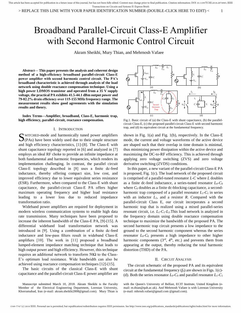
Fig.1. Basic circuit of (a) the Class-E with shunt capacitance, (b) the parallel-circuit Class-E, (c) the proposed parallel-circuit Class-E with second harmonic
trap, and (d) its equivalent circuit at the fundamental frequency.
shown in Fig. 1(a) and Fig. 1(b), respectively. In the Class-E
mode, the current and voltage waveforms of the active device
are shaped such that their overlap in time domain is minimal,
thus minimizing power dissipation within the active device and
maximizing the DC-to-RF efficiency. This is achieved through
applying zero voltage switching (ZVS) and zero voltage
derivative switching (ZVDS) conditions.
In this paper, a new variant of the parallel-circuit Class-E PA
is proposed, Fig. 1(c). The load network of the proposed circuit
is comprised of a parallel-tuned resonator L-C where L doubles
as a finite dc-feed inductance, a series-tuned resonator L0-C0
where C0 doubles as a finite dc-blocking capacitance, a second-
harmonic trap composed of a parallel resonator L1-C1 in series
with an inductor L2, and a resistor R. Compared with the
parallel-circuit Class E, our circuit incorporates a second
harmonic trap that is realized using a mixed parallel-series
resonant circuit, i.e. L1-C1-L2.This load network is analyzed in
the frequency domain using double reactance compensation
technique to maximize the bandwidth of the proposed PA. The
second harmonic trap circuit presents a low impedance to the
ground to the second harmonic component whereas the series
resonator L0-C0 presents a high impedance to other higher
harmonic components (3rd, 4th, etc.) and prevents them from
appearing at the output, thereby reducing the total harmonic
distortion (THD) of the PA.
II. CIRCUIT ANALYSIS
The circuit schematic of the proposed PA and its equivalent
circuit at the fundamental frequency (f0) are shown in Figs. 1(c)-
(d). Both the series resonator L0-C0 and parallel resonator L1-C1
with the Queen's University of Belfast, ECIT Institute, United Kingdom (e-
1549-7747 (c) 2018 IEEE. Personal use is permitted, but republication/redistribution requires IEEE permission. See http://www.ieee.org/publications_standards/publications/rights/index.html for more information.
This article has been accepted for publication in a future issue of this journal, but has not been fully edited. Content may change prior to final publication. Citation information: DOI 10.1109/TCSII.2018.2874983, IEEETransactions on Circuits and Systems II: Express Briefs
> REPLACE THIS LINE WITH YOUR PAPER IDENTIFICATION NUMBER (DOUBLE-CLICK HERE TO EDIT) <
2
are tuned at f0, thus provide a short and open circuit,
respectively. At 2f0, the resonator L1-C1 behaves like a
capacitance, which is resonated with L2 to provide a short
circuit. The circuit is analyzed using the following assumptions:
The switch is ON for 0 < ωt < π and OFF for π < ωt ≤ 2π
interval, implying a 50% duty ratio.
The output current is sinusoidal with the initial phase shift
ϕ.
To simplify the analysis with an aim to arrive at some
meaningful design insights, the transistor is modelled as an
ideal switch in parallel with a shunt capacitor C. Large
transistors typically employed in low-frequency high-power
applications such as ours have low (negligible) RON and
considerably high COFF values. Therefore, in our analysis,
only COFF is taken into account i.e. modelled as a linear
capacitance C. In [16], it was shown that it is sufficient to
approximate the nonlinear output capacitance of the
transistor with a linear capacitance.
In the analysis of the idealized parallel-circuit Class-E PA
[8], two optimum conditions, i.e., ZVS given in (1) and ZVDS
given in (2) are applied. When the transistor is turned ON,
current flows through the switch but with no voltage produced
across it. When the transistor is turned OFF, no current flows
through the switch, and the switch voltage is equal to the
voltage across the charged shunt capacitor C. Since the switch
voltage and current do not overlap, no power is dissipated
within the switch, resulting in a theoretical 100% DC-to-RF
efficiency. Two quadrature fundamental-frequency currents iR
and iX in Fig. 1(d) can be determined using Fourier integrals,
and represented as the phase angle of the load network seen
from the device drain at f0, (3).
𝑣(𝜔𝑡)|𝜔𝑡 = 2𝜋 = 0 (1)
𝑑𝑣(𝜔𝑡)
𝑑𝜔𝑡|𝜔𝑡 = 2𝜋
= 0 (2)
tan 𝜙 =𝑅
𝜔𝐿− 𝜔𝑅𝐶 (3)
The impedances of the series resonator L0-C0 and the parallel
resonator L1-C1, denoted here as Z0 and Z1 respectively, can be
expressed as
𝑍0 = 𝑗𝜔𝐿0 +1
𝑗𝜔𝐶0= 𝑗𝜔′𝐿0 (4)
𝑍1 =1
𝑗(𝜔𝐶1 − 1
𝜔𝐿1)
=1
𝑗𝜔′𝐶1 (5)
where
𝜔′ =𝜔2−𝜔0
2
𝜔 (6)
𝜔02 =
1
𝐿0𝐶0=
1
𝐿1𝐶1 (7)
The admittance of the load network, Ynet, can be expressed as
𝑌𝑛𝑒𝑡 =1
𝑗𝜔𝐿+ 𝑗𝜔𝐶 +
1
𝑍𝐴 (8)
where
𝑍𝐴 = 𝑍0 +1
1
𝑅 +
1
𝑍2
(9)
𝑍2 = 𝑗𝜔𝐿2 + 𝑍1 = 𝑗𝜔𝐿2 +1
𝑗𝜔′𝐶1 (10)
Substitutions of (4) and (10) into (9) result in
𝑍𝐴 = 𝑗𝜔′𝐿0 +𝑅 (𝜔𝜔′𝐿2𝐶1−1)
(𝜔𝜔′𝐿2𝐶1−1)−𝑗𝜔′𝑅𝐶1 (11)
𝐼𝑚 (1
𝑍𝐴) =
− (𝜔′𝑅2𝐶1𝑝 + 𝑚𝑞)
𝑅2𝑝2 + 𝑞2 (12)
where
𝑝 = (𝜔′)2𝐿0𝐶1 + 𝑚 (13a)
𝑞 = 𝜔′𝐿0𝑚 (13b)
𝑚 = 𝜔𝜔′𝐿2𝐶1 − 1 (13c)
VDD
L
C0
C1 L1
R
(a)
C
L2
L0
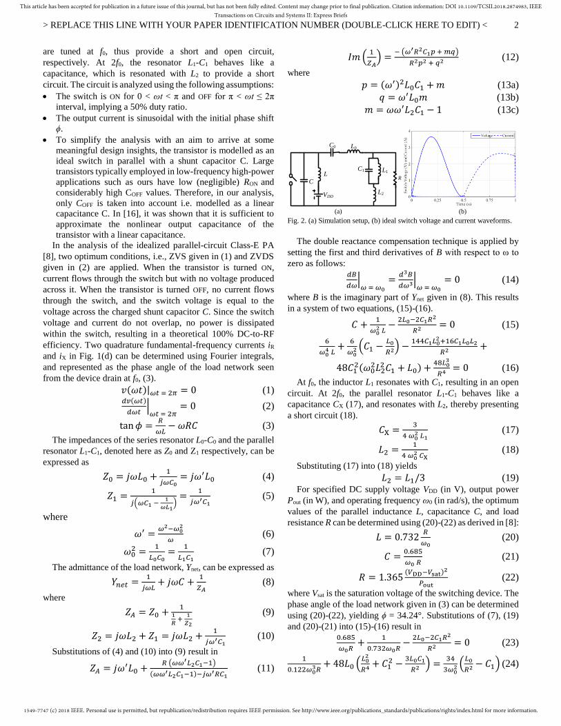
(b) Fig. 2. (a) Simulation setup, (b) ideal switch voltage and current waveforms.
The double reactance compensation technique is applied by
setting the first and third derivatives of B with respect to ω to
zero as follows:
𝑑𝐵
𝑑𝜔|
𝜔 = 𝜔0
=𝑑3𝐵
𝑑𝜔3|𝜔 = 𝜔0
= 0 (14)
where B is the imaginary part of Ynet given in (8). This results
in a system of two equations, (15)-(16).
𝐶 +1
𝜔02 𝐿
−2𝐿0−2𝐶1𝑅2
𝑅2 = 0 (15)
6
𝜔04 𝐿
+6
𝜔02 (𝐶1 −
𝐿0
𝑅2) −144𝐶1𝐿0
2 +16𝐶1𝐿0𝐿2
𝑅2 +
48𝐶12(𝜔0
2𝐿22 𝐶1 + 𝐿0) +
48𝐿03
𝑅4 = 0 (16)
At f0, the inductor L1 resonates with C1, resulting in an open
circuit. At 2f0, the parallel resonator L1-C1 behaves like a
capacitance CX (17), and resonates with L2, thereby presenting
a short circuit (18).
𝐶X =3
4 𝜔02 𝐿1
(17)
𝐿2 =1
4 𝜔02 𝐶X
(18)
Substituting (17) into (18) yields
𝐿2 = 𝐿1/3 (19) For specified DC supply voltage VDD (in V), output power
Pout (in W), and operating frequency ω0 (in rad/s), the optimum
values of the parallel inductance L, capacitance C, and load
resistance R can be determined using (20)-(22) as derived in [8]:
𝐿 = 0.732𝑅
𝜔0 (20)
𝐶 =0.685
𝜔0 𝑅 (21)
𝑅 = 1.365(𝑉DD−𝑉sat)2
𝑃out (22)
where Vsat is the saturation voltage of the switching device. The
phase angle of the load network given in (3) can be determined
using (20)-(22), yielding ϕ = 34.24°. Substitutions of (7), (19)
and (20)-(21) into (15)-(16) result in
0.685
𝜔0𝑅+
1
0.732𝜔0𝑅−
2𝐿0−2𝐶1𝑅2
𝑅2 = 0 (23)
1
0.122𝜔03𝑅
+ 48𝐿0 (𝐿0
2
𝑅4 + 𝐶12 −
3𝐿0𝐶1
𝑅2 ) =34
3𝜔02 (
𝐿0
𝑅2 − 𝐶1) (24)
1549-7747 (c) 2018 IEEE. Personal use is permitted, but republication/redistribution requires IEEE permission. See http://www.ieee.org/publications_standards/publications/rights/index.html for more information.
This article has been accepted for publication in a future issue of this journal, but has not been fully edited. Content may change prior to final publication. Citation information: DOI 10.1109/TCSII.2018.2874983, IEEETransactions on Circuits and Systems II: Express Briefs
> REPLACE THIS LINE WITH YOUR PAPER IDENTIFICATION NUMBER (DOUBLE-CLICK HERE TO EDIT) <
3
The values of L0 and C1 are determined by solving (23)-(24)
simultaneously. The values of C0, L1 and L2 are then calculated
using (7) and (19).
III. DESIGN PROCEDURES AND SIMULATIONS
In order to validate the analysis in Section II, we simulated
the PA circuit in Fig. 1(c) using an ideal switch model and ideal
passive components. The simulation setup with normalized
frequency, DC supply voltage and output power is shown in
Fig. 2(a). The switch current and voltage waveforms are shown
in Fig. 2(b), from which it can be observed that the ZVS and
ZVDS conditions are satisfied, and there is no overlap between
the switch voltage and current waveforms, leading to a high
efficiency close to 100%. The effect of variation in C on the PA
efficiency is shown in Fig. 3(a). It can be observed that the
efficiency decreases to 80% as C is increased to 1.9 × its
theoretical value in (21). Fig. 3(b) shows that when the PA is
operated in a suboptimum mode, the ZVS condition is
preserved, not affected by the S values (S=dvs/dθ). Fig. 3(c)
shows the effect that the duty ratio has on the switch voltage
and current waveforms, from which it can be observed that as
the duty ratio is increased, the peak switch voltage increases and
the peak switch current decreases.
θ (rad) 2π
No
rmal
ized
Sw
itch
Vo
ltag
e
(b)
(a)
θ (rad) 2π
No
rmal
ized
Sw
itch
Cu
rren
t
No
rmalized
Sw
itch V
oltag
e
(c)
Fig. 3. (a) PA efficiency versus normalized shunt capacitance, (b) normalized switch voltage waveforms at suboptimum and optimum operations, and (c)
normalized switch voltage and current waveforms at different duty ratio values.
The complete circuit schematic of the PA including the input
matching network and gate biasing circuit is depicted in Fig.
4(a). The transistor used in our design is a high-ruggedness n-
channel enhancement-mode lateral MOSFET (LDMOS)
MRFE6VS25N from NXP Semiconductors with a drain-source
breakdown voltage of 142 V and peak envelope power of 25 W
[17]. Using a 35 V DC supply voltage, the PA was designed to
deliver 30 W into a 50 Ω load across a 115-155 MHz frequency
range.
)b(
20 pF
120 nH
15Ω
10 Ω
100 nH
L
C
Ynet
VDD
RL
100 pF
2.7 V
)c(
)a(
L0C0
L1C1
L2
Fig. 4. (a) Complete circuit schematic of the proposed PA, (b) stability factor.
(c) real and imaginary parts of the load network’s admittance.
TABLE I LOAD-NETWORK PARAMETERS FOR POUT = 30 W AND VDD = 35 V.
Parameters L C L0 C0 L1 C1 L2
Theoretical 42.8 16.2 97 14.3 90.8 15.3 30.2
Optimized 47 10 100 14 93 16 31
The theoretical and optimized values of the PA’s load
network parameters are shown in Table I (all inductors are in
nH and capacitors are in pF). The difference between the
theoretical and optimized values of the shunt capacitor C is
mainly due to the transistor’s output capacitance, i.e. CDS = Coss
- Crss where Coss and Crss are the output and reverse transfer
capacitance of power MOSFET MRFE6VS25NR, respectively.
An L-type input matching network, comprised of a series
inductor 120 nH and a shunt capacitor 20 pF, is employed to
match the input impedance of the MOSFET to the 50 Ω source
impedance. The ESR of the 120 nH inductor, i.e. 15 Ω, helps
improve the stability of the PA, resulting in stability factor (K)
larger than 1 and stability measure (B1) larger than 0. The
stability factor of the PA is shown in Fig. 4(b). The real and
imaginary parts of the load network’s admittance, i.e. Re(Ynet)
and Im(Ynet), are plotted versus frequency in Fig. 4(c), showing
the effectiveness of the proposed load network to provide a
1549-7747 (c) 2018 IEEE. Personal use is permitted, but republication/redistribution requires IEEE permission. See http://www.ieee.org/publications_standards/publications/rights/index.html for more information.
This article has been accepted for publication in a future issue of this journal, but has not been fully edited. Content may change prior to final publication. Citation information: DOI 10.1109/TCSII.2018.2874983, IEEETransactions on Circuits and Systems II: Express Briefs
> REPLACE THIS LINE WITH YOUR PAPER IDENTIFICATION NUMBER (DOUBLE-CLICK HERE TO EDIT) <
4
constant conductance and susceptance over a wide frequency
range.
1
Dra
in C
urre
nt (
A)
Dra
in C
urre
nt (
A)
Dra
in C
urre
nt (
A)
Dra
in V
olta
ge (
V)
Dra
in V
olta
ge (
V)
Dra
in V
olta
ge (
V)
(b)
(c)
Time (ns)
(a)
Fig. 5. Simulated drain voltage and current waveforms for f0 = (a) 115 MHz,
(b) 135 MHz, and (c) 155 MHz.
Illustrated in Fig. 5 are the simulated drain voltage and
current waveforms for f0 = 115 MHz, 135 MHz, and 155 MHz,
from which it can be observed that they resemble the standard
Class-E mode waveforms. In particular, the peak drain voltage
of the 115 MHz case, i.e. 123 V, is in a good agreement with
that of the parallel-circuit Class-E where Vmax = 3.647VDD.
When simulated using the actual transistor model, an overlap
between the switch voltage and current waveforms is inevitable
due to nonidealities, packaging parasitics, etc., leading to a
degradation in efficiency. To minimize this effect, a circuit
optimization was performed using the built-in optimizer in
ADS with a chief goal to maximize the efficiency while keeping
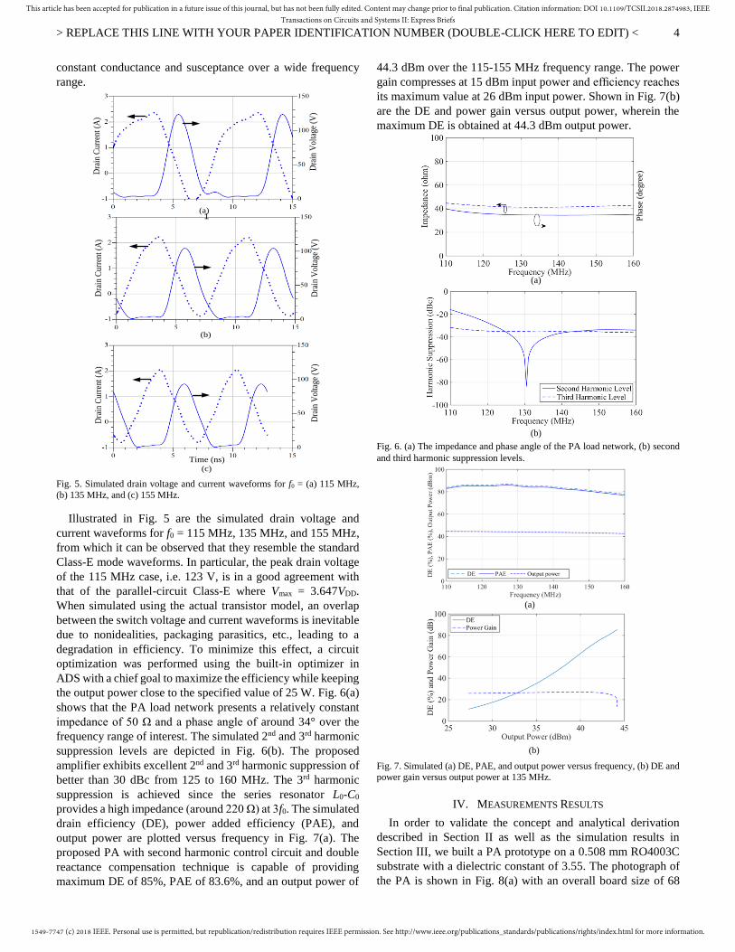
the output power close to the specified value of 25 W. Fig. 6(a)
shows that the PA load network presents a relatively constant
impedance of 50 Ω and a phase angle of around 34° over the
frequency range of interest. The simulated 2nd and 3rd harmonic
suppression levels are depicted in Fig. 6(b). The proposed
amplifier exhibits excellent 2nd and 3rd harmonic suppression of
better than 30 dBc from 125 to 160 MHz. The 3rd harmonic
suppression is achieved since the series resonator L0-C0
provides a high impedance (around 220 Ω) at 3f0. The simulated
drain efficiency (DE), power added efficiency (PAE), and
output power are plotted versus frequency in Fig. 7(a). The
proposed PA with second harmonic control circuit and double
reactance compensation technique is capable of providing
maximum DE of 85%, PAE of 83.6%, and an output power of
44.3 dBm over the 115-155 MHz frequency range. The power
gain compresses at 15 dBm input power and efficiency reaches
its maximum value at 26 dBm input power. Shown in Fig. 7(b)
are the DE and power gain versus output power, wherein the
maximum DE is obtained at 44.3 dBm output power.
Ph
ase
(deg
ree)
(a)
(b) Fig. 6. (a) The impedance and phase angle of the PA load network, (b) second
and third harmonic suppression levels.
(a)
(b)
Fig. 7. Simulated (a) DE, PAE, and output power versus frequency, (b) DE and
power gain versus output power at 135 MHz.
IV. MEASUREMENTS RESULTS
In order to validate the concept and analytical derivation
described in Section II as well as the simulation results in
Section III, we built a PA prototype on a 0.508 mm RO4003C
substrate with a dielectric constant of 3.55. The photograph of
the PA is shown in Fig. 8(a) with an overall board size of 68
1549-7747 (c) 2018 IEEE. Personal use is permitted, but republication/redistribution requires IEEE permission. See http://www.ieee.org/publications_standards/publications/rights/index.html for more information.
This article has been accepted for publication in a future issue of this journal, but has not been fully edited. Content may change prior to final publication. Citation information: DOI 10.1109/TCSII.2018.2874983, IEEETransactions on Circuits and Systems II: Express Briefs
> REPLACE THIS LINE WITH YOUR PAPER IDENTIFICATION NUMBER (DOUBLE-CLICK HERE TO EDIT) <
5
mm × 37 mm. The PA uses an MRFE6VS25N transistor with
Vsat = 2 V as a switching device and Wurth inductors. The
amplifier was driven by R&S 4320-MHz SMHU signal
generator. The output power was measured using an Agilent
Technologies 8563E spectrum analyzer. A 20-dB attenuator
was inserted between the PA and the spectrum analyzer. The
gate and drain voltages were applied using a MP3005D 30-
VDC power supply. The simulated and measured input
reflection coefficient (S11) are shown in Fig. 8(b), with a good
agreement between them being achieved. Fig. 8(c) shows the
measured output power, power gain, PAE and DE at 26 dBm
input power and 35 V supply voltage. Maximum output power
of 41.5-44 dBm, power gain 20-22 dB, PAE of 74-80.5 % and
DE of 79-82.2% are achieved over the bandwidth of interest
from 115 to 155 MHz. The comparison of our work with other
PAs is shown in Table II. Compared with other published
works, the proposed PA has better efficiency and higher output
power. Table II: Comparison with other works.
Ref f
(MHz)
FBW
(%)
Pout
(W)
η/ PAE
(%)
2nd/3rd HS
(dBc)
Technology
[11] 200-310 43 17.8 80/- - GaN FET
[12] 470-780 51 10 -/70 - LDMOS
[13] 480-730 41 10 -/70 - GaN
[14] 100-200 66 - 69/- - LDMOS
[15] 136-174 24 8 74/- - LDMOS
This
Work
115-155 30 25 82.2/80.5 -30/-30 LDMOS
(c)
C
L
L0
C0
L1
L2
C1
(a)
(b) Outp
ut P
ow
er (dB
m) an
d P
ow
er Gain
(dB
)
Fig. 8. (a) Photograph of the fabricated PA, (b) Simulated and measured S11, (c)
measured output power, power gain, PAE, and DE versus frequency.
V. CONCLUSION
A broadband parallel-circuit Class-E PA with second
harmonic control circuit has been analyzed using double
reactance compensation technique, and implemented using an
LDMOS transistor for a robust verification. The second
harmonic trap presents a low impedance to the ground to the
second harmonic component whereas the series resonator L0-C0
presents a high impedance to other higher harmonic
components (3rd, 4th, etc.), thereby reducing the total harmonic
distortion of the PA. The constructed prototype delivered a
maximum DE of 82.2 % and maximum output power of 25 W.
REFERENCES
[1] D. D. Venuto, G. Mezzina, and J. Rabaey, “Automatic 3D design for
efficiency optimization of a Class E power amplifier,” IEEE Trans.
Circuits Syst. II, Exp. Briefs, vol. 65, no. 2, pp. 201-205, Feb. 2018.
[2] A. Barakat, M. Thian, and V. Fusco, “A high-efficiency GaN Doherty
power amplifier with blended Class-EF mode and load-pull technique,”
IEEE Trans. Circuits Syst. II, Exp. Briefs, vol. 65, no. 2, pp. 151-155, Feb. 2018.
[3] P. Chen, K. Yang, and T. Zhang, “Analysis of a Class-E power amplifier
with shunt filter for any duty ratio,” IEEE Trans. Circuits Syst. II, Exp. Briefs, vol. 64, no. 8, pp. 857-861, Aug. 2017.
[4] M. Thian and V. F. Fusco, “Analysis and design of Class-E3F and
transmission-line Class-E3F2 power amplifiers,” IEEE Trans. Circuits Syst. I, Reg. Papers, vol. 58, no. 5, pp. 902-912, May 2011.
[5] M. Thian and V. F. Fusco, “Transmission-line Class-E power amplifier
with extended maximum operating frequency,” IEEE Trans. Circuits Syst. II, Exp. Briefs, vol. 58, no. 4, pp. 195-199, Apr. 2011.
[6] N. O. Sokal and A. D. Sokal, “Class E – A new class of high-efficiency
tuned single-ended switching power amplifiers,” IEEE. J. Solid-State Circuits, vol. 10, no. 3, pp. 168-176, Jun. 1975.
[7] F. H. Raab, “Idealized operation of the Class-E tuned power amplifier,”