76
Balanced Technology Extended (BTX) Chassis Design Guidelines February 2007 Revision 1.1
Balanced Technology Extended (BTX) Chassis Design Guidelines February 2007 Revision 1.1
2
INFORMATION IN THIS DOCUMENT IS PROVIDED IN CONNECTION WITH INTEL® PRODUCTS. NO LICENSE, EXPRESS OR IMPLIED, BY ESTOPPEL OR OTHERWISE, TO ANY INTELLECTUAL PROPERTY RIGHTS IS GRANTED BY THIS DOCUMENT. EXCEPT AS PROVIDED IN INTEL’S TERMS AND CONDITIONS OF SALE FOR SUCH PRODUCTS, INTEL ASSUMES NO LIABILITY WHATSOEVER, AND INTEL DISCLAIMS ANY EXPRESS OR IMPLIED WARRANTY, RELATING TO SALE AND/OR USE OF INTEL PRODUCTS INCLUDING LIABILITY OR WARRANTIES RELATING TO FITNESS FOR A PARTICULAR PURPOSE, MERCHANTABILITY, OR INFRINGEMENT OF ANY PATENT, COPYRIGHT OR OTHER INTELLECTUAL PROPERTY RIGHT. Intel products are not intended for use in medical, life saving, or life sustaining applications.
Intel may make changes to specifications and product descriptions at any time, without notice.
Designers must not rely on the absence or characteristics of any features or instructions marked "reserved" or "undefined." Intel reserves these for future definition and shall have no responsibility whatsoever for conflicts or incompatibilities arising from future changes to them.
The Intel® BTX may contain design defects or errors known as errata which may cause the product to deviate from published specifications. Current characterized errata are available on request.
Contact your local Intel sales office or your distributor to obtain the latest specifications and before placing your product order.
Intel and the Intel logo are trademarks or registered trademarks of Intel Corporation or its subsidiaries in the United States and other countries.
*Other names and brands may be claimed as the property of others.
Copyright © 2006 - 2007, Intel Corporation
3
Contents
1 Introduction ......................................................................................................................... 9 1.1 Purpose .................................................................................................................. 9 1.2 Scope/Objectives ................................................................................................... 9 1.3 Terminology.......................................................................................................... 10 1.4 Reference Documents.......................................................................................... 10
2 BTX Interface Specification: Chassis Implementation Guidance ..................................... 13 2.1 Motherboard Topside Zone Descriptions............................................................. 13 2.2 TMA Volumetric Allocation ................................................................................... 15
2.2.1 SRM Volumetric Allocation ................................................................... 16 2.3 Chassis Pan Zone Descriptions ........................................................................... 16 2.4 EMI Grounding Features ...................................................................................... 18 2.5 SRM Attach Features ........................................................................................... 19
2.5.1 SRM Guides: Front Guiding Features .................................................. 21 2.5.2 SRM Guides: Rear Guiding Features................................................... 23 2.5.3 SRM Retaining Tab .............................................................................. 23 2.5.4 SRM Retainer Slots .............................................................................. 25
2.6 Motherboard Mounting Features.......................................................................... 27 2.6.1 Motherboard Mounting Feature Design Requirements ........................ 28
2.7 Thermal Module Attach Features......................................................................... 30 2.8 Thermal Module Interface Feature....................................................................... 31
2.8.1 Thermal Module Interface Ducting Alternatives ................................... 33 2.9 Structural Design Considerations......................................................................... 33
2.9.1 Design Considerations for Failure Modes ............................................ 34 2.9.1.1 Solder Ball Failure Modes ................................................... 34
2.9.2 Chassis Stiffness Design Recommendations for Minimizing Solder Ball Failure ................................................................................................... 35 2.9.2.1 BTX Structural Design Testing Results............................... 35 2.9.2.2 Chassis Design Recommendations and Strategies for
Stiffness............................................................................... 36 2.9.2.2.1 Motherboard Mounting Feature Design .............. 38
2.9.3 Chassis Testing Procedures................................................................. 40 2.9.3.1 Tensile Test at Third Party Test House............................... 40
3 Rear Panel Design Considerations................................................................................... 43 3.1 Rear Panel Input/Output (RPIO) Considerations ................................................. 43 3.2 Power Supply Considerations .............................................................................. 44 3.3 Add-In Card Expansion Slot Mechanical Interface .............................................. 45 3.4 Structural Design Considerations......................................................................... 46
3.4.1 Rear Panel Sheet Metal Thickness ...................................................... 46 4 Chassis Vent Design......................................................................................................... 47
4
4.1 BTX System Airflow.............................................................................................. 47 4.2 Rear panel ventilation........................................................................................... 48 4.3 Inlet Ventilation..................................................................................................... 49 4.4 Inlet Vent Filter Guidance..................................................................................... 50 4.5 Exhaust Ventilation............................................................................................... 50 4.6 Front Bezel ........................................................................................................... 50
4.6.1 Inlet Ventilation ..................................................................................... 50 4.6.2 Bezel Impedance .................................................................................. 51 4.6.3 Exhaust Vent Recirculation Management ............................................ 52
4.7 Chassis Impedance.............................................................................................. 53 4.7.1 Maximum Acceptable System Impedance ........................................... 53
5 Support and Retention Module Design Guidance ............................................................ 57 5.1 Description............................................................................................................ 57 5.2 SRM Structural Performance Requirements........................................................ 57 5.3 SRM Installation ................................................................................................... 60 5.4 SRM Volumetric Keep-In Volume ........................................................................ 61 5.5 SRM Chassis Retainer Slot Mating Features ...................................................... 64 5.6 SRM Chassis Front Guide Interface Features ..................................................... 65 5.7 SRM Chassis Rear Guide Interface Features...................................................... 66 5.8 SRM Chassis Retaining Tab Interface Features.................................................. 66 5.9 SRM TMA Front Attach Feature Interface Design ............................................... 66 5.10 SRM Rear TMA Attach Interface.......................................................................... 69 5.11 SRM Motherboard Support Interface Features.................................................... 71 5.12 SRM Recess ........................................................................................................ 72 5.13 SRM Fan Cutout................................................................................................... 73 5.14 SRM Reference Design Line Drawing ................................................................. 75
5
Figures Figure 1: Motherboard Primary Side Volumetric Zones .................................................. 14 Figure 2: TMA Volumetric Zone Illustration ...................................................................... 15 Figure 3: Chassis and Motherboard Volumetric Zones .................................................... 16 Figure 4: Chassis Pan Volumetric Zone Description ........................................................ 17 Figure 5: Zone Variations Due to MB Designation .......................................................... 18 Figure 6: EMI Feature Illustration...................................................................................... 19 Figure 7: SRM Attach Features ........................................................................................ 20 Figure 8: SRM Front Guide - Guiding Surface.................................................................. 21 Figure 9: SRM Front Guide - Restraining Feature............................................................ 22 Figure 10: SRM Front Guide Option Illustration................................................................ 22 Figure 11: SRM Retaining Tab ......................................................................................... 23 Figure 12: SRM Retaining Tab Options Illustration .......................................................... 24 Figure 13: SRM Retainer Slot - Overall Size Constraint................................................... 25 Figure 14: SRM Retainer Slot - Channel Width Constraint .............................................. 26 Figure 15: SRM Retainer Slot - Channel Opening Constraint .......................................... 26 Figure 16: SRM Retaining Slot Options Illustration .......................................................... 27 Figure 17: Motherboard Size and Mounting Hole Location Illustration............................. 28 Figure 18: Motherboard Attach Keep-In .......................................................................... 29 Figure 19: Complex Restriction on Motherboard Mounting Feature: Location D ............ 29 Figure 20: Thermal Module Attach Features .................................................................... 30 Figure 21: Thermal Module Interface Opening................................................................ 31 Figure 22: Thermal Module Height and Width Illustration ................................................ 32 Figure 23: Alternate Vent Designs with Duct ................................................................... 33 Figure 24: Motherboard Flexure and Corresponding Strain on Component Solder Balls35 Figure 25: Critical Chassis Stiffness Value (Note all data is collected from Intel® 965
chipsets. Changes in interconnect technology may change recommendation) ....... 36 Figure 26: Chassis Design Recommendations for improved Stiffness ........................... 37 Figure 27: Full Round Emboss Mounting Feature............................................................ 38 Figure 28: Bridge Lance Emboss Mounting Feature ........................................................ 38 Figure 29: PEM Stud Mounting Feature ........................................................................... 39 Figure 30: Cantilever Bridge Lance Mounting Feature..................................................... 39 Figure 31: Board PEM and Cantilever Mounting Feature Stiffness Comparison ............. 40 Figure 32: Test fixture attached to SRM for the Pull Test................................................. 41 Figure 33: Rear Panel Opening Requirement .................................................................. 43 Figure 34: LFX12V Power Supply Unit ............................................................................ 44 Figure 35: CFX12V Power Supply Unit ............................................................................ 44 Figure 36: Rear Panel Add-In Card Expansion Slot Illustration........................................ 45 Figure 37: General BTX Component Layout .................................................................... 47 Figure 38: BTX Return Airflow Illustration......................................................................... 48 Figure 39: Rear Panel Ventilation Recommendations...................................................... 49 Figure 40: Bezel Ventilation and Recirculation Management Illustration ......................... 51 Figure 41: Bezel Recirculation Management Feature ...................................................... 53 Figure 42: BTX Type I System Impedance Curve ........................................................... 56 Figure 43: BTX Type II Chassis Impedance Curve ......................................................... 56 Figure 44: SRM Bending Stiffness Boundary Conditions ................................................. 59 Figure 45: SRM Stiffness - Moment of Inertia Increase.................................................... 60 Figure 46: SRM Installed In Chassis ................................................................................ 60 Figure 47: SRM Underboard Keep-In Volume.................................................................. 62 Figure 48: SRM Beyond-Board Keep-In Volume.............................................................. 63 Figure 49: SRM Retainer Slot Interface Feature Illustration............................................. 64

6
Figure 50: SRM Retainer Slot Interface Feature Illustration (Installed)............................ 64 Figure 51: Front Guide Interface Feature Illustration........................................................ 65 Figure 52: SRM Retaining Tab Interface Feature Illustration ........................................... 66 Figure 53: SRM - TMA Front Attach Feature Clearance .................................................. 67 Figure 54: TMA Front Mounting and Precising Feature Illustration.................................. 68 Figure 55: SRM: TMA Attach Slot Detail........................................................................... 68 Figure 56: SRM-TMA Interface Slot Opening ................................................................... 69 Figure 57: SRM Rear TMA Attach Feature Illustration ..................................................... 70 Figure 58: SRM Emboss Height ....................................................................................... 71 Figure 59: SRM Front Motherboard Support Interface Features...................................... 72 Figure 60: SRM Recess Illustration .................................................................................. 73 Figure 61: SRM Fan Cutout Illustration ............................................................................ 74 Figure 62: Intel Reference Design SRM Line Drawing..................................................... 76
Equations Equation 1: Maximum Acceptable System Impedance Curve Calculation in Mixed Units55 Equation 2: Maximum Acceptable System Impedance Curve Calculation in SI Units ..... 55 Equation 3: Resonant Frequency ..................................................................................... 58
Tables Table 1: BTX Motherboard Size Designations.................................................................. 27 Table 2: Minimum Inlet Vent Cumulative Open Area........................................................ 49 Table 3: MASI_I and MASI_II Effective Loss Coefficients ................................................ 55
7
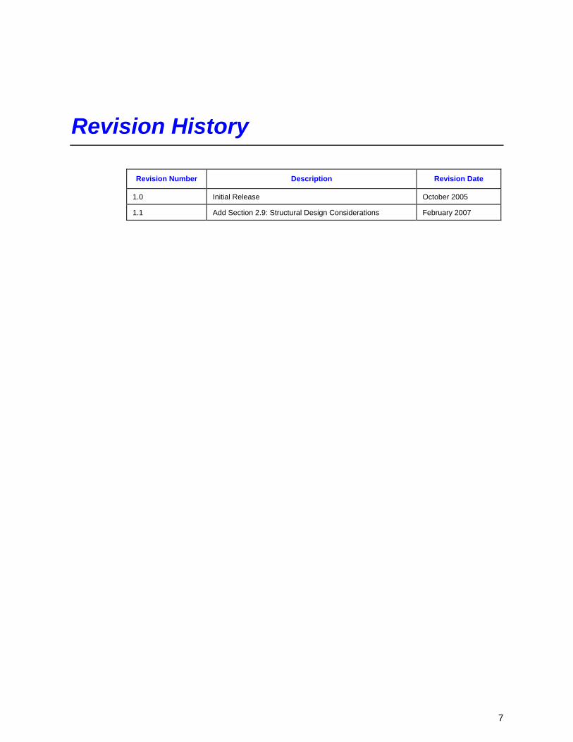
Revision History Revision Number Description Revision Date
1.0 Initial Release October 2005
1.1 Add Section 2.9: Structural Design Considerations February 2007

8
< This page is left intentionally blank >
Introduction
9
1 Introduction
1.1 Purpose The purpose of this document is to provide mechanical design guidance for Balanced Technology Extended (BTX) chassis and the Support and Retention Module (SRM) designs. This document is intended to provide guidance to BTX chassis suppliers to assist with the following:
• Identify chassis features required for BTX Interface Specification compliance
• Identify SRM features required for BTX Interface Specification compliance and Platform Design Guide compliance
• Offer practical interpretation of BTX Interface Specification requirements
• Offer chassis airflow management design practices recommendation
• Offer structural design guidance.
The purpose of this document supplements but does not replace the BTX Interface Specification.
• If there is any conflict between the information contained in this document and the BTX Interface Specification, the information in the specification takes precedence.
• The most recent versions of the BTX Interface Specification and other BTX design collateral are available at www.formfactors.org.
1.2 Scope/Objectives This document is intended to offer guidance to chassis suppliers so that they can design and manufacture chassis subassemblies in compliance with the BTX Interface Specification, and so that the chassis adequately demonstrates fundamental BTX value propositions. BTX was designed as an integrated form factor, one that took into account the needs imposed by electrical, mechanical, structural, thermal, and acoustic performance requirements and trends. As such, all BTX chassis designs should adequately demonstrate superior thermal management, cost-effective design practices, and outstanding acoustic performance.
Each section of this document will focus on different chassis and SRM design characteristics: mechanical compliance with the BTX Interface Specification, structural design recommendations, sheet metal and bezel ventilation options, and SRM design.
Introduction
10
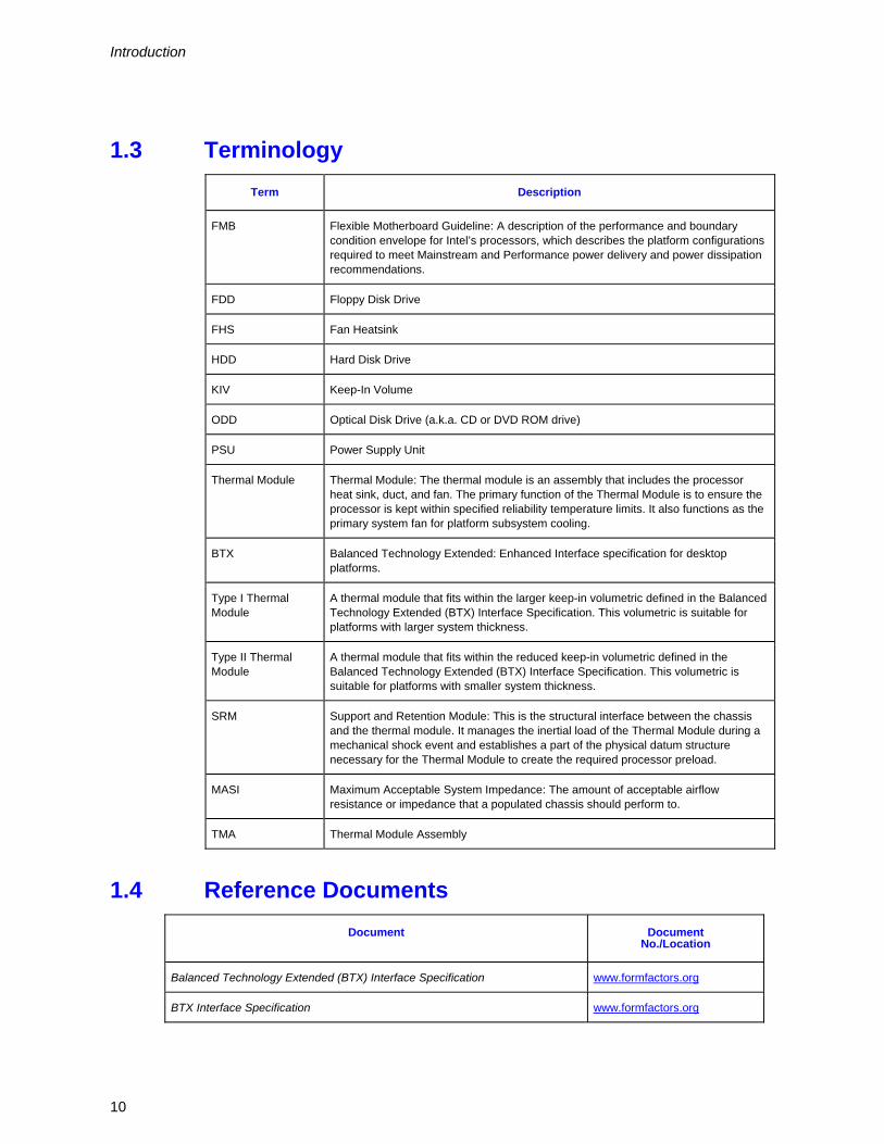
1.3 Terminology Term Description
FMB Flexible Motherboard Guideline: A description of the performance and boundary condition envelope for Intel’s processors, which describes the platform configurations required to meet Mainstream and Performance power delivery and power dissipation recommendations.
FDD Floppy Disk Drive
FHS Fan Heatsink
HDD Hard Disk Drive
KIV Keep-In Volume
ODD Optical Disk Drive (a.k.a. CD or DVD ROM drive)
PSU Power Supply Unit
Thermal Module Thermal Module: The thermal module is an assembly that includes the processor heat sink, duct, and fan. The primary function of the Thermal Module is to ensure the processor is kept within specified reliability temperature limits. It also functions as the primary system fan for platform subsystem cooling.
BTX Balanced Technology Extended: Enhanced Interface specification for desktop platforms.
Type I Thermal Module
A thermal module that fits within the larger keep-in volumetric defined in the Balanced Technology Extended (BTX) Interface Specification. This volumetric is suitable for platforms with larger system thickness.
Type II Thermal Module
A thermal module that fits within the reduced keep-in volumetric defined in the Balanced Technology Extended (BTX) Interface Specification. This volumetric is suitable for platforms with smaller system thickness.
SRM Support and Retention Module: This is the structural interface between the chassis and the thermal module. It manages the inertial load of the Thermal Module during a mechanical shock event and establishes a part of the physical datum structure necessary for the Thermal Module to create the required processor preload.
MASI Maximum Acceptable System Impedance: The amount of acceptable airflow resistance or impedance that a populated chassis should perform to.
TMA Thermal Module Assembly
1.4 Reference Documents Document Document
No./Location
Balanced Technology Extended (BTX) Interface Specification www.formfactors.org
BTX Interface Specification www.formfactors.org
Introduction
11
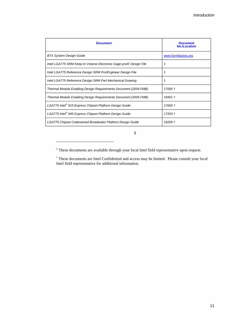
Document Document No./Location
BTX System Design Guide www.formfactors.org
Intel LGA775 SRM Keep-In Volume Electronic Gage pro/E Design File ‡
Intel LGA775 Reference Design SRM Pro/Engineer Design File ‡
Intel LGA775 Reference Design SRM Part Mechanical Drawing ‡
Thermal Module Enabling Design Requirements Document (2004 FMB) 17000 †
Thermal Module Enabling Design Requirements Document (2005 FMB) 19301 †
LGA775 Intel® 915 Express Chipset Platform Design Guide 17650 †
LGA775 Intel® 945 Express Chipset Platform Design Guide 17203 †
LGA775 Chipset Codenamed Broadwater Platform Design Guide 19259 †
§
‡ These documents are available through your local Intel field representative upon request.
† These documents are Intel Confidential and access may be limited. Please consult your local Intel field representative for additional information.

Introduction
12
< This page is left intentionally blank >
BTX Interface Specification: Chassis Implementation Guidance
13
2 BTX Interface Specification: Chassis Implementation Guidance The Balanced Technology Extended Interface Specification outlines the categories and requirements for motherboard and chassis volumetric zones. Within the specification there are examples and requirements listed for board and chassis components that typically populate each of these respective zones.
Section 2 clarifies the chassis requirements with respect to these volumetric zones and the features that the chassis must integrate to be compliant with the specification,.
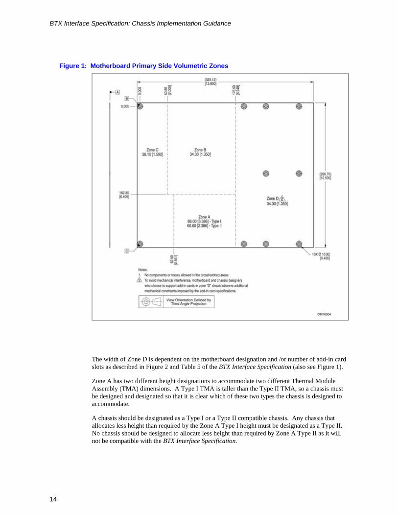
2.1 Motherboard Topside Zone Descriptions The BTX Interface Specification is written such that all chassis components and features must stay out of the volumetric zones A, B, C, D, F, G, H. Figure 1 illustrates motherboard volumetric descriptions for Zones A-D, each of which must be free of chassis components that include but are not limited to the following:
o Chassis Pan
o Chassis side walls
o Top cover
o Drive or peripheral support brackets
o Power Supply
o Power Supply Brackets
o Mechanical attach hardware (screws, rivets, seams, etc.)
BTX Interface Specification: Chassis Implementation Guidance
14
Figure 1: Motherboard Primary Side Volumetric Zones
The width of Zone D is dependent on the motherboard designation and /or number of add-in card slots as described in Figure 2 and Table 5 of the BTX Interface Specification (also see Figure 1).
Zone A has two different height designations to accommodate two different Thermal Module Assembly (TMA) dimensions. A Type I TMA is taller than the Type II TMA, so a chassis must be designed and designated so that it is clear which of these two types the chassis is designed to accommodate.
A chassis should be designated as a Type I or a Type II compatible chassis. Any chassis that allocates less height than required by the Zone A Type I height must be designated as a Type II. No chassis should be designed to allocate less height than required by Zone A Type II as it will not be compatible with the BTX Interface Specification.
BTX Interface Specification: Chassis Implementation Guidance
15
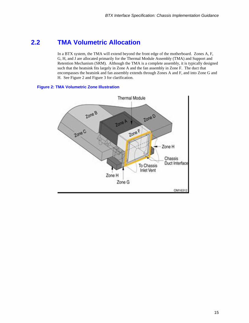
2.2 TMA Volumetric Allocation In a BTX system, the TMA will extend beyond the front edge of the motherboard. Zones A, F, G, H, and J are allocated primarily for the Thermal Module Assembly (TMA) and Support and Retention Mechanism (SRM). Although the TMA is a complete assembly, it is typically designed such that the heatsink fits largely in Zone A and the fan assembly in Zone F. The duct that encompasses the heatsink and fan assembly extends through Zones A and F, and into Zone G and H. See Figure 2 and Figure 3 for clarification.
Figure 2: TMA Volumetric Zone Illustration
BTX Interface Specification: Chassis Implementation Guidance
16
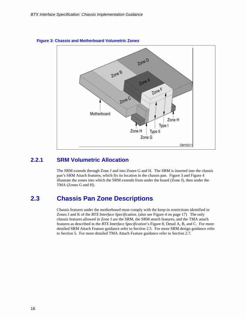
Figure 3: Chassis and Motherboard Volumetric Zones
2.2.1 SRM Volumetric Allocation
The SRM extends through Zone J and into Zones G and H. The SRM is inserted into the chassis pan’s SRM Attach features, which fix its location in the chassis pan. Figure 3 and Figure 4 illustrate the zones into which the SRM extends from under the board (Zone J), then under the TMA (Zones G and H).
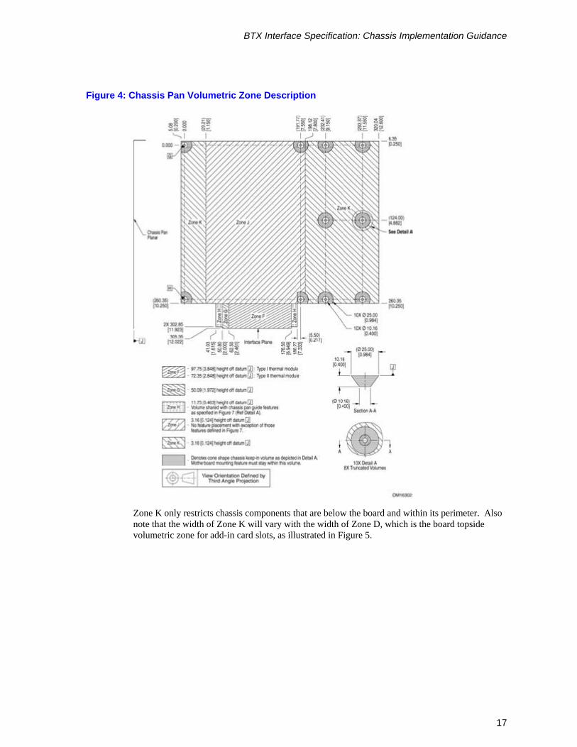
2.3 Chassis Pan Zone Descriptions Chassis features under the motherboard must comply with the keep-in restrictions identified in Zones J and K of the BTX Interface Specification. (also see Figure 4 on page 17) The only chassis features allowed in Zone J are the SRM, the SRM attach features, and the TMA attach features as described in the BTX Interface Specification’s Figure 8, Detail A, B, and C. For more detailed SRM Attach Feature guidance refer to Section 2.5. For more SRM design guidance refer to Section 5. For more detailed TMA Attach Feature guidance refer to Section 2.7.
BTX Interface Specification: Chassis Implementation Guidance
17
Figure 4: Chassis Pan Volumetric Zone Description
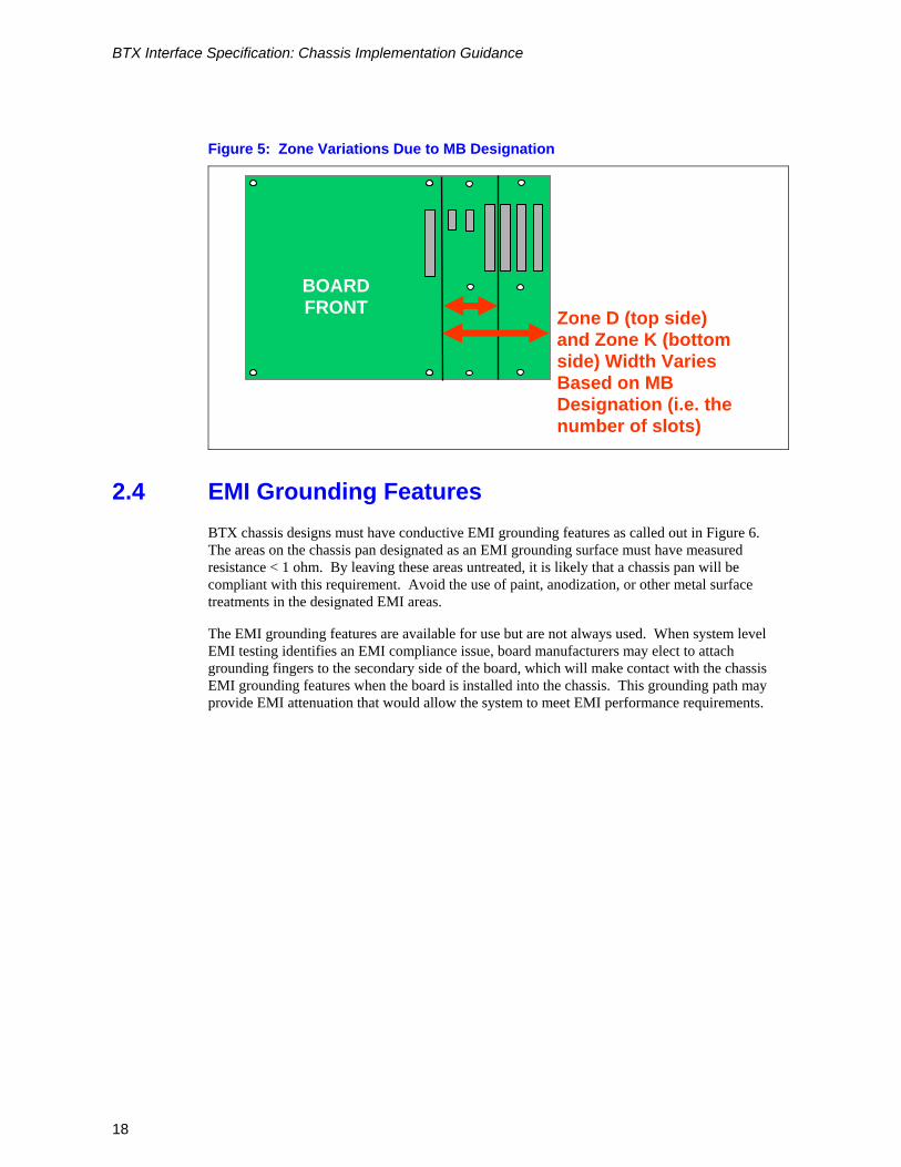
Zone K only restricts chassis components that are below the board and within its perimeter. Also note that the width of Zone K will vary with the width of Zone D, which is the board topside volumetric zone for add-in card slots, as illustrated in Figure 5.
BTX Interface Specification: Chassis Implementation Guidance
18
Figure 5: Zone Variations Due to MB Designation
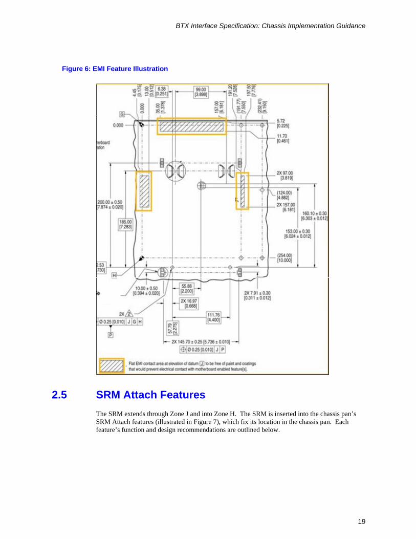
2.4 EMI Grounding Features BTX chassis designs must have conductive EMI grounding features as called out in Figure 6. The areas on the chassis pan designated as an EMI grounding surface must have measured resistance < 1 ohm. By leaving these areas untreated, it is likely that a chassis pan will be compliant with this requirement. Avoid the use of paint, anodization, or other metal surface treatments in the designated EMI areas.
The EMI grounding features are available for use but are not always used. When system level EMI testing identifies an EMI compliance issue, board manufacturers may elect to attach grounding fingers to the secondary side of the board, which will make contact with the chassis EMI grounding features when the board is installed into the chassis. This grounding path may provide EMI attenuation that would allow the system to meet EMI performance requirements.
BOARD FRONT Zone D (top side)
and Zone K (bottom side) Width Varies Based on MB Designation (i.e. the number of slots)
BTX Interface Specification: Chassis Implementation Guidance
19
Figure 6: EMI Feature Illustration
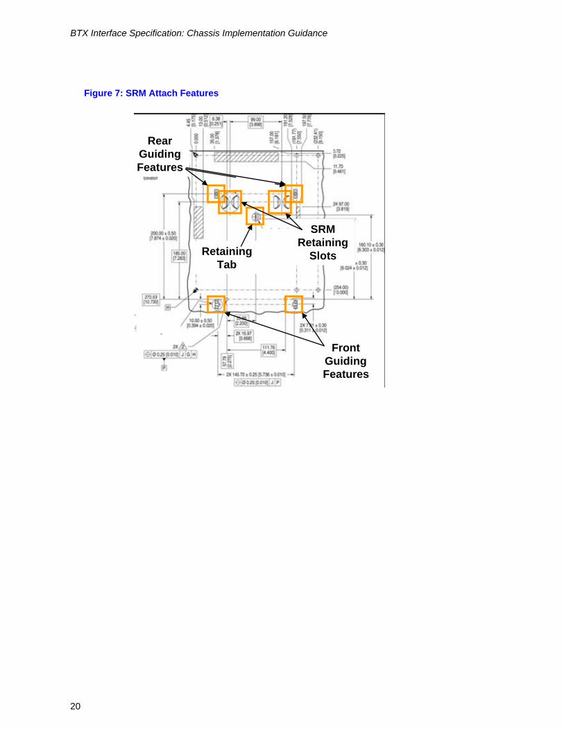
2.5 SRM Attach Features The SRM extends through Zone J and into Zone H. The SRM is inserted into the chassis pan’s SRM Attach features (illustrated in Figure 7), which fix its location in the chassis pan. Each feature’s function and design recommendations are outlined below.
BTX Interface Specification: Chassis Implementation Guidance
20
Figure 7: SRM Attach Features
FrontGuidingFeatures
RearGuidingFeatures
RetainingTab
SRMRetaining
Slots
FrontGuidingFeatures
RearGuidingFeatures
RetainingTab
SRMRetaining
Slots
FrontGuidingFeatures
RearGuidingFeatures
RetainingTab
SRMRetaining
Slots
FrontGuidingFeatures
RearGuidingFeatures
RetainingTab
SRMRetaining
Slots
BTX Interface Specification: Chassis Implementation Guidance
21
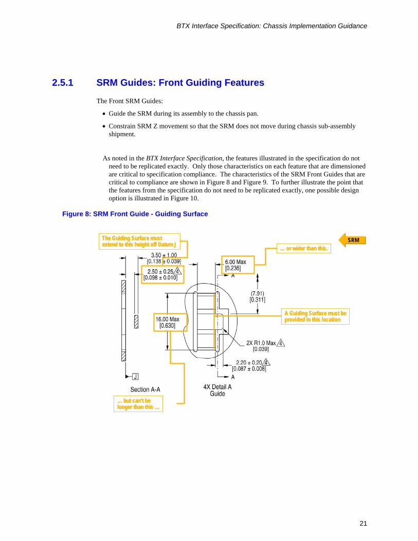
2.5.1 SRM Guides: Front Guiding Features
The Front SRM Guides:
• Guide the SRM during its assembly to the chassis pan.
• Constrain SRM Z movement so that the SRM does not move during chassis sub-assembly shipment.
As noted in the BTX Interface Specification, the features illustrated in the specification do not need to be replicated exactly. Only those characteristics on each feature that are dimensioned are critical to specification compliance. The characteristics of the SRM Front Guides that are critical to compliance are shown in Figure 8 and Figure 9. To further illustrate the point that the features from the specification do not need to be replicated exactly, one possible design option is illustrated in Figure 10.
Figure 8: SRM Front Guide - Guiding Surface
… but can’t belonger than this …
… or wider than this.
A Guiding Surface must beprovided in this location
The Guiding Surface mustextend to this height off Datum J
SRM
… but can’t belonger than this …… but can’t belonger than this …
… or wider than this.… or wider than this.
A Guiding Surface must beprovided in this locationA Guiding Surface must beprovided in this location
The Guiding Surface mustextend to this height off Datum JThe Guiding Surface mustextend to this height off Datum J
SRM
BTX Interface Specification: Chassis Implementation Guidance
22
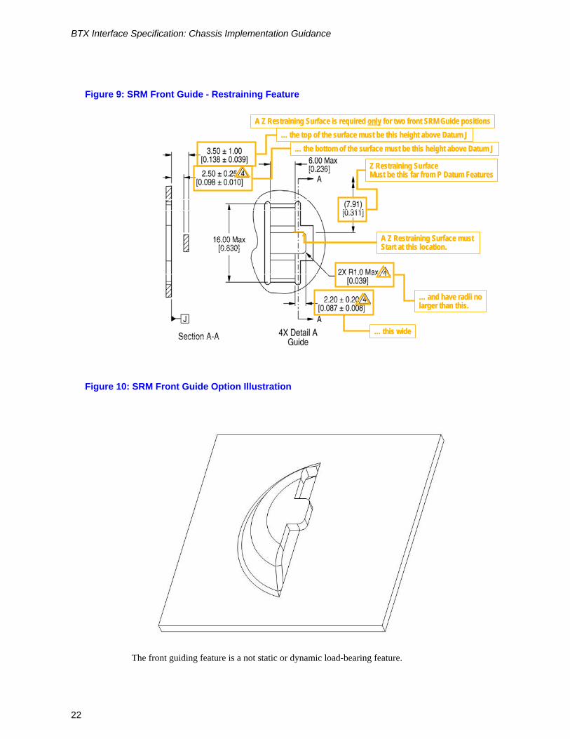
Figure 9: SRM Front Guide - Restraining Feature
A Z Restraining Surface is required only for two front SRM Guide positions
… this wide
… the bottom of the surface must be this height above Datum J… the top of the surface must be this height above Datum J
Z Restraining SurfaceMust be this far from P Datum Features
A Z Restraining Surface must Start at this location.
… and have radii nolarger than this.
A Z Restraining Surface is required only for two front SRM Guide positionsA Z Restraining Surface is required only for two front SRM Guide positions
… this wide… this wide
… the bottom of the surface must be this height above Datum J… the bottom of the surface must be this height above Datum J… the top of the surface must be this height above Datum J… the top of the surface must be this height above Datum J
Z Restraining SurfaceMust be this far from P Datum FeaturesZ Restraining SurfaceMust be this far from P Datum Features
A Z Restraining Surface must Start at this location.A Z Restraining Surface must Start at this location.
… and have radii nolarger than this.… and have radii nolarger than this.
Figure 10: SRM Front Guide Option Illustration
The front guiding feature is a not static or dynamic load-bearing feature.
BTX Interface Specification: Chassis Implementation Guidance
23
An Intel Reference Design file is available for the SRM Front Guide feature. Chassis suppliers may replicate the Intel Reference Design SRM Front Guide without restriction.
2.5.2 SRM Guides: Rear Guiding Features
The Rear SRM Guides:
• Guide the SRM during its assembly to the chassis pan.
The rear guiding feature is a not static or dynamic load-bearing feature.
An Intel Reference Design file is available for the SRM Rear Guide feature. Chassis suppliers may replicate the Intel Reference Design SRM Rear Guide without restriction.
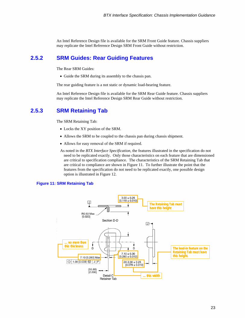
2.5.3 SRM Retaining Tab
The SRM Retaining Tab:
• Locks the XY position of the SRM.
• Allows the SRM to be coupled to the chassis pan during chassis shipment.
• Allows for easy removal of the SRM if required.
As noted in the BTX Interface Specification, the features illustrated in the specification do not need to be replicated exactly. Only those characteristics on each feature that are dimensioned are critical to specification compliance. The characteristics of the SRM Retaining Tab that are critical to compliance are shown in Figure 11. To further illustrate the point that the features from the specification do not need to be replicated exactly, one possible design option is illustrated in Figure 12.
Figure 11: SRM Retaining Tab
The Retaining Tab musthave this height
… this width
… no more thanthis thickness The lead-in feature on the
Retaining Tab must havethis height.
The Retaining Tab musthave this heightThe Retaining Tab musthave this height
… this width… this width
… no more thanthis thickness… no more thanthis thickness The lead-in feature on the
Retaining Tab must havethis height.
The lead-in feature on theRetaining Tab must havethis height.
BTX Interface Specification: Chassis Implementation Guidance
24
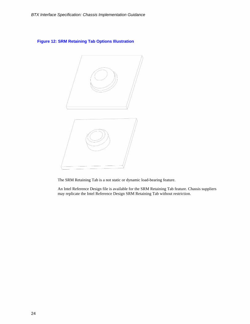
Figure 12: SRM Retaining Tab Options Illustration
The SRM Retaining Tab is a not static or dynamic load-bearing feature.
An Intel Reference Design file is available for the SRM Retaining Tab feature. Chassis suppliers may replicate the Intel Reference Design SRM Retaining Tab without restriction.
BTX Interface Specification: Chassis Implementation Guidance
25
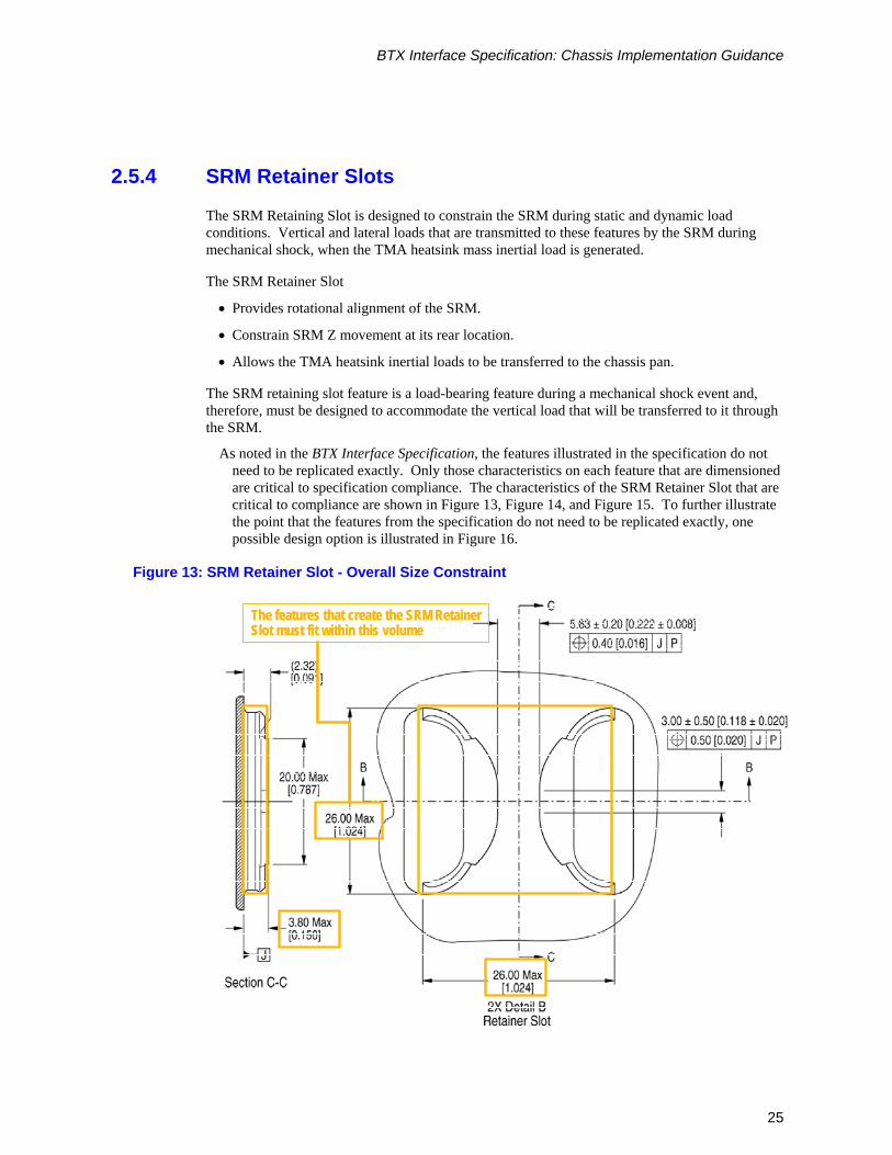
2.5.4 SRM Retainer Slots
The SRM Retaining Slot is designed to constrain the SRM during static and dynamic load conditions. Vertical and lateral loads that are transmitted to these features by the SRM during mechanical shock, when the TMA heatsink mass inertial load is generated.
The SRM Retainer Slot
• Provides rotational alignment of the SRM.
• Constrain SRM Z movement at its rear location.
• Allows the TMA heatsink inertial loads to be transferred to the chassis pan.
The SRM retaining slot feature is a load-bearing feature during a mechanical shock event and, therefore, must be designed to accommodate the vertical load that will be transferred to it through the SRM.
As noted in the BTX Interface Specification, the features illustrated in the specification do not need to be replicated exactly. Only those characteristics on each feature that are dimensioned are critical to specification compliance. The characteristics of the SRM Retainer Slot that are critical to compliance are shown in Figure 13, Figure 14, and Figure 15. To further illustrate the point that the features from the specification do not need to be replicated exactly, one possible design option is illustrated in Figure 16.
Figure 13: SRM Retainer Slot - Overall Size Constraint
The features that create the SRM RetainerSlot must fit within this volumeThe features that create the SRM RetainerSlot must fit within this volumeThe features that create the SRM RetainerSlot must fit within this volume
BTX Interface Specification: Chassis Implementation Guidance
26
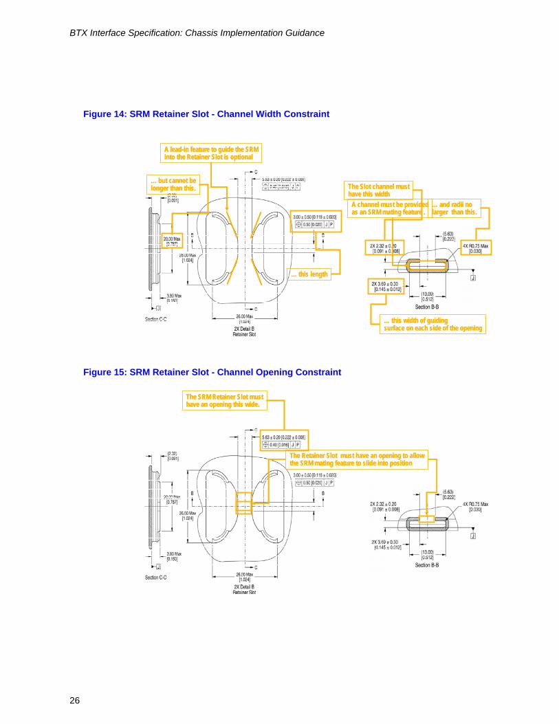
Figure 14: SRM Retainer Slot - Channel Width Constraint
The Slot channel musthave this width
… this length
… this width of guidingsurface on each side of the opening
… and radii nolarger than this.
A channel must be providedas an SRM mating feature .
… but cannot belonger than this.
A lead-in feature to guide the SRMinto the Retainer Slot is optional
The Slot channel musthave this widthThe Slot channel musthave this width
… this length… this length
… this width of guidingsurface on each side of the opening… this width of guidingsurface on each side of the opening
… and radii nolarger than this.… and radii nolarger than this.
A channel must be providedas an SRM mating feature .A channel must be providedas an SRM mating feature .
… but cannot belonger than this.… but cannot belonger than this.
A lead-in feature to guide the SRMinto the Retainer Slot is optionalA lead-in feature to guide the SRMinto the Retainer Slot is optional
Figure 15: SRM Retainer Slot - Channel Opening Constraint
The Retainer Slot must have an opening to allowthe SRM mating feature to slide into position
The SRM Retainer Slot musthave an opening this wide.
The Retainer Slot must have an opening to allowthe SRM mating feature to slide into position The Retainer Slot must have an opening to allowthe SRM mating feature to slide into position
The SRM Retainer Slot musthave an opening this wide.The SRM Retainer Slot musthave an opening this wide.
BTX Interface Specification: Chassis Implementation Guidance
27
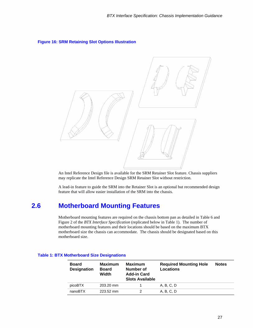
Figure 16: SRM Retaining Slot Options Illustration
An Intel Reference Design file is available for the SRM Retainer Slot feature. Chassis suppliers may replicate the Intel Reference Design SRM Retainer Slot without restriction.
A lead-in feature to guide the SRM into the Retainer Slot is an optional but recommended design feature that will allow easier installation of the SRM into the chassis.
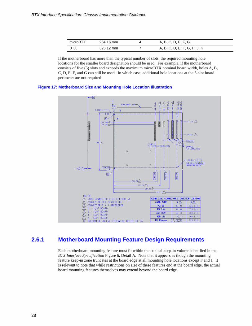
2.6 Motherboard Mounting Features Motherboard mounting features are required on the chassis bottom pan as detailed in Table 6 and Figure 2 of the BTX Interface Specification (replicated below in Table 1). The number of motherboard mounting features and their locations should be based on the maximum BTX motherboard size the chassis can accommodate. The chassis should be designated based on this motherboard size.
Table 1: BTX Motherboard Size Designations
Board Designation
Maximum Board Width
Maximum Number of Add-in Card Slots Available
Required Mounting Hole Locations
Notes
picoBTX 203.20 mm 1 A, B, C, D nanoBTX 223.52 mm 2 A, B, C, D
BTX Interface Specification: Chassis Implementation Guidance
28
microBTX 264.16 mm 4 A, B, C, D, E, F, G BTX 325.12 mm 7 A, B, C, D, E, F, G, H, J, K
If the motherboard has more than the typical number of slots, the required mounting hole locations for the smaller board designation should be used. For example, if the motherboard consists of five (5) slots and exceeds the maximum microBTX nominal board width, holes A, B, C, D, E, F, and G can still be used. In which case, additional hole locations at the 5-slot board perimeter are not required
Figure 17: Motherboard Size and Mounting Hole Location Illustration
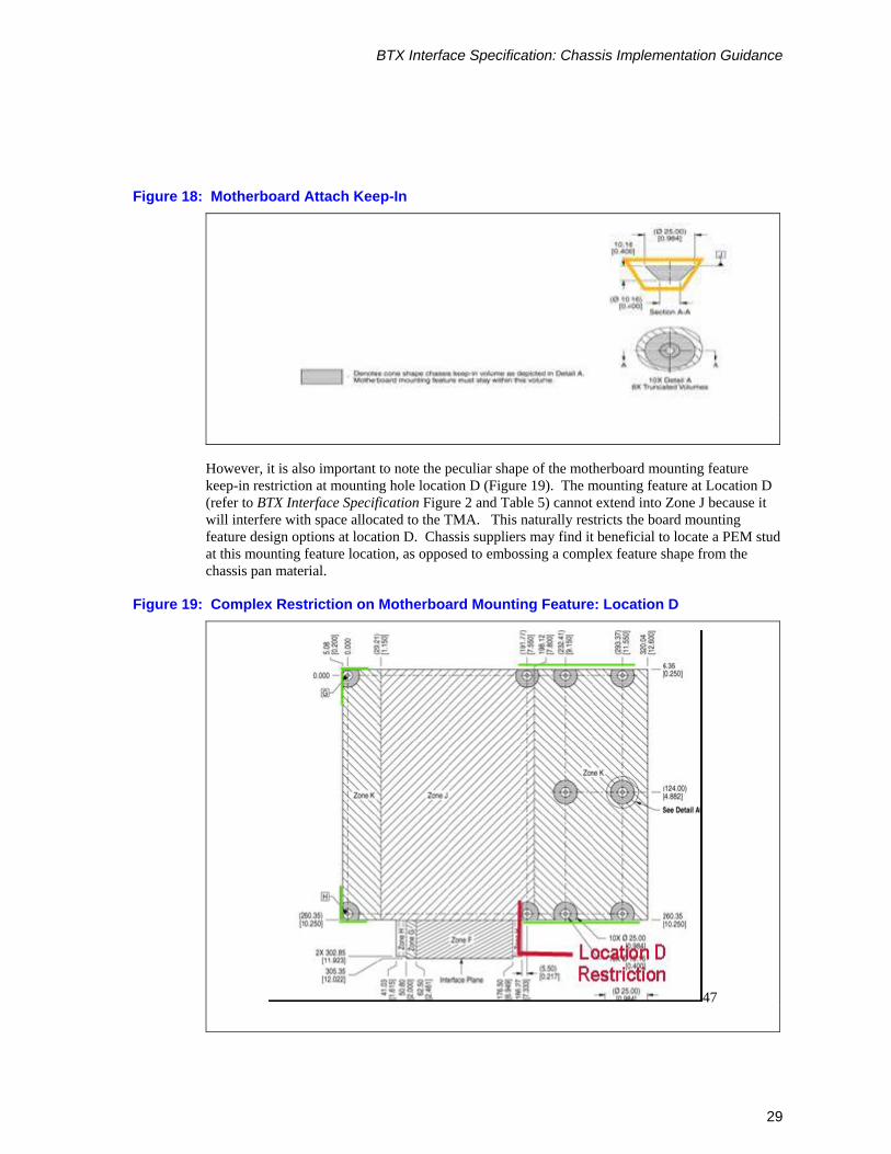
2.6.1 Motherboard Mounting Feature Design Requirements
Each motherboard mounting feature must fit within the conical keep-in volume identified in the BTX Interface Specification Figure 6, Detail A. Note that it appears as though the mounting feature keep-in zone truncates at the board edge at all mounting hole locations except F and J. It is relevant to note that while restrictions on size of these features end at the board edge, the actual board mounting features themselves may extend beyond the board edge.
BTX Interface Specification: Chassis Implementation Guidance
29
Figure 18: Motherboard Attach Keep-In
However, it is also important to note the peculiar shape of the motherboard mounting feature keep-in restriction at mounting hole location D (Figure 19). The mounting feature at Location D (refer to BTX Interface Specification Figure 2 and Table 5) cannot extend into Zone J because it will interfere with space allocated to the TMA. This naturally restricts the board mounting feature design options at location D. Chassis suppliers may find it beneficial to locate a PEM stud at this mounting feature location, as opposed to embossing a complex feature shape from the chassis pan material.
Figure 19: Complex Restriction on Motherboard Mounting Feature: Location D
47
BTX Interface Specification: Chassis Implementation Guidance
30
With the exception noted above, the Motherboard Mounting Feature requirements may be interpreted in the same way as they are interpreted in the ATX Specification and similar design practices can be used for these features.
See Section 2.9.2 for additional structural design recommendations specific to motherboard mounting features.
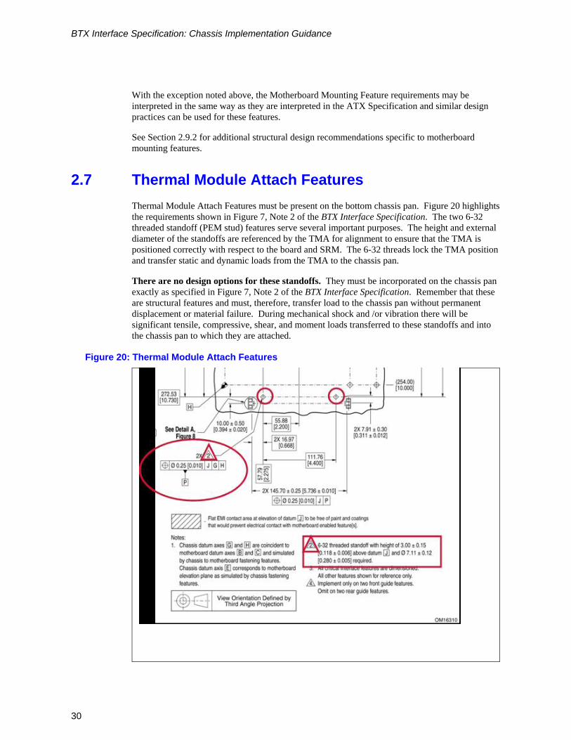
2.7 Thermal Module Attach Features Thermal Module Attach Features must be present on the bottom chassis pan. Figure 20 highlights the requirements shown in Figure 7, Note 2 of the BTX Interface Specification. The two 6-32 threaded standoff (PEM stud) features serve several important purposes. The height and external diameter of the standoffs are referenced by the TMA for alignment to ensure that the TMA is positioned correctly with respect to the board and SRM. The 6-32 threads lock the TMA position and transfer static and dynamic loads from the TMA to the chassis pan.
There are no design options for these standoffs. They must be incorporated on the chassis pan exactly as specified in Figure 7, Note 2 of the BTX Interface Specification. Remember that these are structural features and must, therefore, transfer load to the chassis pan without permanent displacement or material failure. During mechanical shock and /or vibration there will be significant tensile, compressive, shear, and moment loads transferred to these standoffs and into the chassis pan to which they are attached.
Figure 20: Thermal Module Attach Features
BTX Interface Specification: Chassis Implementation Guidance
31
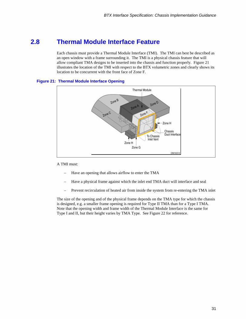
2.8 Thermal Module Interface Feature Each chassis must provide a Thermal Module Interface (TMI). The TMI can best be described as an open window with a frame surrounding it. The TMI is a physical chassis feature that will allow compliant TMA designs to be inserted into the chassis and function properly. Figure 21 illustrates the location of the TMI with respect to the BTX volumetric zones and clearly shows its location to be concurrent with the front face of Zone F.
Figure 21: Thermal Module Interface Opening
A TMI must:
– Have an opening that allows airflow to enter the TMA
– Have a physical frame against which the inlet end TMA duct will interface and seal
– Prevent recirculation of heated air from inside the system from re-entering the TMA inlet
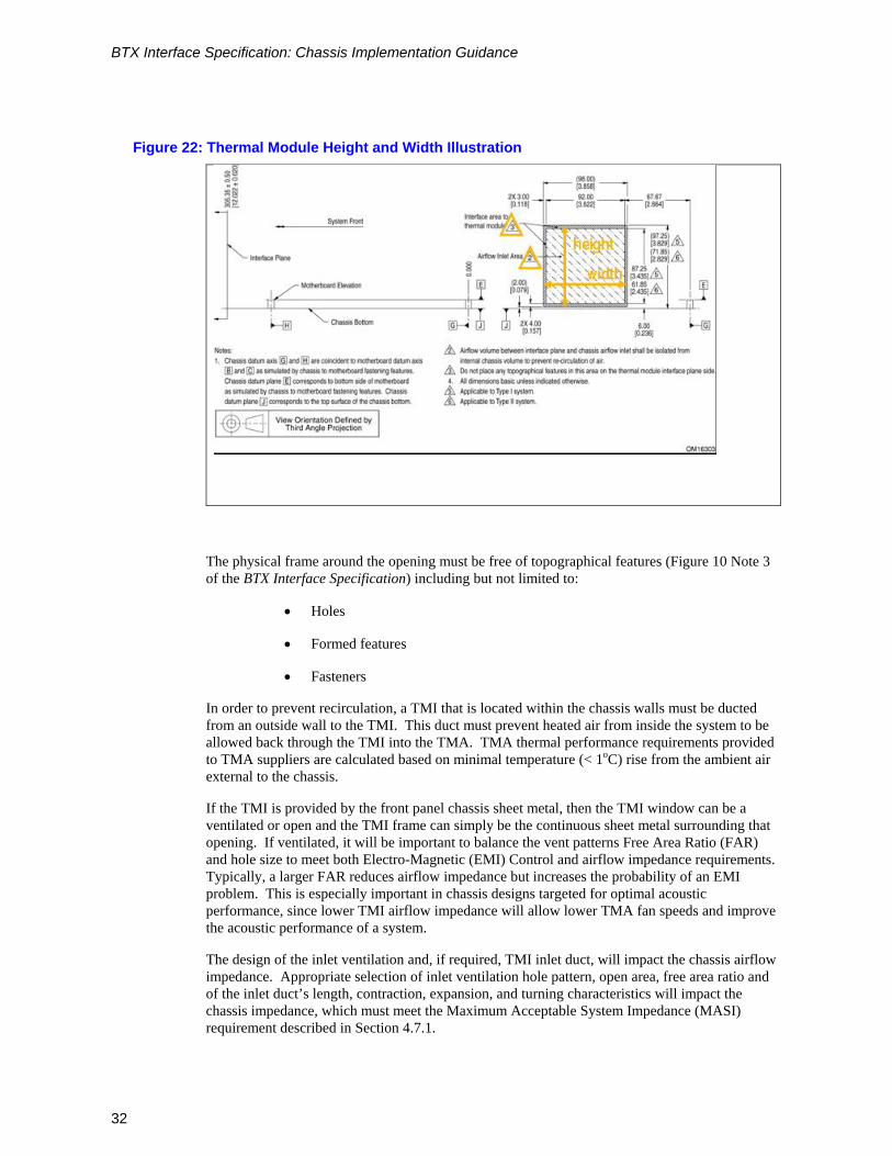
The size of the opening and of the physical frame depends on the TMA type for which the chassis is designed, e.g. a smaller frame opening is required for Type II TMA than for a Type I TMA. Note that the opening width and frame width of the Thermal Module Interface is the same for Type I and II, but their height varies by TMA Type. See Figure 22 for reference.
BTX Interface Specification: Chassis Implementation Guidance
32
Figure 22: Thermal Module Height and Width Illustration
The physical frame around the opening must be free of topographical features (Figure 10 Note 3 of the BTX Interface Specification) including but not limited to:
• Holes
• Formed features
• Fasteners
In order to prevent recirculation, a TMI that is located within the chassis walls must be ducted from an outside wall to the TMI. This duct must prevent heated air from inside the system to be allowed back through the TMI into the TMA. TMA thermal performance requirements provided to TMA suppliers are calculated based on minimal temperature (< 1oC) rise from the ambient air external to the chassis.
If the TMI is provided by the front panel chassis sheet metal, then the TMI window can be a ventilated or open and the TMI frame can simply be the continuous sheet metal surrounding that opening. If ventilated, it will be important to balance the vent patterns Free Area Ratio (FAR) and hole size to meet both Electro-Magnetic (EMI) Control and airflow impedance requirements. Typically, a larger FAR reduces airflow impedance but increases the probability of an EMI problem. This is especially important in chassis designs targeted for optimal acoustic performance, since lower TMI airflow impedance will allow lower TMA fan speeds and improve the acoustic performance of a system.
The design of the inlet ventilation and, if required, TMI inlet duct, will impact the chassis airflow impedance. Appropriate selection of inlet ventilation hole pattern, open area, free area ratio and of the inlet duct’s length, contraction, expansion, and turning characteristics will impact the chassis impedance, which must meet the Maximum Acceptable System Impedance (MASI) requirement described in Section 4.7.1.
BTX Interface Specification: Chassis Implementation Guidance
33
2.8.1 Thermal Module Interface Ducting Alternatives
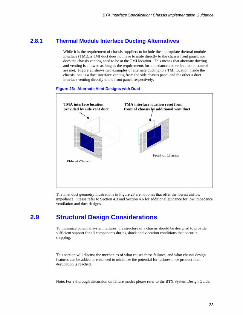
While it is the requirement of chassis suppliers to include the appropriate thermal module interface (TMI), a TMI duct does not have to mate directly to the chassis front panel, nor does the chassis venting need to be at the TMI location. This means that alternate ducting and venting is allowed as long as the requirements for impedance and recirculation control are met. Figure 23 shows two examples of alternate ducting to a TMI location inside the chassis; one is a duct interface venting from the side chassis panel and the other a duct interface venting directly to the front panel, respectively.
Figure 23: Alternate Vent Designs with Duct
The inlet duct geometry illustrations in Figure 23 are not ones that offer the lowest airflow impedance. Please refer to Section 4.3 and Section 4.6 for additional guidance for low impedance ventilation and duct designs.
2.9 Structural Design Considerations To minimize potential system failures, the structure of a chassis should be designed to provide sufficient support for all components during shock and vibration conditions that occur in shipping.
This section will discuss the mechanics of what causes these failures, and what chassis design features can be added or enhanced to minimize the potential for failures once product final destination is reached..
Note: For a thorough discussion on failure modes please refer to the BTX System Design Guide.
TMA interface location provided by side vent duct
TMA interface location reset from front of chassis by additional vent duct
Side of ChassisFront of Chassis
BTX Interface Specification: Chassis Implementation Guidance
34
2.9.1 Design Considerations for Failure Modes
There are several important structural chassis design features and each are tied to the inner pan construction, and each can have differing influences to component failure modes.
Excessive Deflection -- A failure as a result of excessive deflection exists when motherboard/components move excessively with respect to the chassis and either contact other components, become dislodge from their mountings, or damage internal to the component occurs. This generally occurs when the overall pan stiffness or board mounting is insufficient.
Plastic Deformation -- Plastic deformation occurs when the chassis is deformed beyond the elastic region and permanent deformation occurs such that the chassis fails to perform as it did prior to the deformation. This allows excessive free movement of the chassis pan that was not initially present. This occurs when insufficient provisions for yielding and inadequate material properties are combined
Stress Concentration -- Failure in this mode is a result of a tight bend radius at a key location. This condition occurs when chassis pan stiffening does not span the required distance necessary to spread the load.
The BTX chassis incorporates a Support and Retention Module (SRM) to provide support and reduce flexure of the motherboard to aid in minimizing the solder ball failure mode. However, additional stiffness is necessary in the chassis to guard against solder ball failure. The following section discusses solder ball failures.
2.9.1.1 Solder Ball Failure Modes
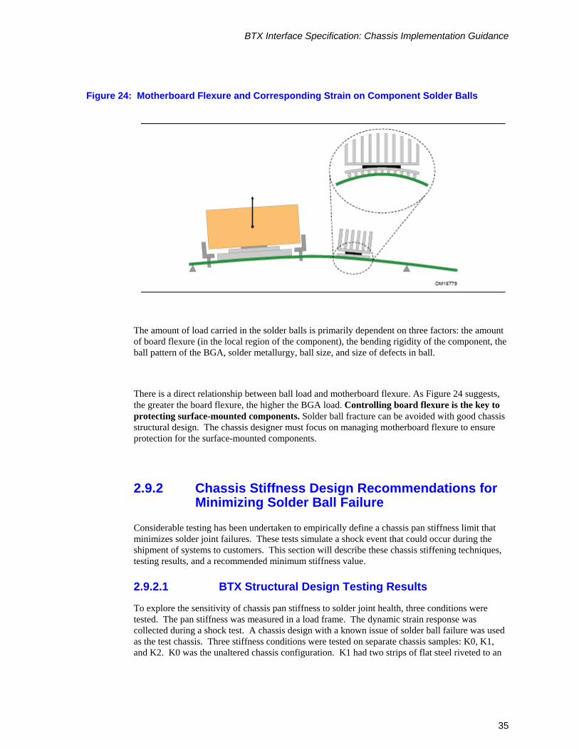
Solder ball cracking and fracture is a failure mode associated with motherboard flexure. Surface-mounted components (such as the CPU socket, ICH, or MCH) can experience this type of failure. During dynamic events such as a dropped package during shipping where the motherboard is subjected to severe bending, these surface-mount components develop tensile, compressive, and shear stresses within each solder ball in the BGA. Especially susceptible are the corner balls of the array. In a shock condition, the inertial loads act to flex the motherboard (see Figure 24). This generates curvature throughout the board, including the area under the surface-mounted component. The component (which is stiffer that the board) will resist flexing with the board, thereby generating higher loads at the interface between the board and component.
BTX Interface Specification: Chassis Implementation Guidance
35
Figure 24: Motherboard Flexure and Corresponding Strain on Component Solder Balls
The amount of load carried in the solder balls is primarily dependent on three factors: the amount of board flexure (in the local region of the component), the bending rigidity of the component, the ball pattern of the BGA, solder metallurgy, ball size, and size of defects in ball.
There is a direct relationship between ball load and motherboard flexure. As Figure 24 suggests, the greater the board flexure, the higher the BGA load. Controlling board flexure is the key to protecting surface-mounted components. Solder ball fracture can be avoided with good chassis structural design. The chassis designer must focus on managing motherboard flexure to ensure protection for the surface-mounted components.
2.9.2 Chassis Stiffness Design Recommendations for Minimizing Solder Ball Failure
Considerable testing has been undertaken to empirically define a chassis pan stiffness limit that minimizes solder joint failures. These tests simulate a shock event that could occur during the shipment of systems to customers. This section will describe these chassis stiffening techniques, testing results, and a recommended minimum stiffness value.
2.9.2.1 BTX Structural Design Testing Results
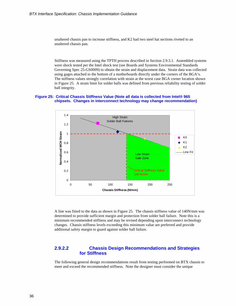
To explore the sensitivity of chassis pan stiffness to solder joint health, three conditions were tested. The pan stiffness was measured in a load frame. The dynamic strain response was collected during a shock test. A chassis design with a known issue of solder ball failure was used as the test chassis. Three stiffness conditions were tested on separate chassis samples: K0, K1, and K2. K0 was the unaltered chassis configuration. K1 had two strips of flat steel riveted to an
BTX Interface Specification: Chassis Implementation Guidance
36
unaltered chassis pan to increase stiffness, and K2 had two steel hat sections riveted to an unaltered chassis pan.
Stiffness was measured using the TPTH process described in Section 2.9.3.1. Assembled systems were shock tested per the Intel shock test (see Boards and Systems Environmental Standards Governing Spec 25-GS0009) to obtain the strain and displacement data. Strain data was collected using gages attached to the bottom of a motherboards directly under the corners of the BGA’s. The stiffness values strongly correlation with strain at the worst case BGA corner location shown in Figure 25. A strain limit for solder balls was defined from previous reliability testing of solder ball integrity.
Figure 25: Critical Chassis Stiffness Value (Note all data is collected from Intel® 965 chipsets. Changes in interconnect technology may change recommendation)
0
0.2
0.4
0.6
0.8
1
1.2
1.4
0 50 100 150 200 250
Chassis Stiffness (N/mm)
Nor
mal
ized
MCH
Stra
in
K0K1K2Line Fit
High StrainSolder Ball Failures
Low StrainSafe Zone
Critical Stiffness Value140 N/mm
A line was fitted to the data as shown in Figure 25. The chassis stiffness value of 140N/mm was determined to provide sufficient margin and protection from solder ball failure. Note this is a minimum recommended stiffness and may be revised depending upon interconnect technology changes. Chassis stiffness levels exceeding this minimum value are preferred and provide additional safety margin to guard against solder ball failure.
2.9.2.2 Chassis Design Recommendations and Strategies for Stiffness
The following general design recommendations result from testing performed on BTX chassis to meet and exceed the recommended stiffness. Note the designer must consider the unique
BTX Interface Specification: Chassis Implementation Guidance
37
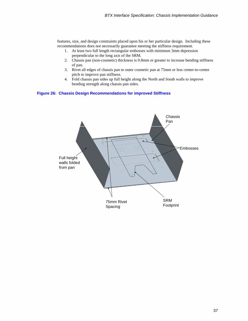
features, size, and design constraints placed upon his or her particular design. Including these recommendations does not necessarily guarantee meeting the stiffness requirement.
1. At least two full length rectangular embosses with minimum 3mm depression perpendicular to the long axis of the SRM.
2. Chassis pan (non-cosmetic) thickness is 0.8mm or greater to increase bending stiffness of pan.
3. Rivet all edges of chassis pan to outer cosmetic pan at 75mm or less center-to-center pitch to improve pan stiffness.
4. Fold chassis pan sides up full height along the North and South walls to improve bending strength along chassis pan sides.
Figure 26: Chassis Design Recommendations for improved Stiffness
SRM Footprint
Chassis Pan
75mm Rivet Spacing
Full height walls folded from pan
Embosses
BTX Interface Specification: Chassis Implementation Guidance
38
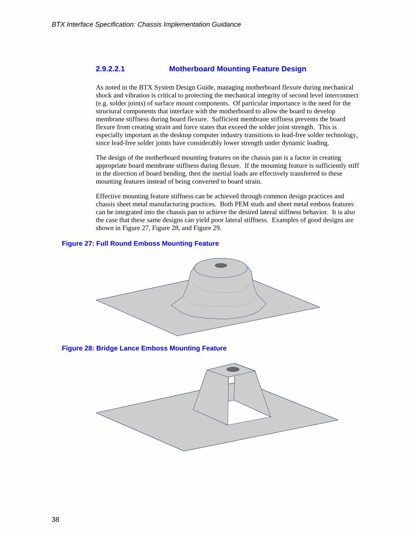
2.9.2.2.1 Motherboard Mounting Feature Design
As noted in the BTX System Design Guide, managing motherboard flexure during mechanical shock and vibration is critical to protecting the mechanical integrity of second level interconnect (e.g. solder joints) of surface mount components. Of particular importance is the need for the structural components that interface with the motherboard to allow the board to develop membrane stiffness during board flexure. Sufficient membrane stiffness prevents the board flexure from creating strain and force states that exceed the solder joint strength. This is especially important as the desktop computer industry transitions to lead-free solder technology, since lead-free solder joints have considerably lower strength under dynamic loading.
The design of the motherboard mounting features on the chassis pan is a factor in creating appropriate board membrane stiffness during flexure. If the mounting feature is sufficiently stiff in the direction of board bending, then the inertial loads are effectively transferred to these mounting features instead of being converted to board strain.
Effective mounting feature stiffness can be achieved through common design practices and chassis sheet metal manufacturing practices. Both PEM studs and sheet metal emboss features can be integrated into the chassis pan to achieve the desired lateral stiffness behavior. It is also the case that these same designs can yield poor lateral stiffness. Examples of good designs are shown in Figure 27, Figure 28, and Figure 29.
Figure 27: Full Round Emboss Mounting Feature
Figure 28: Bridge Lance Emboss Mounting Feature
BTX Interface Specification: Chassis Implementation Guidance
39
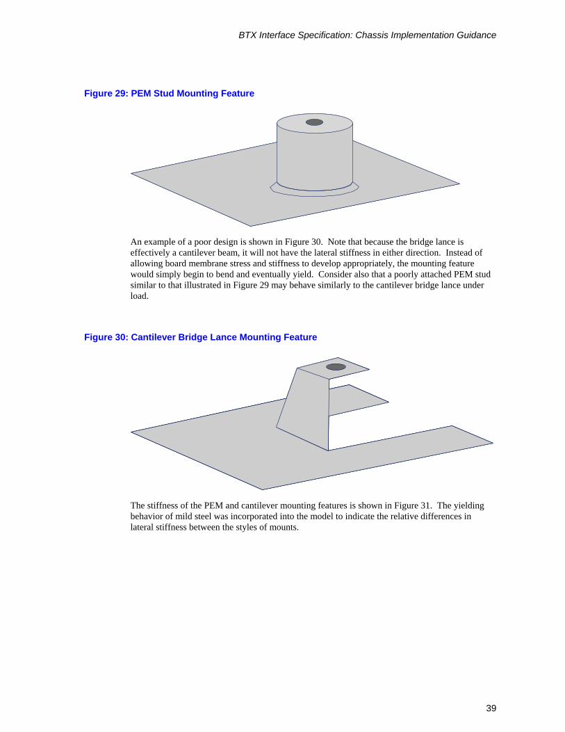
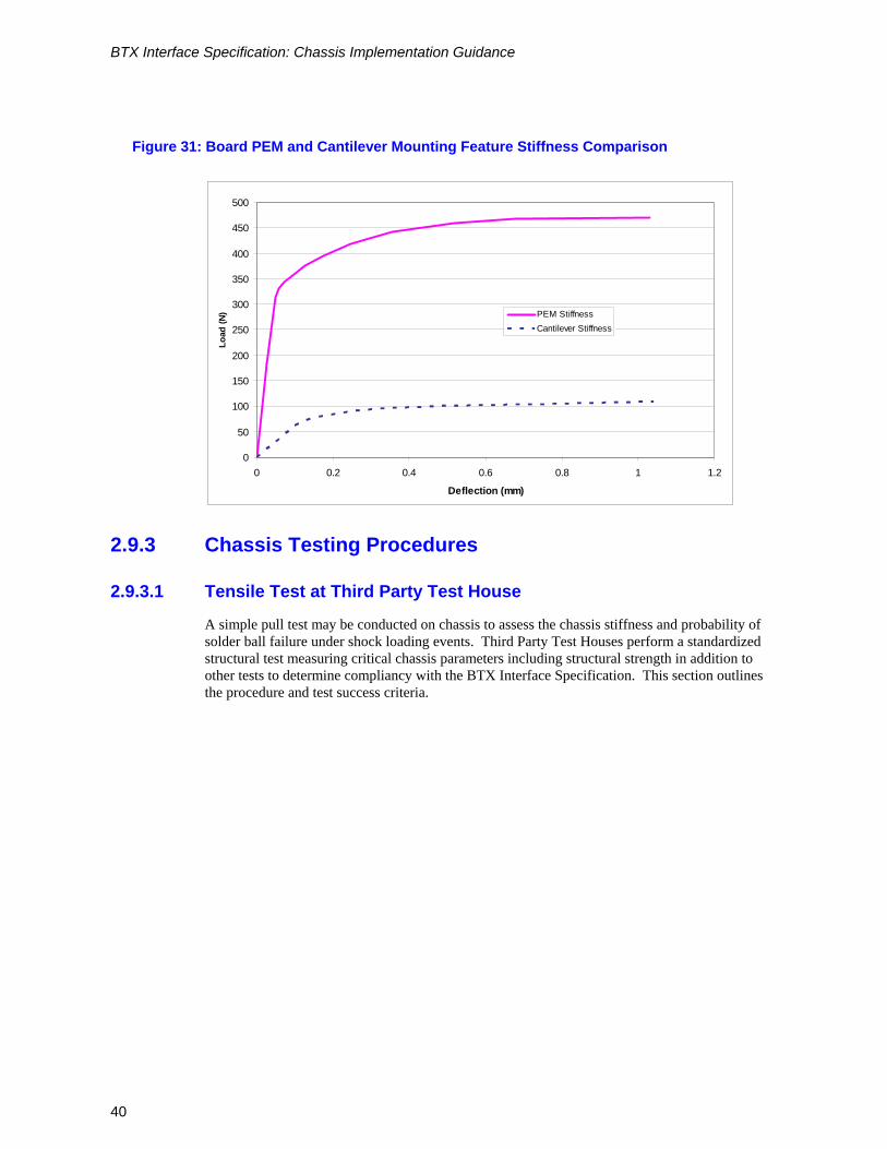
Figure 29: PEM Stud Mounting Feature
An example of a poor design is shown in Figure 30. Note that because the bridge lance is effectively a cantilever beam, it will not have the lateral stiffness in either direction. Instead of allowing board membrane stress and stiffness to develop appropriately, the mounting feature would simply begin to bend and eventually yield. Consider also that a poorly attached PEM stud similar to that illustrated in Figure 29 may behave similarly to the cantilever bridge lance under load.
Figure 30: Cantilever Bridge Lance Mounting Feature
The stiffness of the PEM and cantilever mounting features is shown in Figure 31. The yielding behavior of mild steel was incorporated into the model to indicate the relative differences in lateral stiffness between the styles of mounts.
BTX Interface Specification: Chassis Implementation Guidance
40
Figure 31: Board PEM and Cantilever Mounting Feature Stiffness Comparison
0
50
100
150
200
250
300
350
400
450
500
0 0.2 0.4 0.6 0.8 1 1.2
Deflection (mm)
Load
(N) PEM Stiffness
Cantilever Stiffness
2.9.3 Chassis Testing Procedures
2.9.3.1 Tensile Test at Third Party Test House
A simple pull test may be conducted on chassis to assess the chassis stiffness and probability of solder ball failure under shock loading events. Third Party Test Houses perform a standardized structural test measuring critical chassis parameters including structural strength in addition to other tests to determine compliancy with the BTX Interface Specification. This section outlines the procedure and test success criteria.
BTX Interface Specification: Chassis Implementation Guidance
41
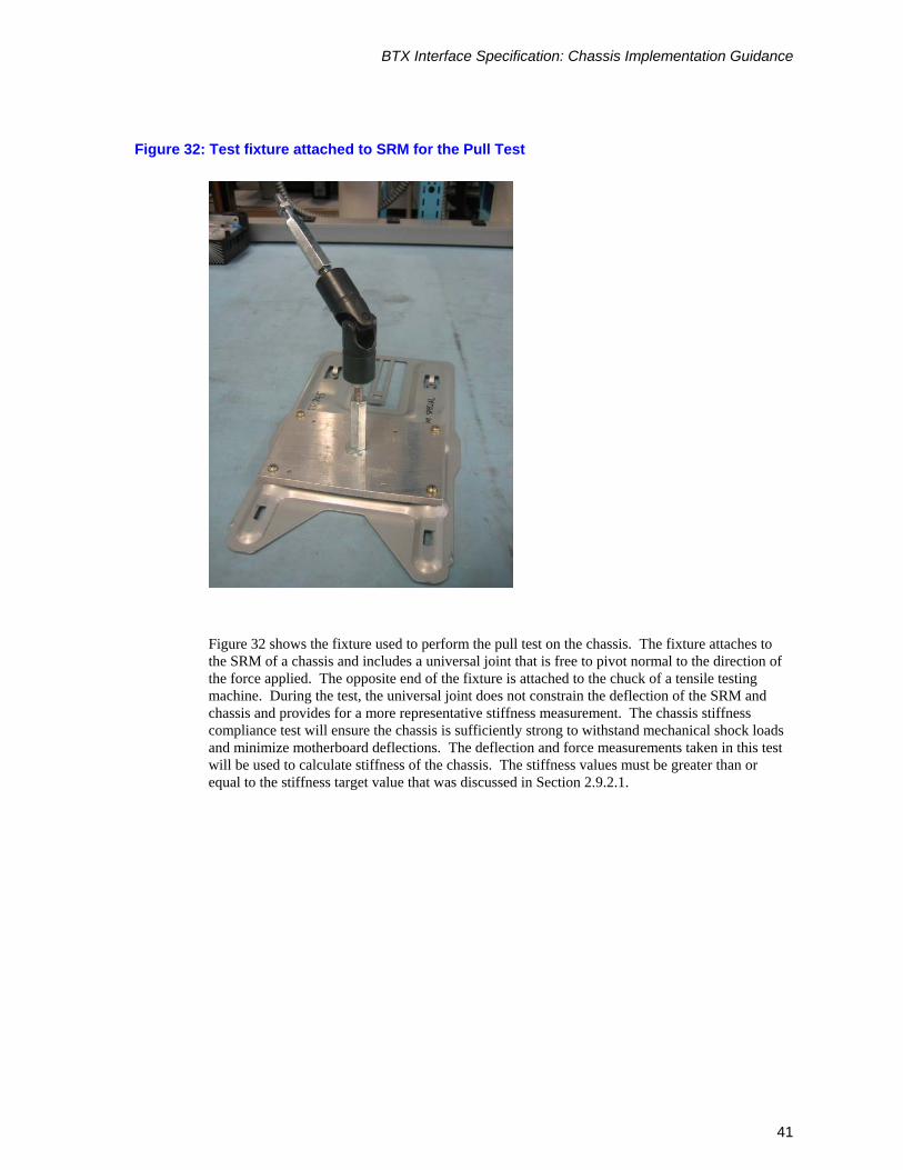
Figure 32: Test fixture attached to SRM for the Pull Test
Figure 32 shows the fixture used to perform the pull test on the chassis. The fixture attaches to the SRM of a chassis and includes a universal joint that is free to pivot normal to the direction of the force applied. The opposite end of the fixture is attached to the chuck of a tensile testing machine. During the test, the universal joint does not constrain the deflection of the SRM and chassis and provides for a more representative stiffness measurement. The chassis stiffness compliance test will ensure the chassis is sufficiently strong to withstand mechanical shock loads and minimize motherboard deflections. The deflection and force measurements taken in this test will be used to calculate stiffness of the chassis. The stiffness values must be greater than or equal to the stiffness target value that was discussed in Section 2.9.2.1.
BTX Interface Specification: Chassis Implementation Guidance
42
< This page is left intentionally blank >
Rear Panel Design Considerations
43
3 Rear Panel Design Considerations
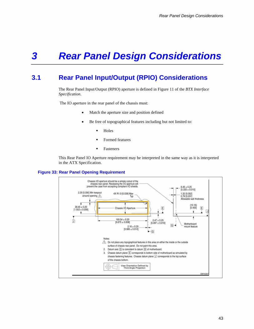
3.1 Rear Panel Input/Output (RPIO) Considerations The Rear Panel Input/Output (RPIO) aperture is defined in Figure 11 of the BTX Interface Specification.
The IO aperture in the rear panel of the chassis must:
• Match the aperture size and position defined
• Be free of topographical features including but not limited to:
Holes
Formed features
Fasteners
This Rear Panel IO Aperture requirement may be interpreted in the same way as it is interpreted in the ATX Specification.
Figure 33: Rear Panel Opening Requirement
Rear Panel Design Considerations
44
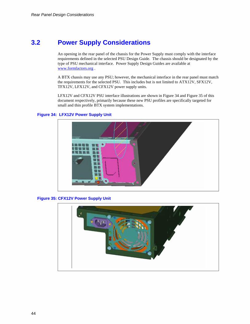
3.2 Power Supply Considerations An opening in the rear panel of the chassis for the Power Supply must comply with the interface requirements defined in the selected PSU Design Guide. The chassis should be designated by the type of PSU mechanical interface. Power Supply Design Guides are available at www.formfactors.org .
A BTX chassis may use any PSU; however, the mechanical interface in the rear panel must match the requirements for the selected PSU. This includes but is not limited to ATX12V, SFX12V, TFX12V, LFX12V, and CFX12V power supply units.
LFX12V and CFX12V PSU interface illustrations are shown in Figure 34 and Figure 35 of this document respectively, primarily because these new PSU profiles are specifically targeted for small and thin profile BTX system implementations.
Figure 34: LFX12V Power Supply Unit
Figure 35: CFX12V Power Supply Unit
Rear Panel Design Considerations
45
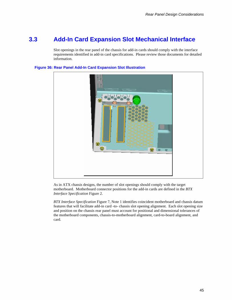
3.3 Add-In Card Expansion Slot Mechanical Interface Slot openings in the rear panel of the chassis for add-in cards should comply with the interface requirements identified in add-in card specifications. Please review those documents for detailed information.
Figure 36: Rear Panel Add-In Card Expansion Slot Illustration
As in ATX chassis designs, the number of slot openings should comply with the target motherboard. Motherboard connector positions for the add-in cards are defined in the BTX Interface Specification Figure 2.
BTX Interface Specification Figure 7, Note 1 identifies coincident motherboard and chassis datum features that will facilitate add-in card -to- chassis slot opening alignment. Each slot opening size and position on the chassis rear panel must account for positional and dimensional tolerances of the motherboard components, chassis-to-motherboard alignment, card-to-board alignment, and card.
Rear Panel Design Considerations
46
3.4 Structural Design Considerations
3.4.1 Rear Panel Sheet Metal Thickness
The rear panel has special structural design considerations.
The PSU is typically attached directly to the rear panel. In mechanical shock, the accelerated mass of the PSU will certainly transfer considerable bending and shear load the rear panel attach features, which the rear panel sheet metal must accommodate without yielding.
Because it is also typical to extensively perforate the rear panel to accommodate exhaust airflow ventilation, add-in card openings, and rear panel I/O, the structural integrity of the rear panel sheet metal is significantly compromised. Yielding and buckling are two common failures modes for rear panel sheet metal that the chassis supplier must consider.
Intel recommends that the chassis use a minimum 0.8-1.0mm sheet metal for the rear panel and that the rear panel be made from the same continuous section of sheet metal used to form the chassis pan and all the chassis pan features (see Sections 2.5, 2.6, and 2.7). The additional stiffness offered by bending the chassis pan sheet metal to form the rear panel will improve the chassis pan and rear panel structural integrity.
Chassis Vent Design
47
4 Chassis Vent Design Chassis vent design plays an important role in the system impedance characteristics, which affect the system’s thermal and acoustic performance. The BTX System Design Guide has detailed information on venting guidelines and recommendations. In addition, the BTX System Design Guide has the necessary and applicable equations needed to calculate vent impedance losses.
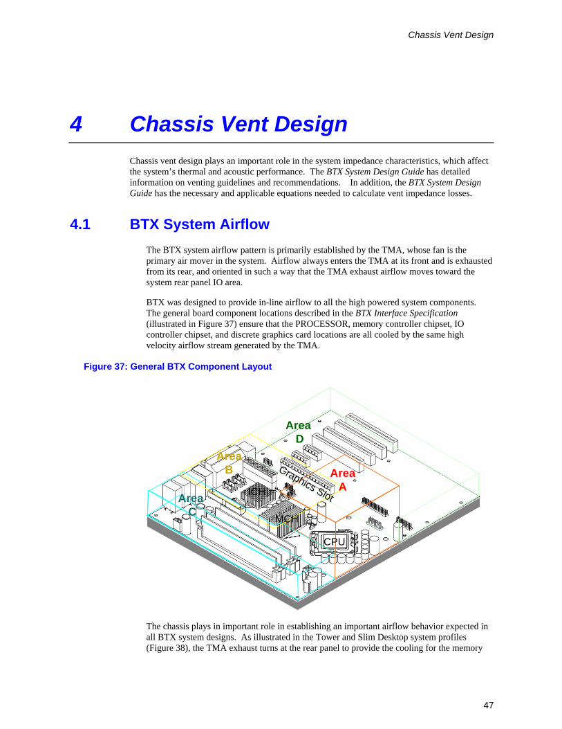
4.1 BTX System Airflow The BTX system airflow pattern is primarily established by the TMA, whose fan is the primary air mover in the system. Airflow always enters the TMA at its front and is exhausted from its rear, and oriented in such a way that the TMA exhaust airflow moves toward the system rear panel IO area.
BTX was designed to provide in-line airflow to all the high powered system components. The general board component locations described in the BTX Interface Specification (illustrated in Figure 37) ensure that the PROCESSOR, memory controller chipset, IO controller chipset, and discrete graphics card locations are all cooled by the same high velocity airflow stream generated by the TMA.
Figure 37: General BTX Component Layout
Area B
Area D
Area A
Area C
CPU
MCH
Graphics SlotICH
Area B
Area D
Area A
Area C
CPU
MCH
Graphics SlotICH
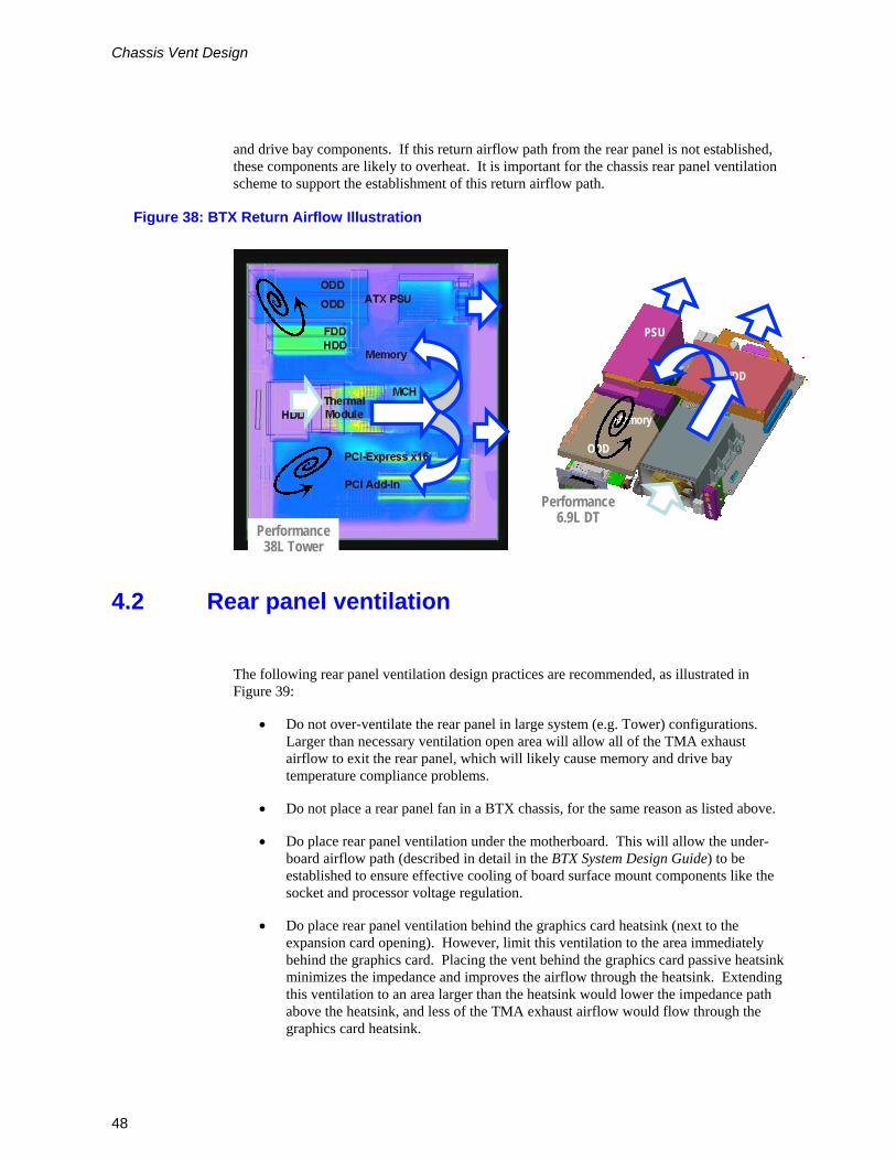
The chassis plays in important role in establishing an important airflow behavior expected in all BTX system designs. As illustrated in the Tower and Slim Desktop system profiles (Figure 38), the TMA exhaust turns at the rear panel to provide the cooling for the memory
Chassis Vent Design
48
and drive bay components. If this return airflow path from the rear panel is not established, these components are likely to overheat. It is important for the chassis rear panel ventilation scheme to support the establishment of this return airflow path.
Figure 38: BTX Return Airflow Illustration
Performance38L Tower
ODD
HDD
PSU
Memory
Performance6.9L DT
Performance38L Tower
ODD
HDD
PSU
Memory
Performance6.9L DT
4.2 Rear panel ventilation
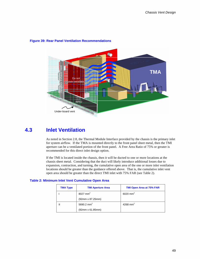
The following rear panel ventilation design practices are recommended, as illustrated in Figure 39:
• Do not over-ventilate the rear panel in large system (e.g. Tower) configurations. Larger than necessary ventilation open area will allow all of the TMA exhaust airflow to exit the rear panel, which will likely cause memory and drive bay temperature compliance problems.
• Do not place a rear panel fan in a BTX chassis, for the same reason as listed above.
• Do place rear panel ventilation under the motherboard. This will allow the under-board airflow path (described in detail in the BTX System Design Guide) to be established to ensure effective cooling of board surface mount components like the socket and processor voltage regulation.
• Do place rear panel ventilation behind the graphics card heatsink (next to the expansion card opening). However, limit this ventilation to the area immediately behind the graphics card. Placing the vent behind the graphics card passive heatsink minimizes the impedance and improves the airflow through the heatsink. Extending this ventilation to an area larger than the heatsink would lower the impedance path above the heatsink, and less of the TMA exhaust airflow would flow through the graphics card heatsink.
Chassis Vent Design
49
Figure 39: Rear Panel Ventilation Recommendations
TMADo not
over-ventilate
RPIO
Gra
phic
s E
xhau
st V
ent
Under-board vent
TMATMADo not
over-ventilate
RPIO
Gra
phic
s E
xhau
st V
ent
Under-board vent
4.3 Inlet Ventilation As noted in Section 2.8, the Thermal Module Interface provided by the chassis is the primary inlet for system airflow. If the TMA is mounted directly to the front panel sheet metal, then the TMI aperture can be a ventilated portion of the front panel. A Free Area Ratio of 75% or greater is recommended for this direct inlet design option.
If the TMI is located inside the chassis, then it will be ducted to one or more locations at the chassis sheet metal. Considering that the duct will likely introduce additional losses due to expansion, contraction, and turning, the cumulative open area of the one or more inlet ventilation locations should be greater than the guidance offered above. That is, the cumulative inlet vent open area should be greater than the direct TMI inlet with 75% FAR (see Table 2).
Table 2: Minimum Inlet Vent Cumulative Open Area
TMA Type TMI Aperture Area TMI Open Area at 75% FAR
I 8027 mm2
(92mm x 87.25mm)
6020 mm2
II 5690.2 mm2
(92mm x 61.85mm)
4268 mm2
Chassis Vent Design
50
4.4 Inlet Vent Filter Guidance The BTX Interface Specification does not require an air filter at the TMI inlet, which are usually integrated to minimize dust contamination inside the system. Because filters will increase the airflow impedance, they can be expected to degrade the thermal and /or acoustic performance. If the filter impedance is not compensated for by an increase in TMA fan speed or a reduction in the impedance characteristic of another part of the chassis design, then the system may not be able to meet all the system’s component temperature specifications. On the other hand, the higher TMA fan speed required to overcome the filter’s impedance and meet the component temperature specifications will likely increase the system’s noise. If a filter is included in the chassis design, Intel recommends that the integrator document and distribute end user filter maintenance requirements.
4.5 Exhaust Ventilation As noted in Section 4.1 and Figure 38, properly designed BTX systems will usually have a return airflow path from the rear panel. Rear panel exhaust ventilation design recommendations are outlined in Section 4.2. It is, of course, also important to provide an exhaust path for the return airflow from the rear panel.
The return airflow is primarily responsible for cooling the memory and drive bay components, though there are systems configurations in which the drive components (i.e. HDD) can be cooled by the direct TMA exhaust flow if these are placed between the rear panel and TMA. More common system configurations will place the drive bay components near the front of the system, on either side or above the TMA.
Exhaust ventilation near these drive bay components is critical to ensuring adequate cooling; without proper ventilation, the return airflow will accumulate and stagnate in the drive bay area and lead to temperature compliance problems. If side or top panel ventilation is tolerable from an industrial design and regulatory perspective, these vent locations will provide a reasonable exhaust flow path sufficient to keep the drive bays within their temperature specifications. Front panel exhaust ventilation for the drive bays will often be less effective but can be sufficient if the total open area prevents stagnation. Special considerations for the front bezel design are required if front panel exhaust ventilation is used – see Section 4.6.
4.6 Front Bezel
4.6.1 Inlet Ventilation
A chassis designer is often also responsible for the design of the front bezel. Design options are illustrated in the BTX System Design Guide that shows several bezel airflow inlet vent locations and “blinded” ventilation design options for the front face. Although it is acoustically optimal to have the lowest possible vent and channel impedance through the bezel, a large opening immediately in front of the TMI is not always an attractive industrial design option. Fundamentally, the impedance of the bezel will be higher:
– as the total inlet vent area is decreased
Chassis Vent Design
51
– as the Free Area Ratio of the inlet vent is decreased
– as the number of turns is increased (turning loss)
– if the duct cross-sectional area increases (expansion loss) or decreases (contraction loss)
– as the duct length increases (channel loss)
Ventilation of the front bezel is not required as there are certainly inlet ventilation options on other chassis panels than the front panel. However, bezel ventilation is typically beneficial since it typically allows the airflow to enter the TMA through the front panel with the lowest possible total impedance.
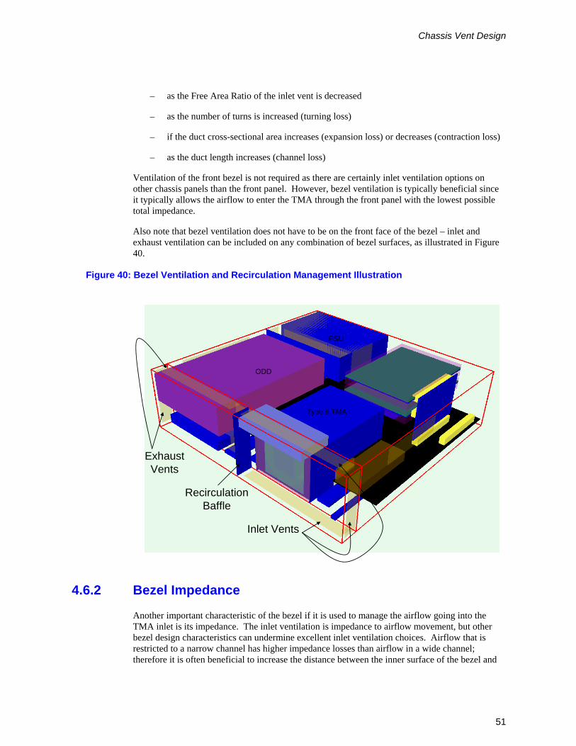
Also note that bezel ventilation does not have to be on the front face of the bezel – inlet and exhaust ventilation can be included on any combination of bezel surfaces, as illustrated in Figure 40.
Figure 40: Bezel Ventilation and Recirculation Management Illustration
ODD
PSU
Type II TMA
ExhaustVents
RecirculationBaffle
Inlet Vents
ODD
PSU
Type II TMA
ExhaustVents
RecirculationBaffle
Inlet Vents
4.6.2 Bezel Impedance
Another important characteristic of the bezel if it is used to manage the airflow going into the TMA inlet is its impedance. The inlet ventilation is impedance to airflow movement, but other bezel design characteristics can undermine excellent inlet ventilation choices. Airflow that is restricted to a narrow channel has higher impedance losses than airflow in a wide channel; therefore it is often beneficial to increase the distance between the inner surface of the bezel and
Chassis Vent Design
52
the front panel sheet metal. Sudden increases or decreases in the cross-section of the channel through which the airflow moves is also an impedance, so it is best if the bezel’s airflow channel is a reasonably constant cross-section from the bezel inlet to the TMA inlet. Finally, there is impedance introduced when airflow has to turn suddenly. If the bezel inlet and TMA inlet are not in-line, then any turns designed into the bezel (or, for that matter, any duct that may extend from the sheet metal to the TMA inlet) should use gradual turns to smoothly transition the airflow direction.
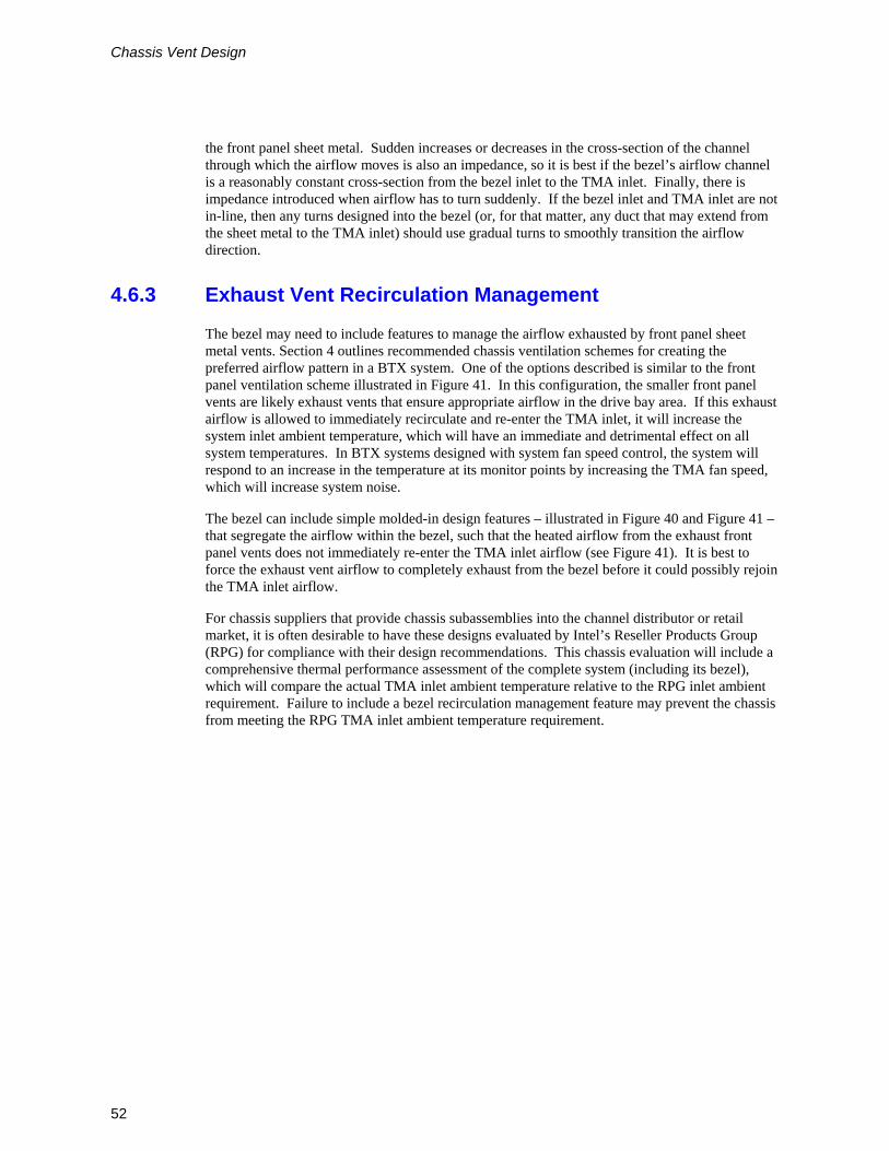
4.6.3 Exhaust Vent Recirculation Management
The bezel may need to include features to manage the airflow exhausted by front panel sheet metal vents. Section 4 outlines recommended chassis ventilation schemes for creating the preferred airflow pattern in a BTX system. One of the options described is similar to the front panel ventilation scheme illustrated in Figure 41. In this configuration, the smaller front panel vents are likely exhaust vents that ensure appropriate airflow in the drive bay area. If this exhaust airflow is allowed to immediately recirculate and re-enter the TMA inlet, it will increase the system inlet ambient temperature, which will have an immediate and detrimental effect on all system temperatures. In BTX systems designed with system fan speed control, the system will respond to an increase in the temperature at its monitor points by increasing the TMA fan speed, which will increase system noise.
The bezel can include simple molded-in design features – illustrated in Figure 40 and Figure 41 – that segregate the airflow within the bezel, such that the heated airflow from the exhaust front panel vents does not immediately re-enter the TMA inlet airflow (see Figure 41). It is best to force the exhaust vent airflow to completely exhaust from the bezel before it could possibly rejoin the TMA inlet airflow.
For chassis suppliers that provide chassis subassemblies into the channel distributor or retail market, it is often desirable to have these designs evaluated by Intel’s Reseller Products Group (RPG) for compliance with their design recommendations. This chassis evaluation will include a comprehensive thermal performance assessment of the complete system (including its bezel), which will compare the actual TMA inlet ambient temperature relative to the RPG inlet ambient requirement. Failure to include a bezel recirculation management feature may prevent the chassis from meeting the RPG TMA inlet ambient temperature requirement.
Chassis Vent Design
53
Figure 41: Bezel Recirculation Management Feature
OM16748
BezelPartition
BezelInlet Vent
Bezel Exhaust Vent
Thermal ModuleInterface
Front PanelVents
4.7 Chassis Impedance Chassis impedance is a measure of its resistance to airflow movement. Many design characteristics of the chassis contribute to the total chassis impedance: inlet and exhaust ventilation, bezel inlet, bezel depth, and the duct to the TMI. The TMA generates the system airflow and guidelines for the TMA effective fan curve, which is a measure of the TMA fan’s ability to move airflow against impedance, are defined in the TMA EDRD.
By assuring the each BTX chassis meets the Maximum Acceptable System Impedance (MASI) criteria, system integrators are assured that the use of compliant TMAs will result in acceptable system airflow and component cooling.
It is anticipated that the systems into which Type I Vs Type II TMA designs are integrated will be considerably different from one another (e.g. systems that use a Type II TMA are likely to be thinner than those that use Type I) Therefore, the MASI is different for Type I Vs Type II chassis designs (designated, MASI_I and MASI_II, respectively), as are the effective fan curve guidelines for Type I and Type II TMA designs.
4.7.1 Maximum Acceptable System Impedance
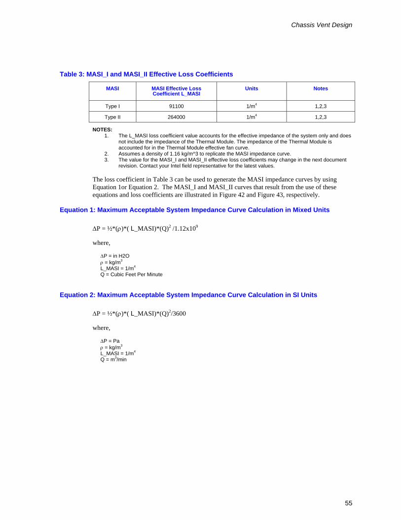
Table 3 shows the loss coefficients for the MASI_I and MASI_II requirements curves. These values can be used by suppliers to compare impedance curves during the development of the chassis design.
The system configuration and operating condition under which the MASI requirement is defined are as follows:
Chassis Vent Design
54
1. The PSU is included in the chassis design and its fan is operating at its maximum operating speed.
2. The standard bezel is included.
3. If required, a TMI inlet duct is included.
4. Peripherals, brackets, cables, and expansion cards are included.
5. A populated motherboard sub-assembly is included.
6. The TMA impedance is excluded, since that TMA heatsink impedance is included in the TMA effective fan curve description.
Chassis Vent Design
55
Table 3: MASI_I and MASI_II Effective Loss Coefficients
MASI MASI Effective Loss Coefficient L_MASI
Units Notes
Type I 91100 1/m4 1,2,3
Type II 264000 1/m4 1,2,3
NOTES: 1. The L_MASI loss coefficient value accounts for the effective impedance of the system only and does
not include the impedance of the Thermal Module. The impedance of the Thermal Module is accounted for in the Thermal Module effective fan curve.
2. Assumes a density of 1.16 kg/m^3 to replicate the MASI impedance curve. 3. The value for the MASI_I and MASI_II effective loss coefficients may change in the next document
revision. Contact your Intel field representative for the latest values.
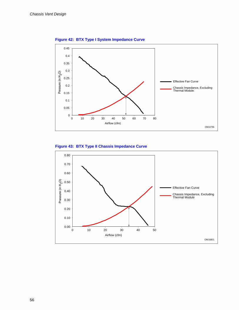
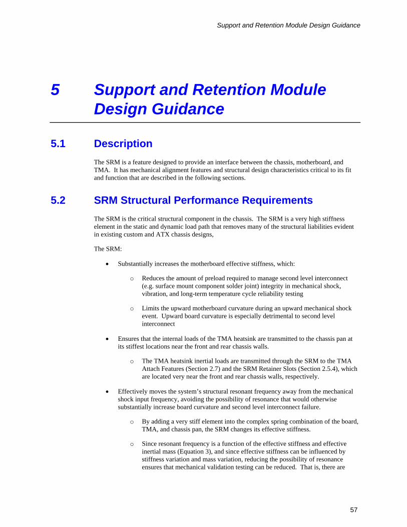
The loss coefficient in Table 3 can be used to generate the MASI impedance curves by using Equation 1or Equation 2. The MASI_I and MASI_II curves that result from the use of these equations and loss coefficients are illustrated in Figure 42 and Figure 43, respectively.
Equation 1: Maximum Acceptable System Impedance Curve Calculation in Mixed Units
∆P = ½*(ρ)*( L_MASI)*(Q)2 /1.12x109
where, ∆P = in H2O ρ = kg/m3 L_MASI = 1/m4 Q = Cubic Feet Per Minute
Equation 2: Maximum Acceptable System Impedance Curve Calculation in SI Units
∆P = ½*(ρ)*( L_MASI)*(Q)2/3600
where, ∆P = Pa ρ = kg/m3 L_MASI = 1/m4 Q = m3/min
Chassis Vent Design
56
Figure 42: BTX Type I System Impedance Curve
OM16796
0.4
0
0.35
0.3
0.25
0.2
0.15
0.1
0.05
0 10 20 30 40 50 60 70
Airflow (cfm)
80
0.45
Effective Fan Curve
Chassis Impedance, ExcludingThermal Module
Figure 43: BTX Type II Chassis Impedance Curve
OM16801
0.80
0.00
0.70
0.60
0.50
0.40
0.30
0.20
0.10
0 10 20 30 40
Airflow (cfm)
50
Effective Fan Curve
Chassis Impedance, ExcludingThermal Module
Support and Retention Module Design Guidance
57
5 Support and Retention Module Design Guidance
5.1 Description The SRM is a feature designed to provide an interface between the chassis, motherboard, and TMA. It has mechanical alignment features and structural design characteristics critical to its fit and function that are described in the following sections.
5.2 SRM Structural Performance Requirements The SRM is the critical structural component in the chassis. The SRM is a very high stiffness element in the static and dynamic load path that removes many of the structural liabilities evident in existing custom and ATX chassis designs,
The SRM:
• Substantially increases the motherboard effective stiffness, which:
o Reduces the amount of preload required to manage second level interconnect (e.g. surface mount component solder joint) integrity in mechanical shock, vibration, and long-term temperature cycle reliability testing
o Limits the upward motherboard curvature during an upward mechanical shock event. Upward board curvature is especially detrimental to second level interconnect
• Ensures that the internal loads of the TMA heatsink are transmitted to the chassis pan at its stiffest locations near the front and rear chassis walls.
o The TMA heatsink inertial loads are transmitted through the SRM to the TMA Attach Features (Section 2.7) and the SRM Retainer Slots (Section 2.5.4), which are located very near the front and rear chassis walls, respectively.
• Effectively moves the system’s structural resonant frequency away from the mechanical shock input frequency, avoiding the possibility of resonance that would otherwise substantially increase board curvature and second level interconnect failure.
o By adding a very stiff element into the complex spring combination of the board, TMA, and chassis pan, the SRM changes its effective stiffness.
o Since resonant frequency is a function of the effective stiffness and effective inertial mass (Equation 3), and since effective stiffness can be influenced by stiffness variation and mass variation, reducing the possibility of resonance ensures that mechanical validation testing can be reduced. That is, there are
Support and Retention Module Design Guidance
58
fewer combinations of mass and stiffness that need to be tested to ensure that the chassis design works in all probable conditions.
Equation 3: Resonant Frequency
ω α √(k eff /m eff)
Where
ω is the structural resonant frequency (Hz).
k eff is the effectiveness stiffness of the structure responding to the load generated by the accelerated effective mass (lb /in)
m eff is the effective mass accelerated by the mechanical shock event (lb).
o Note the many sources of possible variation listed below and the inclusion of the SRM in every chassis design can be easily justified as a necessary investment:
Board stiffness variation from board design, board suppliers, board manufacturing variation
Chassis stiffness from pan thickness variation, modulus variation
TMA stiffness variation from duct design, heatsink design, and duct manufacturing
TMA mass variation due to alternative TMA heatsink designs (for instance, one chassis often supports Value, Mainstream, and Performance processors, each with substantially different design characteristics)
Motherboard inertial mass variation due to component placement around the processor (e.g. voltage regulation components, memory controller heatsink)
As noted above, the SRM plays a substantial role in protecting motherboard second level interconnect (e.g. surface mount component solder joints) during the board movement caused by mechanical shock and /or vibration events. Intel elected to require the integration of the SRM in BTX-compliant chassis designs specifically for this purpose.
There is an industry initiative to migrate Desktop PC designs to lead-free components. Since leaded solder joints are considerably stronger than lead-free solder joints, system integrators are rightfully concerned about the structural design attributes of chassis and will select chassis designs based on their structural performance. Failing to do so will significantly increase the risk of mechanical validation and long-term reliability failures due to second level interconnect failures.
The BTX System Design Guide, available publicly at www.formfactors.org, is a document widely read by all system integrators in the Desktop PC industry, and it describes the validation liability associated with the migration to lead-free motherboards. These knowledgeable system integrators will request BTX chassis designs with the SRM.
SRM structural design recommendation:
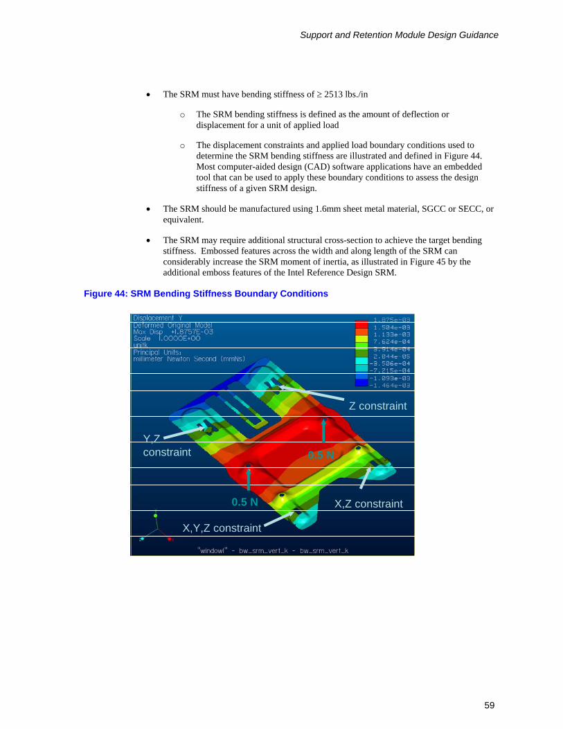
Support and Retention Module Design Guidance
59
• The SRM must have bending stiffness of ≥ 2513 lbs./in
o The SRM bending stiffness is defined as the amount of deflection or displacement for a unit of applied load
o The displacement constraints and applied load boundary conditions used to determine the SRM bending stiffness are illustrated and defined in Figure 44. Most computer-aided design (CAD) software applications have an embedded tool that can be used to apply these boundary conditions to assess the design stiffness of a given SRM design.
• The SRM should be manufactured using 1.6mm sheet metal material, SGCC or SECC, or equivalent.
• The SRM may require additional structural cross-section to achieve the target bending stiffness. Embossed features across the width and along length of the SRM can considerably increase the SRM moment of inertia, as illustrated in Figure 45 by the additional emboss features of the Intel Reference Design SRM.
Figure 44: SRM Bending Stiffness Boundary Conditions
0.5 N
0.5 NY,Z constraint
X,Y,Z constraint
X,Z constraint
Z constraint
0.5 N
0.5 NY,Z constraint
X,Y,Z constraint
X,Z constraint
Z constraint
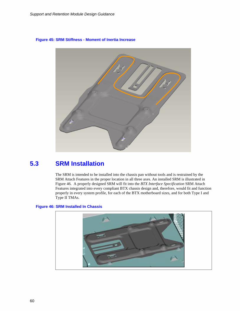
Support and Retention Module Design Guidance
60
Figure 45: SRM Stiffness - Moment of Inertia Increase
5.3 SRM Installation The SRM is intended to be installed into the chassis pan without tools and is restrained by the SRM Attach Features in the proper location in all three axes. An installed SRM is illustrated in Figure 46. A properly designed SRM will fit into the BTX Interface Specification SRM Attach Features integrated into every compliant BTX chassis design and, therefore, would fit and function properly in every system profile, for each of the BTX motherboard sizes, and for both Type I and Type II TMAs.
Figure 46: SRM Installed In Chassis
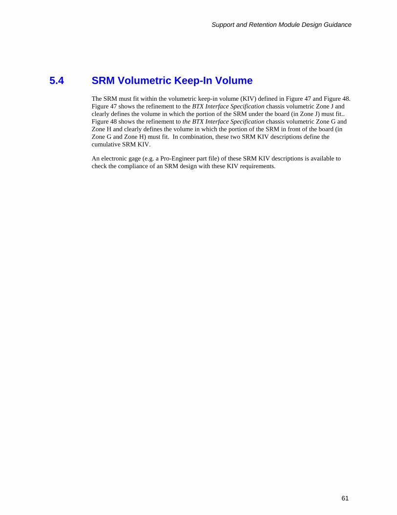
Support and Retention Module Design Guidance
61
5.4 SRM Volumetric Keep-In Volume The SRM must fit within the volumetric keep-in volume (KIV) defined in Figure 47 and Figure 48. Figure 47 shows the refinement to the BTX Interface Specification chassis volumetric Zone J and clearly defines the volume in which the portion of the SRM under the board (in Zone J) must fit.. Figure 48 shows the refinement to the BTX Interface Specification chassis volumetric Zone G and Zone H and clearly defines the volume in which the portion of the SRM in front of the board (in Zone G and Zone H) must fit. In combination, these two SRM KIV descriptions define the cumulative SRM KIV.
An electronic gage (e.g. a Pro-Engineer part file) of these SRM KIV descriptions is available to check the compliance of an SRM design with these KIV requirements.
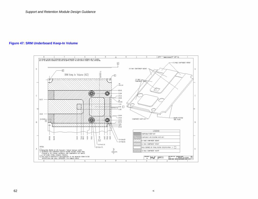
Support and Retention Module Design Guidance
62 <
Figure 47: SRM Underboard Keep-In Volume
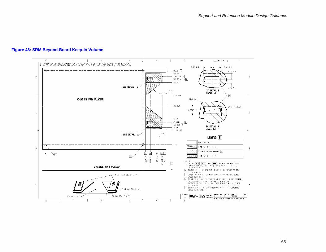
Support and Retention Module Design Guidance
63
Figure 48: SRM Beyond-Board Keep-In Volume
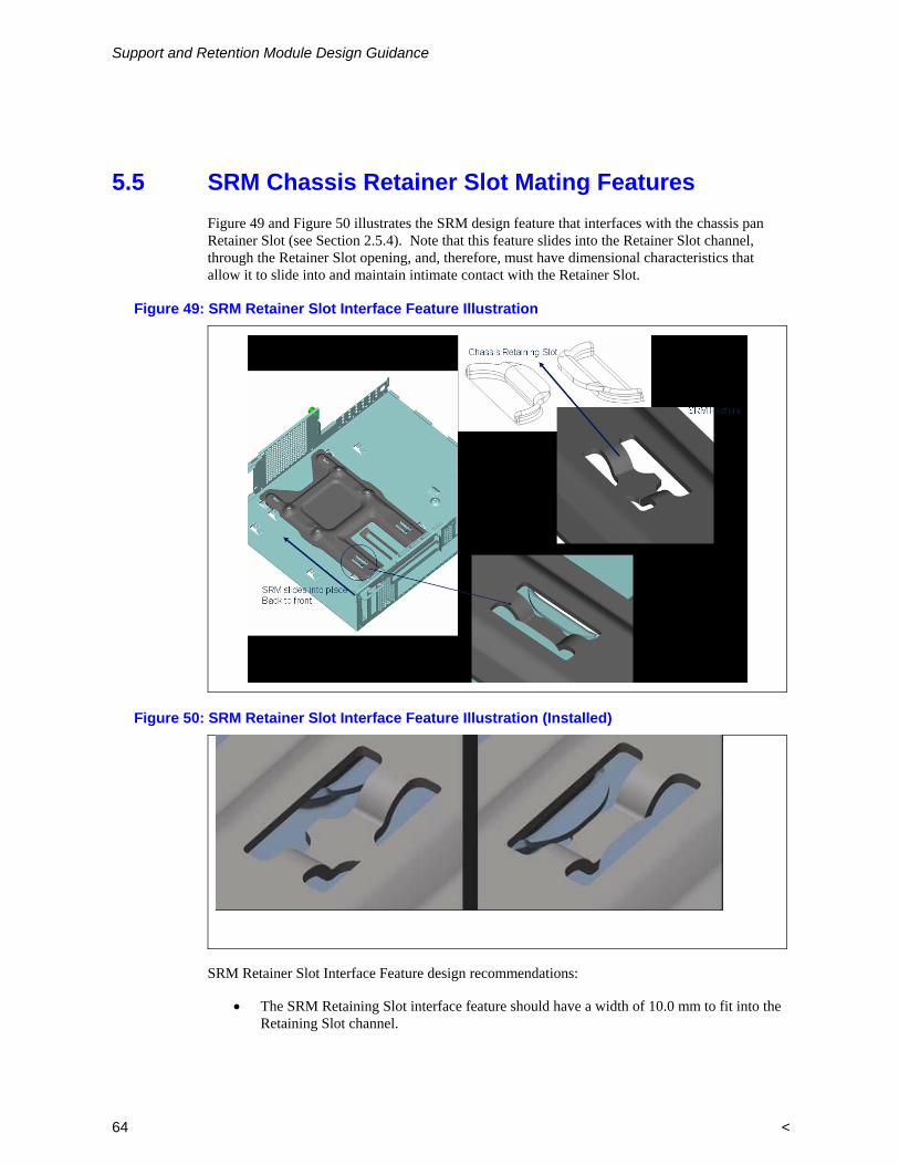
Support and Retention Module Design Guidance
64 <
5.5 SRM Chassis Retainer Slot Mating Features Figure 49 and Figure 50 illustrates the SRM design feature that interfaces with the chassis pan Retainer Slot (see Section 2.5.4). Note that this feature slides into the Retainer Slot channel, through the Retainer Slot opening, and, therefore, must have dimensional characteristics that allow it to slide into and maintain intimate contact with the Retainer Slot.
Figure 49: SRM Retainer Slot Interface Feature Illustration
Figure 50: SRM Retainer Slot Interface Feature Illustration (Installed)
SRM Retainer Slot Interface Feature design recommendations:
• The SRM Retaining Slot interface feature should have a width of 10.0 mm to fit into the Retaining Slot channel.

Support and Retention Module Design Guidance
• The SRM Retaining Slot interface feature should have a length of 3.0 mm to provide adequate contact against the channel contact surface.
• The SRM Retaining Slot interface feature should be connected to the SRM main body by extended arms of each end. These arms should have a maximum width of 5.0 mm to fit into and slide through the opening.
The SRM Retaining Slot interface feature is responsible for transferring TMA heatsink inertial loads to the chassis pan. In addition to using 1.6mm thickness sheet metal, Intel also recommends that the SRM designer use appropriate structural design practices in the selection of material grade, feature dimensions, and the SRM manufacturing process to ensure that the strength of this feature is sufficient.
5.6 SRM Chassis Front Guide Interface Features Figure 51 illustrates the SRM design feature that interfaces with the chassis pan Front Guide (see Section 2.5.1). Note that this SRM feature slides past the vertical guiding surface and under the horizontal guiding surface. The SRM is captured between the opposing vertical guiding surfaces of each Front Guide, and between the chassis pan and the horizontal guiding surfaces on each Front Guide. Therefore, the SRM must have dimensional characteristics that allow it to slide into and maintain intimate contact with both reference guiding surfaces of the Front Guide.
Figure 51: Front Guide Interface Feature Illustration
SRM Front Guide Interface design recommendations:
• In the area where the SRM will interface the Guiding Surface of the Front SRM Guides, the SRM width should be 145.0 ± 0.5 mm.
• In the area where the SRM will interface the horizontal guiding surface, the SRM thickness should be 2.1 ± 0.15 mm.
• The leading edge of the SRM, across the SRM width, should have lead-in to allow the SRM to be guided into position.
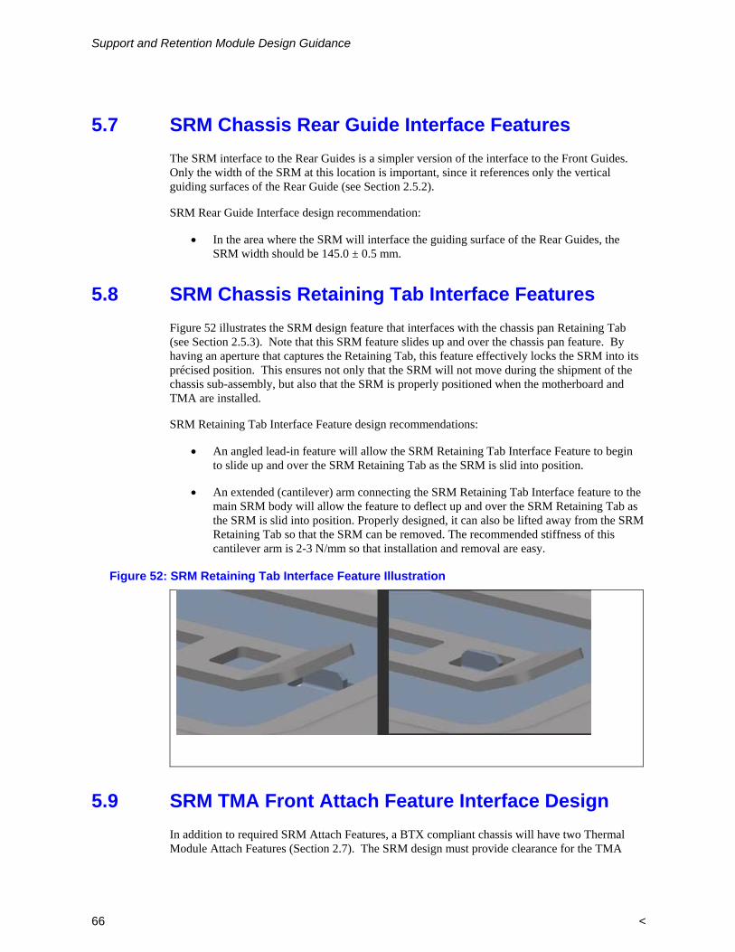
Support and Retention Module Design Guidance
66 <
5.7 SRM Chassis Rear Guide Interface Features The SRM interface to the Rear Guides is a simpler version of the interface to the Front Guides. Only the width of the SRM at this location is important, since it references only the vertical guiding surfaces of the Rear Guide (see Section 2.5.2).
SRM Rear Guide Interface design recommendation:
• In the area where the SRM will interface the guiding surface of the Rear Guides, the SRM width should be 145.0 ± 0.5 mm.
5.8 SRM Chassis Retaining Tab Interface Features Figure 52 illustrates the SRM design feature that interfaces with the chassis pan Retaining Tab (see Section 2.5.3). Note that this SRM feature slides up and over the chassis pan feature. By having an aperture that captures the Retaining Tab, this feature effectively locks the SRM into its précised position. This ensures not only that the SRM will not move during the shipment of the chassis sub-assembly, but also that the SRM is properly positioned when the motherboard and TMA are installed.
SRM Retaining Tab Interface Feature design recommendations:
• An angled lead-in feature will allow the SRM Retaining Tab Interface Feature to begin to slide up and over the SRM Retaining Tab as the SRM is slid into position.
• An extended (cantilever) arm connecting the SRM Retaining Tab Interface feature to the main SRM body will allow the feature to deflect up and over the SRM Retaining Tab as the SRM is slid into position. Properly designed, it can also be lifted away from the SRM Retaining Tab so that the SRM can be removed. The recommended stiffness of this cantilever arm is 2-3 N/mm so that installation and removal are easy.
Figure 52: SRM Retaining Tab Interface Feature Illustration
5.9 SRM TMA Front Attach Feature Interface Design In addition to required SRM Attach Features, a BTX compliant chassis will have two Thermal Module Attach Features (Section 2.7). The SRM design must provide clearance for the TMA
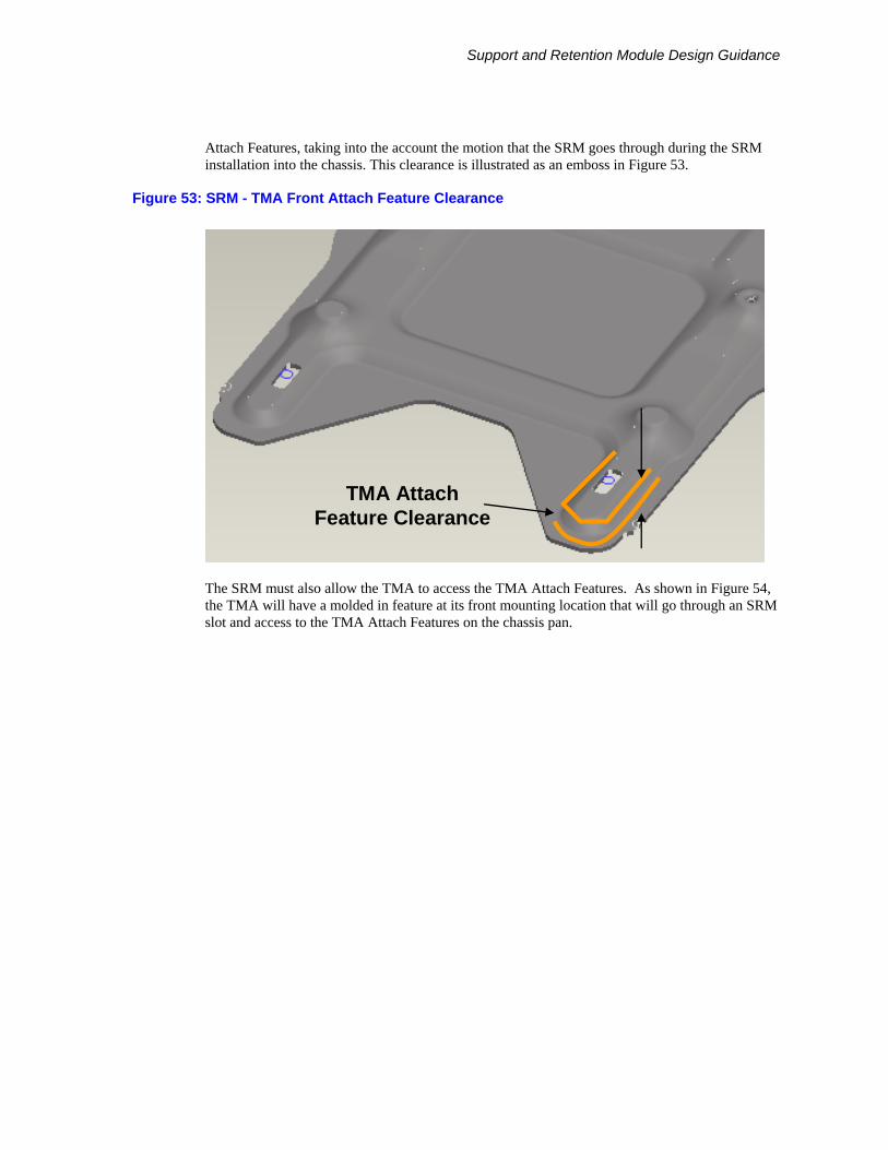
Support and Retention Module Design Guidance
Attach Features, taking into the account the motion that the SRM goes through during the SRM installation into the chassis. This clearance is illustrated as an emboss in Figure 53.
Figure 53: SRM - TMA Front Attach Feature Clearance
TMA AttachFeature Clearance
TMA AttachFeature Clearance
The SRM must also allow the TMA to access the TMA Attach Features. As shown in Figure 54, the TMA will have a molded in feature at its front mounting location that will go through an SRM slot and access to the TMA Attach Features on the chassis pan.
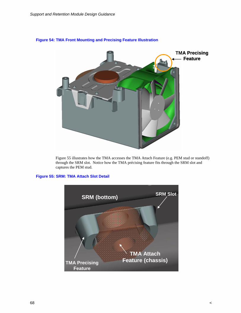
Support and Retention Module Design Guidance
68 <
Figure 54: TMA Front Mounting and Precising Feature Illustration
TMA PrecisingFeature
TMA PrecisingFeature
Figure 55 illustrates how the TMA accesses the TMA Attach Feature (e.g. PEM stud or standoff) through the SRM slot. Notice how the TMA précising feature fits through the SRM slot and captures the PEM stud.
Figure 55: SRM: TMA Attach Slot Detail
SRM (bottom)
TMA AttachFeature (chassis)
SRM Slot
TMA PrecisingFeature
SRM (bottom)
TMA AttachFeature (chassis)
SRM Slot
TMA PrecisingFeature
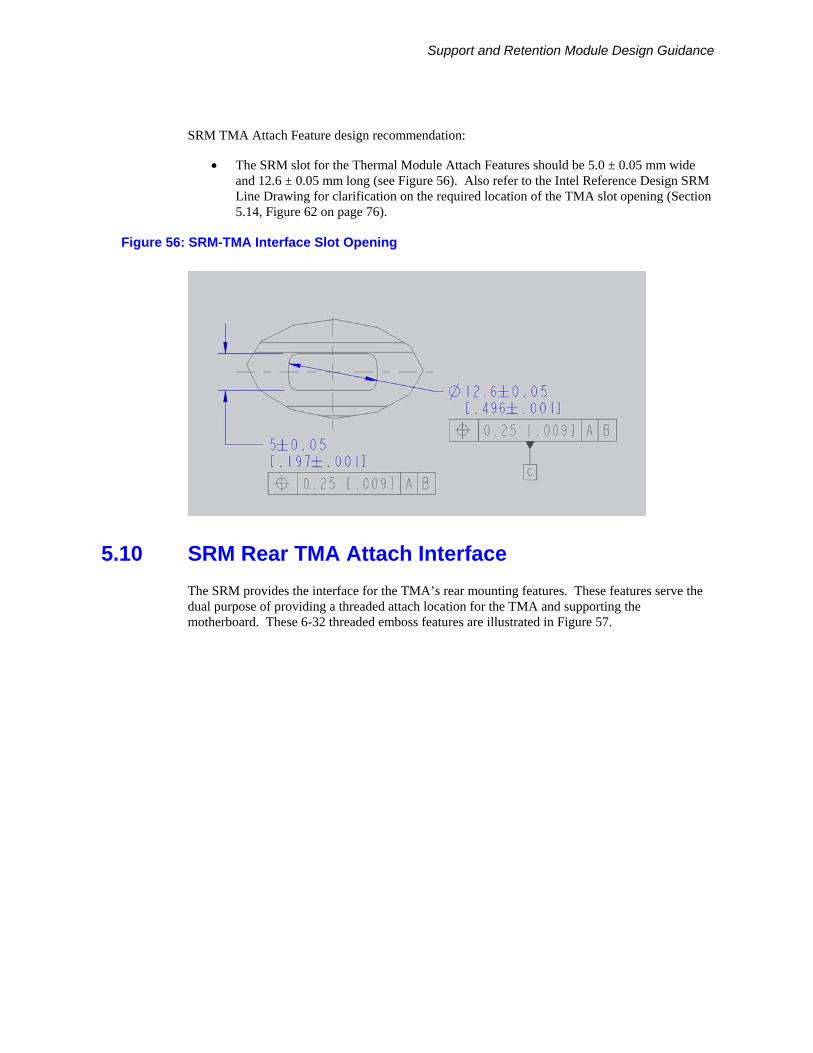
Support and Retention Module Design Guidance
SRM TMA Attach Feature design recommendation:
• The SRM slot for the Thermal Module Attach Features should be 5.0 ± 0.05 mm wide and 12.6 ± 0.05 mm long (see Figure 56). Also refer to the Intel Reference Design SRM Line Drawing for clarification on the required location of the TMA slot opening (Section 5.14, Figure 62 on page 76).
Figure 56: SRM-TMA Interface Slot Opening
5.10 SRM Rear TMA Attach Interface The SRM provides the interface for the TMA’s rear mounting features. These features serve the dual purpose of providing a threaded attach location for the TMA and supporting the motherboard. These 6-32 threaded emboss features are illustrated in Figure 57.
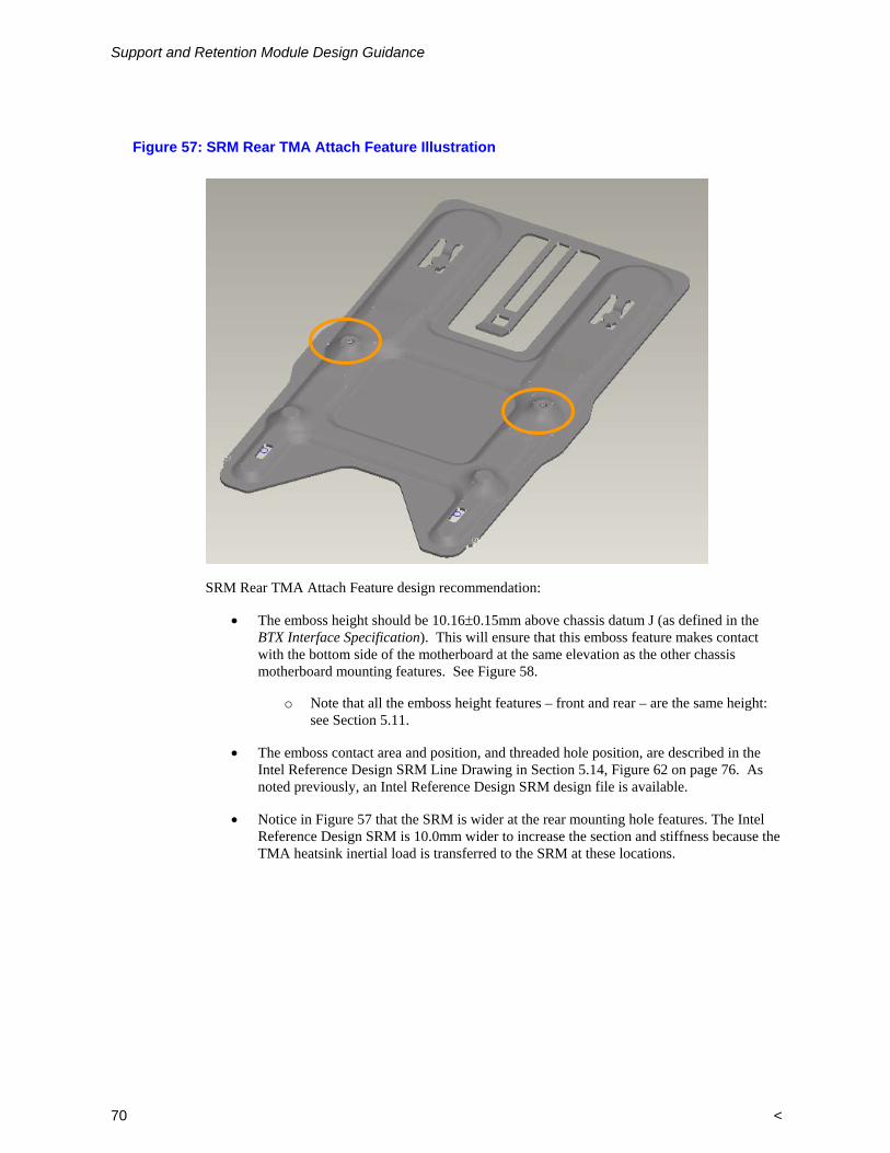
Support and Retention Module Design Guidance
70 <
Figure 57: SRM Rear TMA Attach Feature Illustration
SRM Rear TMA Attach Feature design recommendation:
• The emboss height should be 10.16±0.15mm above chassis datum J (as defined in the BTX Interface Specification). This will ensure that this emboss feature makes contact with the bottom side of the motherboard at the same elevation as the other chassis motherboard mounting features. See Figure 58.
o Note that all the emboss height features – front and rear – are the same height: see Section 5.11.
• The emboss contact area and position, and threaded hole position, are described in the Intel Reference Design SRM Line Drawing in Section 5.14, Figure 62 on page 76. As noted previously, an Intel Reference Design SRM design file is available.
• Notice in Figure 57 that the SRM is wider at the rear mounting hole features. The Intel Reference Design SRM is 10.0mm wider to increase the section and stiffness because the TMA heatsink inertial load is transferred to the SRM at these locations.
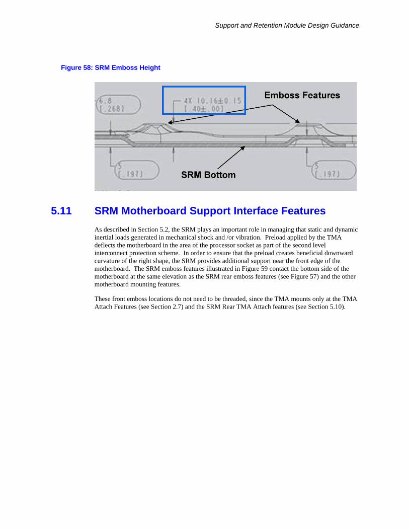
Support and Retention Module Design Guidance
Figure 58: SRM Emboss Height
5.11 SRM Motherboard Support Interface Features As described in Section 5.2, the SRM plays an important role in managing that static and dynamic inertial loads generated in mechanical shock and /or vibration. Preload applied by the TMA deflects the motherboard in the area of the processor socket as part of the second level interconnect protection scheme. In order to ensure that the preload creates beneficial downward curvature of the right shape, the SRM provides additional support near the front edge of the motherboard. The SRM emboss features illustrated in Figure 59 contact the bottom side of the motherboard at the same elevation as the SRM rear emboss features (see Figure 57) and the other motherboard mounting features.
These front emboss locations do not need to be threaded, since the TMA mounts only at the TMA Attach Features (see Section 2.7) and the SRM Rear TMA Attach features (see Section 5.10).
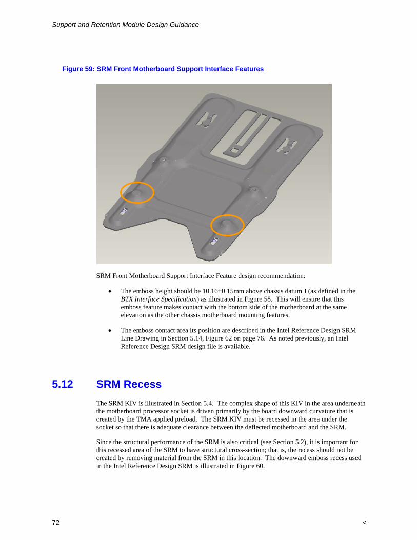
Support and Retention Module Design Guidance
72 <
Figure 59: SRM Front Motherboard Support Interface Features
SRM Front Motherboard Support Interface Feature design recommendation:
• The emboss height should be 10.16±0.15mm above chassis datum J (as defined in the BTX Interface Specification) as illustrated in Figure 58. This will ensure that this emboss feature makes contact with the bottom side of the motherboard at the same elevation as the other chassis motherboard mounting features.
• The emboss contact area its position are described in the Intel Reference Design SRM Line Drawing in Section 5.14, Figure 62 on page 76. As noted previously, an Intel Reference Design SRM design file is available.
5.12 SRM Recess The SRM KIV is illustrated in Section 5.4. The complex shape of this KIV in the area underneath the motherboard processor socket is driven primarily by the board downward curvature that is created by the TMA applied preload. The SRM KIV must be recessed in the area under the socket so that there is adequate clearance between the deflected motherboard and the SRM.
Since the structural performance of the SRM is also critical (see Section 5.2), it is important for this recessed area of the SRM to have structural cross-section; that is, the recess should not be created by removing material from the SRM in this location. The downward emboss recess used in the Intel Reference Design SRM is illustrated in Figure 60.
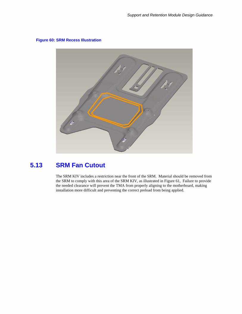
Support and Retention Module Design Guidance
Figure 60: SRM Recess Illustration
5.13 SRM Fan Cutout The SRM KIV includes a restriction near the front of the SRM. Material should be removed from the SRM to comply with this area of the SRM KIV, as illustrated in Figure 61, Failure to provide the needed clearance will prevent the TMA from properly aligning to the motherboard, making installation more difficult and preventing the correct preload from being applied.
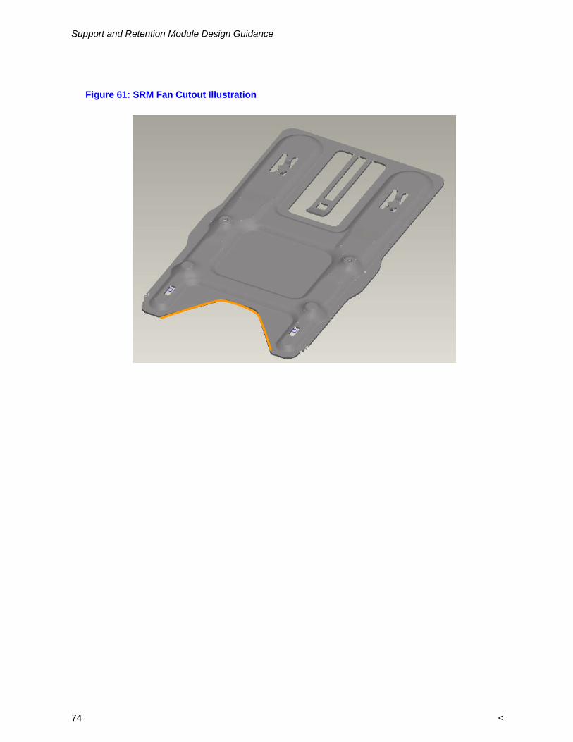
Support and Retention Module Design Guidance
74 <
Figure 61: SRM Fan Cutout Illustration
Support and Retention Module Design Guidance
5.14 SRM Reference Design Line Drawing
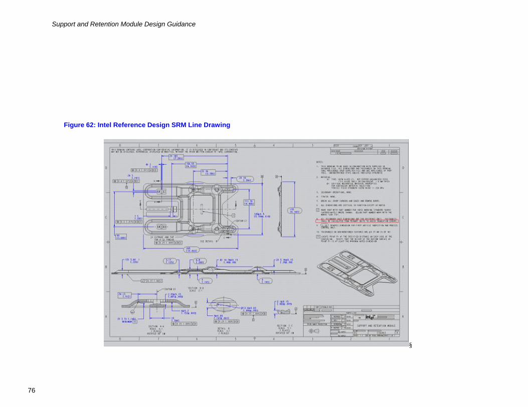
Support and Retention Module Design Guidance
76
Figure 62: Intel Reference Design SRM Line Drawing
§


![Sensors and Actuators B: Chemicalkllear/papers/EricksonSensActB14.pdfMar 25, 2014 · BTX contaminants at factors exceeding two orders of magnitude [23]. As BTX solutes (n≈1.5)](https://static.documents.pub/doc/80x56/5f927f0e5a1d18072513ae91/sensors-and-actuators-b-kllearpapersericksonsensactb14pdf-mar-25-2014-btx.jpg)


