BYOC Analog Delay Kit Instructions Please read through the instructions completely before beginning this project. This is one of our most difficult kits and it is a little different than other BYOC kits, so even if you are an experienced builder, take the time to look these instructions over in their entirety before beginning. Warranty: BYOC, LLC guarantees that your kit will be complete and that all parts and components will arrive as described, functioning and free of defect. Soldering, clipping, cutting, stripping, or using any of the components in any way voids this guarantee. BYOC, LLC guarantees that the instructions for your kit will be free of any majors errors that would cause you to permanently damage any components in your kit, but does not guarantee that the instructions will be free of typos or minor errors. BYOC, LLC does not warranty the completed pedal as a whole functioning unit nor do we warranty any of the individual parts once they have been used. If you have a component that is used, but feel it was defective prior to you using it, we reserve the right to determine whether or not the component was faulty upon arrival. Please direct all warranty issues to: [email protected]This would include any missing parts issues. Return: BYOC, LLC accepts returns and exchanges on all products for any reason, as long as they are unused. We do not accept partial kit returns. Returns and exchanges are for the full purchase price less the cost of shipping and/or any promotional pricing. Return shipping is the customers responsiblity. This responsibility not only includes the cost of shipping, but accountability of deliver as well. Please contact
Transcript
BYOC Analog Delay Kit Instructions
Please read through the instructions completely beforebeginning this project. This is one of our most difficult kits
and it is a little different than other BYOC kits, so even if youare an experienced builder, take the time to look these
instructions over in their entirety before beginning.
Warranty:BYOC, LLC guarantees that your kit will be complete and that all parts and componentswill arrive as described, functioning and free of defect. Soldering, clipping, cutting,stripping, or using any of the components in any way voids this guarantee. BYOC, LLCguarantees that the instructions for your kit will be free of any majors errors that wouldcause you to permanently damage any components in your kit, but does not guaranteethat the instructions will be free of typos or minor errors. BYOC, LLC does notwarranty the completed pedal as a whole functioning unit nor do we warranty any of theindividual parts once they have been used. If you have a component that is used, butfeel it was defective prior to you using it, we reserve the right to determine whether ornot the component was faulty upon arrival. Please direct all warranty issues to:[email protected] This would include any missing parts issues.
Return:BYOC, LLC accepts returns and exchanges on all products for any reason, as long asthey are unused. We do not accept partial kit returns. Returns and exchanges are for thefull purchase price less the cost of shipping and/or any promotional pricing. Returnshipping is the customers responsiblity. This responsibility not only includes the cost ofshipping, but accountability of deliver as well. Please contact
[email protected] to receieve a return authorization before mailing.
Tech Support:BYOC, LLC makes no promises or guarantees that you will sucessfully complete your kitin a satisfactory mannor. Nor does BYOC, LLC promise or guarantee that you willreceive any technical support. Purchasing a product from BYOC, LLC does not entitleyou to any amount of technical support. BYOC, LLC does not promise or guarantee thatany technical support you may receive will be able to resolve any or all issues you may beexperiencing.
That being said, we will do our best to help you as much as we can. Our philosophy atBYOC is that we will help you only as much as you are willing to help yourself. We havea wonderful and friendly DIY discussion forum with an entire section devoted to thetechnical support and modifications of BYOC kits.
www.buildyourownclone.com/board
When posting a tech support thread on the BYOC forum, please post it in the correctlounge, and please title your thread appropriately. If everyone titles their threadsHELP! , then it makes it impossible for the people who are helping you to keep track of
your progress. A very brief discription of your specific problem will do. It will also makeit easier to see if someone else is having or has had the same problem as you. Thequestion you are about to ask may already be answered. Here are a list of things that youshould include in the body of your tech support thread:1. A detailed explanation of what the problem is. (not just, It doesn t work, help )2. Pic of the top side of your PCB.3. Pic of the underside of your PCB.4. Pic that clearly shows your footswitch/jack wiring and the wires going to the PCB5. A pic that clearly shows your wiring going from the PCB to the pots and any otherswitches(only if your kit has non-PC mounted pots and switches)6. Is bypass working?7. Does the LED come on?8. If you answer yes to 6 and 7, what does the pedal do when it is "on"?9. Battery or adapter.(if battery, is it good? If adapter, what type?)
Also, please only post pics that are in focus. You're only wasting both parties' time if youpost out of focus, low res pics from your cell phone.Revision Notes:Rev 1.1 (current)Rev 1.0 - 4 x 10k resistors need to be replaced with 1k. 1 x 100k resistor needs to bereplaced with a 10k. 1 x 22k resistor needs to be replaced with a 15k. A trace needs tobe cut and jumpered with a 33k resistor. See pages 6 and 7 for more info.
Copyrights:All material in this document is copyright 2008 by BYOC, LLC
Hardware:1 - drilled enclosure w/ 4 screws1 - byoc analog delay kit circuit board1 - DPDT PC mounted toggle switch1 - 3PDT footswitch3 - knobs1 - AC adaptor jack3 - ¼ mono jack1 - red LEDhook-up wire
Populating the Circuit Board
Before you begin: This is only necessary for the Rev1.0 PCB. If you have a Rev1.1 orhigher, you do can ignore pages 6 & 7. Be aware there are several components that needto be changed. The four 10k (103) resistors highlighted in yellow should be changed to
1k. The 100k(104) resistor highlighted in green should be changed to 10k. The 22k(223)resistor highlighted in pink should be changed to 15k And the three 2N5088 transistorshighlighted in red should be changed to MPS6521 transistors. You will be reminded of
these changes when you get to the point where we add the transistors and again when weget to the resistors.
You'll also need to make a minor adjustment to the PCB. You will need to use a utilityknife, razor blade, exacto knife or something sharp to cut one of the traces on the bottom
side of the PCB . You will make the cut at the yellow line highlighted in the diagramabove. You will then need to add a 33k resistor to the bottom side of the PCB,
connecting it to the solder pads highlighted in red. You should save this for the step tillthe end of the populating the PCB process. You will be reminded.
STEP 1: Add the diodes. There are six 1N914 and 1 1N4001 diodes. Be sure tomatched the end of the diode with the stripe to the layout on the PCB. The stripped end
should go in the square solder pad.
STEP 2: Add the IC Sockets. DO NOT SOLDER THE ACTUAL CHIPS!!!! You willput the chips into the sockets in the Installing the ICs portion of the instructions. Seepage 22 - 23 for more details. Each socket has a notch in one end. You should match
that notch up with the layout on the PCB and solder the socket directly to the PCB.
STEP 3: Add the film capacitors. These are not polarized so they can be inserted into thePCB in either direction.
STEP 4: Add the transistors. Match the flat side of the transistor to the flat side of thelayout on the PCB. One MPSA18 goes in the space highlighted in yellow. One BS170
goes in the space highlighted in pink. One 2N5088 goes in the space highlighted inorange. And remember that three MPS6521 transistors go in the spaces highlighted in red
even though the PCB calls for 2N5088. If you have a Rev1.1 PCB or higher, the partsnumbers of the transistors will be labelled correctly.
STEP 5: Add the internal trimpots. Many people get confused by these because thetrimpot itself only has 3 legs, but the PCB has 5 holes. The PCB has 5 holes so that it canaccomodate a variety of different trimpot brands and models. There should only be one
way the trimpot will fit into the PCB without having to bend the legs.
STEP 6: Add the resistors. Resistors are not polarized, so it does not matter which endgoes in which solder pad. The resistors need to stand on end. Also, if you have two or
more resistors next to each other, you will need to alternate them so that the body of onetransistor is across from the next because there will not be enough room to stick two
resistor bodies next to each other.
Add the resistors. Remember that the four 10k resistors highlighted in yellow shouldactually be 1k, the 100k highlighted in green should actually be 10k, and the 22k
highlighted in pink should atually be 15k. If you have a Rev1.1 PCB or higher, theresistor spaces will be labelled correctly. A space for the 33k resistor has been added to
the PCB and should be soldered at this time.
STEP 7: Add the ceramic disc capacitors. These are not polarized and can be insertedinto the PCB in either direction.
STEP 8: Add the aluminum electrolytic capacitors. These are polarized. The positiveend will have a longer lead and should go in the square solder pad. The negative end will
have a shorter lead with a black strip running down the body of the capacitor.
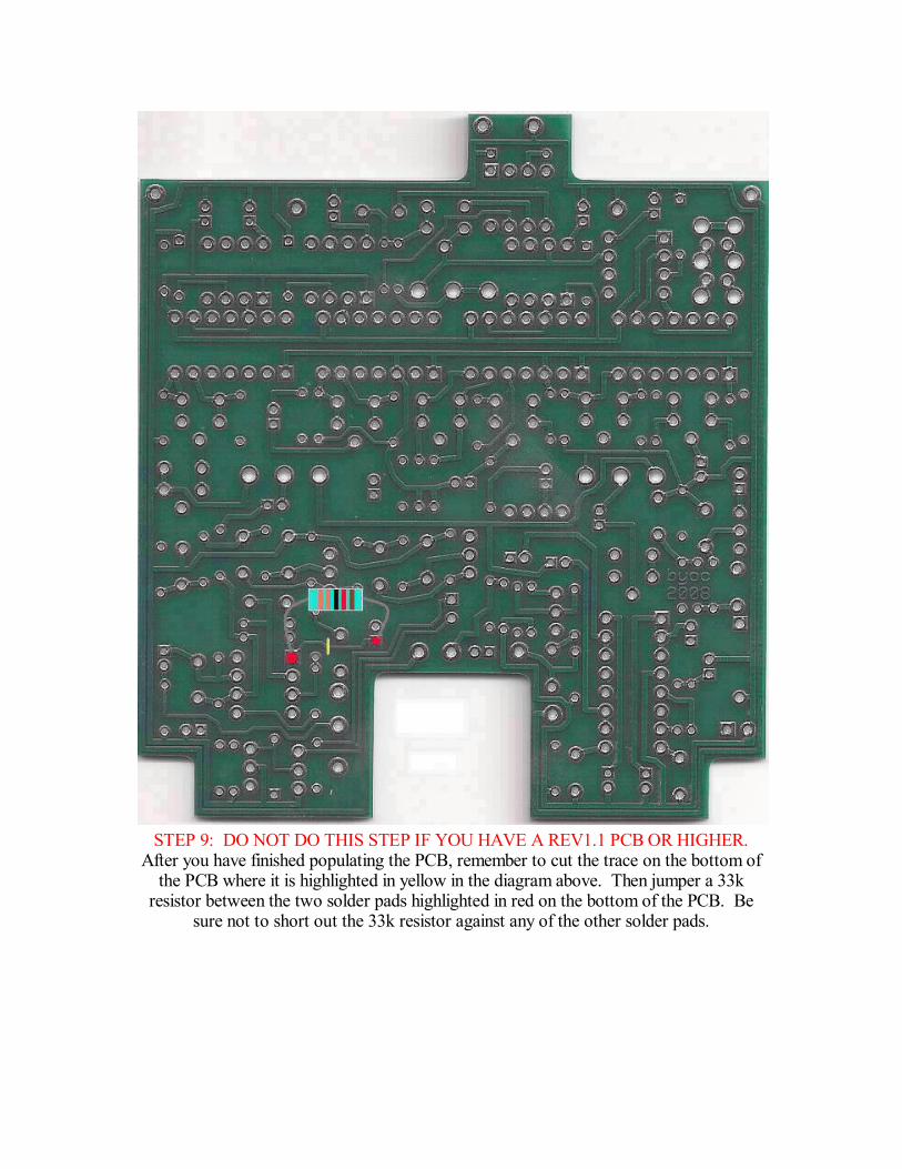
STEP 9: DO NOT DO THIS STEP IF YOU HAVE A REV1.1 PCB OR HIGHER.After you have finished populating the PCB, remember to cut the trace on the bottom of
the PCB where it is highlighted in yellow in the diagram above. Then jumper a 33kresistor between the two solder pads highlighted in red on the bottom of the PCB. Be
sure not to short out the 33k resistor against any of the other solder pads.
AssemblyStep 1: Mount the DC adaptor jack to the enclosure.
Step 2: Connect the TIP (negative) terminal of the DC adaptor jack to the - eyelet onthe PCB with 2 inches of hook up wire. Connect the SLEEVE of the DC adaptor jack tothe + eyelet on the PCB with 2 inches of hook up wire.
Step 3: Flip the PCB over so that the bottom or solder side is up. Insert the threepotentiometers, the LED, and the toggle switch into the bottom side of the PCB. DONOT SOLDER!!!There are only two ways in which the toggle switch can fit into the
PCB. Either way is fine. The LED will have one longer lead. The longer lead goes in thesquare solder pad. There will be two B100k potentiometers and one B1M potentiometer.The B1M pot is your delay time pot and should be mounted towards the top of the PCB.
The other two pots are for delay level and repeats.
Step 4: Hold the PCB in one hand so that the component side of the PCB is in the palm ofyour hand and the bottom side with the pots, toggle switch and LED is facing up. Nowuse your other hand to guide the predrilled enclosure onto the PCB assembly so that thepots, toggle switch and LED all go into there respective holes. Once the PCB assembly isin place, secure it by screwing on the washers and nuts for the pots and toggle switch.Only tighten them with your fingers. You do not want them very tight yet. Be sure tokeep your hand on the PCB so that it does not fall off the PC mounting posts of the potsand toggle switch.
Step 5: Turn the entire pedal over so that the component side of the PCB if facing up.Lift the PCB up off the pots and toggle switch about 2mm just to make sure that the backof the PCB does not short out against that pots. Make sure the PCB is level andsymetrically seated inside the enclosure.
Step 6: Solder the pots, PCB, and LED. You will solder these parts on the componentside of the PCB. After you have soldered them in place, be sure to tighten up their nuts.
Wiring the jacks, footswitch, andtoggle switch
Step 1: Install the 1/4 jacks to the enclosure. Be sure to turn the OUT jacks 1/4 turncounter clockwise so that their prongs do not short out against the delay time pot.
Step 2: Install the footswitch to the enclosure. It will have a white nylon washer and asilver metal washer. You can decide which washer you want to be visible on the outsideof the enclosure.
Step 3. Wire and solder the footswitch and 1/4 jacks according to the wiring diagram onthe next page.
Step 4: Wire the ABCD jumpers. Use 4 pieces of wire approx. 3 long. You aresimply connecting the A eyelet next to the toggle switch with the A eyelet moretowards the center of the PCB. And B to B , C to C , and D to D . Wire the Cand D eyelets first. Then wire the A and B eyelets.
Installing the ICs
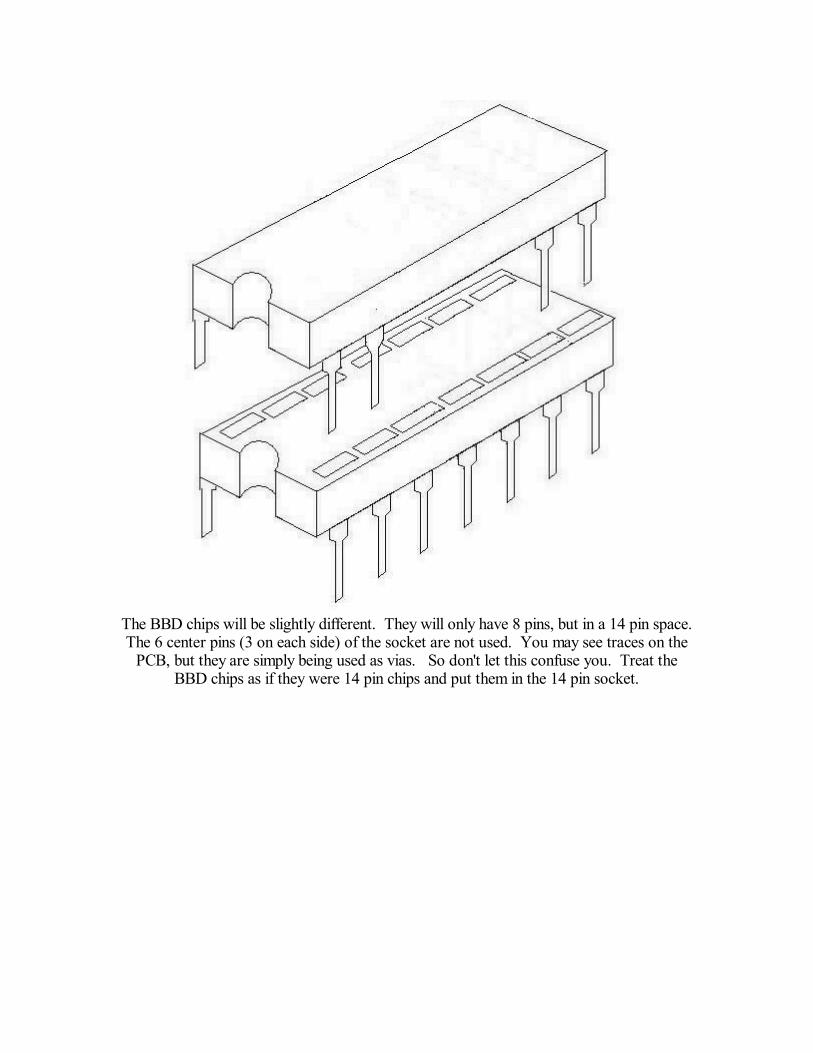
The BBD chips will be slightly different. They will only have 8 pins, but in a 14 pin space.The 6 center pins (3 on each side) of the socket are not used. You may see traces on the
PCB, but they are simply being used as vias. So don't let this confuse you. Treat theBBD chips as if they were 14 pin chips and put them in the 14 pin socket.
Setting up the Internal TrimpotsStep 1: Set all of the trimpots to noon.
Step 2: Set the delay level and repeats knobs to full turn clockwise. Set the delay timeknob for noon.
Step 3: Set the long/short switch for short delay time. The toggle bat would be pointingdown towards the footswitch in short mode.
Step 4: At this point, your delay should not be producing any echoes, so do not worryabout that. Adjust the BIAS1 trimmer untill you hear the repeats start to echo. Find theworking range of the BIAS1 trimmer. Set the trimmer so that it is in the middle of this
range. Now tweek the trimmer very carefully in either direction so that it gives you thebest sounding repeats. Use your ears for this step.
Step 5: Set the F.B. trimmer. F.B. stands for FeedBack threshold. You want to set thistrimmer to taste. Turning it clockwise will inscrease the sensitivity of the repeats knob.Keep in mind that your repeats knob is at full turn clockwise (or it should be....doublecheck) while setting the F.B. trimmer. So you want to set this trimmer so that yourechoes behave the way you want them to when your repeats knob is full turn clockwise.If you only want infinite repeats, but don't want self-oscillation (run-aways repeats), thenadjust the F.B. trimmer accordingly. And if you want self-oscillation, then adjust the F.B.trimmer accordingly.
Step 6: Set the BIAS2 trimmer. The first thing you must do is MAKE SURE THELONG/SHORT SWITCH IS IN LONG MODE! Flip the toggle bat so that it ispointing up towards the jacks. You should not hear any echoes again. Now adjusts theBIAS2 trimmer so that you can hear echoes. Now find the working range of thetrimpot and set it in the middle. Now use your ears to find the best sounding repeats.
Step 7: Adjust the BAL trimmer. BAL is short for balance. It adjusts the output of thedelay line when all 4 BBD stages are engaged. You want to set the BAL trimmer so thatthe output of all 4 BBD stages in long mode are the same as the output of just the oneBBD stage in short mode. This is almost impossible to do. But if you think of the BALtrimmer as being the F.B. trimmer for long mode, then it is very easy to set up. Simpleturn your BAL knob so that the repeats knob behaves the same in long mode as it does inshort mode. If you do this, then it means that the output of all 4 BBD stages is the sameas the output of only the first BBD stage. Note - Turning the BAL trimmer counterclockwisw will increase output.
Step 8: Adjust all the CAN trimmers. YOU WILL NEED TO USE THE SIGNALTESTER FOR THIS. CAN is short for cancel. The goal here is to adjust each trimmer tocancel out as much clock noise as possible. CAN1 is the cancel trimmer for BBD1.CAN2 is the cancel trimmer for BBD2. And so on... The red dot is the check pointwhere you will place the Signal Tester when adjusting the CAN1 trimmer which is alsohighlighted in red. The pink dot is the check point where you will place the Signal Testerwhen adjusting the CAN2 trimmer which is also highlighted in pink. And so on... Notethat the first 3 check points are Pins 7 of the 2nd, 3rd, and 4th BBD chips. This is becausePin 7 is the input of each BBD. So this also makes Pin 7 the ultimate output of theprevious BBD. This is why we test the output of the first BBD at the input of theSeccond BBD. And the output of the second BBD at the input of the third BBD. And soon.... Until we get to the last BBD. When adjusting the CAN4 trimmer, the check pointwill be lug 3 of the BAL trimmer highlighted in green. Lug 3 of the BAL trimmer shouldhave some exposed metal on the top of the trimpot iself which should make this fairlyeasy. Ok....so here we go... This is going to be loud and noisy and will give you a new
appreciation for how much noise the compander chip removes. You will hear a loud hissing noise with avery high pitched squeel on top of it. Start with the CAN1 trimmer and check point. Experiment byturning the trimmer full turn in both directions so you can hear what it does. You should notice that thefarther you get from center, the louder the high pitched noise will become. This is the clock noise that weare trying to dial out. So somewhere around noon on the trimpot, but usually not exactly, is where youwant to set it. Repeat this process for all 4 of the CAN trimmers.
Step 9: Adjust the clock trimmer. The clock trimmer will set the maximum amount of delay time anddial out the clocknoise. It's a give and take. The more delay time you have, the noisier it will be. Usuallynoon, or just shy of noon will give you about 1 second of delay time when the delay time knob is maxed.800ms should be about 4 or 5 o'clock on the trimmer and should be where you get almost no clock noise atall. A note about noise - If you've never played an analog delay, you should know that there will alwaysbe some element of noise. Each repeat should sound like it's riding on top of a little cloud of noise. Itshouldn't be excessive or too terribly annoying (if it is, then maybe you need to stick to digital delay) butjust be aware, there will always be some element of graininess and noise with associated with analogdelay.