The C8051F12x Development Kit contains the following items:
• C8051F120 Target Board• C8051Fxxx Development Kit Quick-Start Guide• Silicon Laboratories IDE and Product Information CD-ROM. CD content includes:
• Silicon Laboratories Integrated Development Environment (IDE)• Keil 8051 Development Tools (macro assembler, linker, evaluation ‘C’ compiler)• Source code examples and register definition files• Documentation• C8051F12x Development Kit User’s Guide (this document)
• AC to DC Power Adapter• USB Debug Adapter (USB to Debug Interface)• USB Cable
2. Hardware Setup using a USB Debug Adapter
The target board is connected to a PC running the Silicon Laboratories IDE via the USB Debug Adapter as shownin Figure 1.
1. Connect the USB Debug Adapter to the JTAG connector on the target board with the 10-pin ribbon cable.2. Connect one end of the USB cable to the USB connector on the USB Debug Adapter. 3. Connect the other end of the USB cable to a USB Port on the PC.4. Connect the ac/dc power adapter to power jack P1 on the target board.
Notes:• Use the Reset button in the IDE to reset the target when connected using a USB Debug Adapter.• Remove power from the target board and the USB Debug Adapter before connecting or disconnecting the
ribbon cable from the target board. Connecting or disconnecting the cable when the devices have power can damage the device and/or the USB Debug Adapter.
Figure 1. Hardware Setup using a USB Debug Adapter
PC
USB Cable
USB Debug Adapter
AC/DCAdapter
Target Board
SILICON LABORATORIES
PWR
P1.6
P3
.7R
ES
ET
Port 4Port 3Port 1
Port 2 Port 0
MCU
Silico
n Lab
oratories
US
B D
EB
UG
AD
AP
TE
R
Ru
n
Stop
Pow
er
C8051F12x-DK
2 Rev. 0.7
3. Software Setup
The included CD-ROM contains the Silicon Laboratories Integrated Development Environment (IDE), Keil software8051 tools and additional documentation. Insert the CD-ROM into your PC’s CD-ROM drive. An installer will auto-matically launch, allowing you to install the IDE software or read documentation by clicking buttons on the Installa-tion Panel. If the installer does not automatically start when you insert the CD-ROM, run autorun.exe found in theroot directory of the CD-ROM. Refer to the readme.txt file on the CD-ROM for the latest information regardingknown IDE problems and restrictions.
4. Silicon Laboratories Integrated Development Environment
The Silicon Laboratories IDE integrates a source-code editor, source-level debugger and in-system Flash program-mer. The use of third-party compilers and assemblers is also supported. This development kit includes the KeilSoftware A51 macro assembler, BL51 linker and evaluation version C51 ‘C’ compiler. These tools can be usedfrom within the Silicon Laboratories IDE.
4.1. System RequirementsThe Silicon Laboratories IDE requirements:
• Pentium-class host PC running Microsoft Windows 98SE or later.• One available COM or USB port.• 64 MB RAM and 40 MB free HD space recommended.
4.2. Assembler and LinkerA full-version Keil A51 macro assembler and BL51 banking linker are included with the development kit and areinstalled during IDE installation. The complete assembler and linker reference manual can be found under the Helpmenu in the IDE or in the “SiLabs\MCU\hlp” directory (A51.pdf).
4.3. Evaluation C51 ‘C’ CompilerAn evaluation version of the Keil C51 ‘C’ compiler is included with the development kit and is installed during IDEinstallation. The evaluation version of the C51 compiler is the same as the full professional version except codesize is limited to 4 kB and the floating point library is not included. The C51 compiler reference manual can befound under the Help menu in the IDE or in the “SiLabs\MCU\hlp” directory (C51.pdf).
4.4. Using the Keil Software 8051 Tools with the Silicon Laboratories IDETo perform source-level debugging with the IDE, you must configure the Keil 8051 tools to generate an absoluteobject file in the OMF-51 format with object extensions and debug records enabled. You may build the OMF-51absolute object file by calling the Keil 8051 tools at the command line (e.g. batch file or make file) or by using theproject manager built into the IDE. The default configuration when using the Silicon Laboratories IDE projectmanager enables object extension and debug record generation. Refer to Applications Note AN104 - IntegratingKeil 8051 Tools Into the Silicon Laboratories IDE in the “SiLabs\MCU\Documentation\Appnotes” directory on theCD-ROM for additional information on using the Keil 8051 tools with the Silicon Laboratories IDE.
To build an absolute object file using the Silicon Laboratories IDE project manager, you must first create a project. Aproject consists of a set of files, IDE configuration, debug views, and a target build configuration (list of files and toolconfigurations used as input to the assembler, compiler, and linker when building an output object file).
The following sections illustrate the steps necessary to manually create a project with one or more source files, builda program and download the program to the target in preparation for debugging. (The IDE will automatically create asingle-file project using the currently open and active source file if you select Build/Make Project before a project isdefined.)
C8051F12x-DK
Rev. 0.7 3
4.4.1. Creating a New Project
1. Select ProjectNew Project to open a new project and reset all configuration settings to default.
2. Select FileNew File to open an editor window. Create your source file(s) and save the file(s) with a rec-ognized extension, such as .c, .h, or .asm, to enable color syntax highlighting.
3. Right-click on “New Project” in the Project Window. Select Add files to project. Select files in the filebrowser and click Open. Continue adding files until all project files have been added.
4. For each of the files in the Project Window that you want assembled, compiled and linked into the targetbuild, right-click on the file name and select Add file to build. Each file will be assembled or compiled asappropriate (based on file extension) and linked into the build of the absolute object file.
Note: If a project contains a large number of files, the “Group” feature of the IDE can be used to organize. Right-click on “New Project” in the Project Window. Select Add Groups to project. Add pre-defined groups or add customized groups. Right-click on the group name and choose Add file to group. Select files to be added. Continue adding files until all project files have been added.
4.4.2. Building and Downloading the Program for Debugging
1. Once all source files have been added to the target build, build the project by clicking on the Build/MakeProject button in the toolbar or selecting ProjectBuild/Make Project from the menu.
Note: After the project has been built the first time, the Build/Make Project command will only build the files that have been changed since the previous build. To rebuild all files and project dependencies, click on the Rebuild All button in the toolbar or select ProjectRebuild All from the menu.
2. Before connecting to the target device, several connection options may need to be set. Open theConnection Options window by selecting OptionsConnection Options... in the IDE menu. First, selectthe appropriate adapter in the “Serial Adapter” section. Next, the correct “Debug Interface” must be selected.C8051F12x family devices use the JTAG debug interface. Once all the selections are made, click the OKbutton to close the window.
3. Click the Connect button in the toolbar or select DebugConnect from the menu to connect to the device.
4. Download the project to the target by clicking the Download Code button in the toolbar.
Note: To enable automatic downloading if the program build is successful select Enable automatic con-nect/download after build in the ProjectTarget Build Configuration dialog. If errors occur during the build process, the IDE will not attempt the download.
5. Save the project when finished with the debug session to preserve the current target build configuration,editor settings and the location of all open debug views. To save the project, select Project->Save ProjectAs... from the menu. Create a new name for the project and click on Save.
C8051F12x-DK
4 Rev. 0.7
5. Example Source Code
Example source code and register definition files are provided in the “SiLabs\MCU\Examples\C8051F12x” directoryduring IDE installation. These files may be used as a template for code development. Example applications includea blinking LED example which configures the green LED on the target board to blink at a fixed rate.
5.1. Register Definition FilesRegister definition files C8051F120.inc and C8051F120.h define all SFR registers and bit-addressable control/status bits. They are installed into the “SiLabs\MCU\Examples\C8051F12x” directory during IDE installation. Theregister and bit names are identical to those used in the C8051F12x data sheet. Both register definition files arealso installed in the default search path used by the Keil Software 8051 tools. Therefore, when using the Keil 8051tools included with the development kit (A51, C51), it is not necessary to copy a register definition file to eachproject’s file directory.
5.2. Code Banking FilesIn order to utilize code banking in a project there are two files that will need to be changed. You can either customedit L51_bank.a51 and startup.a51 or use the copies installed into the “IDEfiles\C51\Lib” directory during IDEinstallation. Both of these files MUST be added to your project and linked with your project in order for code bank-ing to function properly. For more information on code banking, please see Application Note AN130 - Code Bank-ing Using the Keil 8051 Tools.
5.3. Blinking LED ExampleThe example source files blink.asm and blinky.c show examples of several basic C8051F12x functions. Theseinclude; disabling the watchdog timer (WDT), configuring the Port I/O crossbar, configuring a timer for an interruptroutine, initializing the system clock, and configuring a GPIO port. When compiled/assembled and linked this pro-gram flashes the green LED on the C8051F120 target board about five times a second using the interrupt handlerwith a C8051F120 timer.
C8051F12x-DK
Rev. 0.7 5
6. Target Board
The C8051F12x Development Kit includes a target board with a C8051F120 device pre-installed for evaluation andpreliminary software development. Numerous input/output (I/O) connections are provided to facilitate prototypingusing the target board. Refer to Figure 2 for the locations of the various I/O connectors.
P1 Power connector (accepts input from 7 to 15 VDC unregulated power adapter)J1 Connects SW2 to P3.7 pinJ3 Connects LED D3 to P1.6 pinJ4 JTAG connector for Debug Adapter interface J5 DB-9 connector for UART0 RS232 interfaceJ6 Connector for UART0 TX (P0.0)J8 Connector for UART0 RTS (P4.0)J9 Connector for UART0 RX (P0.1)J10 Connector for UART0 CTS (P4.1)J11 Analog loopback connectorJ12–J19 Port 0–7 connectorsJ20 Analog I/O terminal blockJ22 VREF connectorJ23 VDD Monitor DisableJ24 96-pin Expansion I/O connector
Figure 2. C8051F120 Target Board
C8051F12X
J1
JTA
GR
ES
ET
P3
.7
P1
J24
Pin 1
Pin 1
Pin 1
J11
Pin 2
J3
J23
PWR
P1.6
J5
J20
Pin 1
Pin 2 J22
Pin 2
Pin 1
Port 0 Port 2
Port 4 Port 7 Port 1
Port 3Port 6Port 5
J4
J9J6J8J10
Pin 1
C8051F12x-DK
6 Rev. 0.7
6.1. System Clock SourcesThe C8051F120 device installed on the target board features a calibrated programmable internal oscillator which isenabled as the system clock source on reset. After reset, the internal oscillator operates at a frequency of3.0625MHz (+/-2%) by default but may be configured by software to operate at other frequencies. Therefore, inmany applications an external oscillator is not required. However, an external 22.1184 MHz crystal is installed on thetarget board for additional applications. Refer to the C8051F12x data sheet for more information on configuring thesystem clock source.
6.2. Switches and LEDsTwo switches are provided on the target board. Switch SW1 is connected to the RESET pin of the C8051F120.Pressing SW1 puts the device into its hardware-reset state. Switch SW2 is connected to the C8051F120’s generalpurpose I/O (GPIO) pin through headers. Pressing SW2 generates a logic low signal on the port pin. Remove theshorting block from the header to disconnect SW2 from the port pins. The port pin signal is also routed to a pin onthe J24 I/O connector. See Table 1 for the port pins and headers corresponding to each switch.
Two LEDs are also provided on the target board. The red LED labeled PWR is used to indicate a power connectionto the target board. The green LED labeled with a port pin name is connected to the C8051F120’s GPIO pinthrough headers. Remove the shorting block from the header to disconnect the LED from the port pin. The port pinsignal is also routed to a pin on the J24 I/O connector. See Table 1 for the port pins and headers corresponding toeach LED.
6.3. Target Board JTAG Interface (J4)The JTAG connector (J4) provides access to the JTAG pins of the C8051F120. It is used to connect the SerialAdapter or the USB Debug Adapter to the target board for in-circuit debugging and Flash programming. Table 2 shows the JTAG pin definitions.
Table 1. Target Board I/O Descriptions
Description I/O HeaderSW1 Reset none
SW2 P3.7 J1
Green LED P1.6 J3
Red LED PWR none
Table 2. JTAG Connector Pin Descriptions
Pin # Description1 +3VD (+3.3VDC)
2, 3, 9 GND (Ground)
4 TCK
5 TMS
6 TDO
7 TDI
8, 10 Not Connected
C8051F12x-DK
Rev. 0.7 7
6.4. Serial Interface (J5)A RS232 transceiver circuit and DB-9 (J5) connector are provided on the target board to facilitate serial connec-tions to UART0 of the C8051F120. The TX, RX, RTS and CTS signals of UART0 may be connected to the DB-9connector and transceiver by installing shorting blocks on headers J6, J8, J9 and J10.
J6 - Install shorting block to connect UART0 TX (P0.0) to the transceiver.J9 - Install shorting block to connect UART0 RX (P0.1) to the transceiver.J8 - Install shorting block to connect UART0 RTS (P4.0) to the transceiver.J10 - Install shorting block to connect UART0 CTS (P4.1) to the transceiver.
6.5. Analog I/O (J11, J20)Several C8051F120 analog signals are routed to the J20 terminal block and the J11 header. The J11 connectorprovides the ability to connect DAC0 and DAC1 outputs to several different analog inputs by installing a shortingblock between a DAC output and an analog input on adjacent pins of J11. Refer to Table 3 for J20 terminal blockconnections and Table 4 for J11 pin definitions.
Table 3. J20 Terminal Block Pin Descriptions
Pin # Description1 CP0+
2 CP0-
3 DAC0
4 DAC1
5 AIN0.0
6 AIN0.1
7 VREF0
8 ADND (Analog Ground)
Table 4. J11 Connector Pin Descriptions
Pin # Description1 CP0+
2 CP0-
3 DAC0
4 DAC1
5 CP1+
6 CP1-
7 AIN0.0
8 AIN0.1
9 DAC0
10 DAC1
11 AIN0.6
12 AIN0.7
C8051F12x-DK
8 Rev. 0.7
6.6. PORT I/O Connectors (J12 - J19)In addition to all port I/O signals being routed to the 96-pin expansion connector, each of the eight parallel ports ofthe C8051F120 has its own 10-pin header connector. Each connector provides a pin for the corresponding portpins 0-7, +3.3 VDC and digital ground. Table 5 defines the pins for the port connectors. The same pin-out order isused for all of the port connectors.
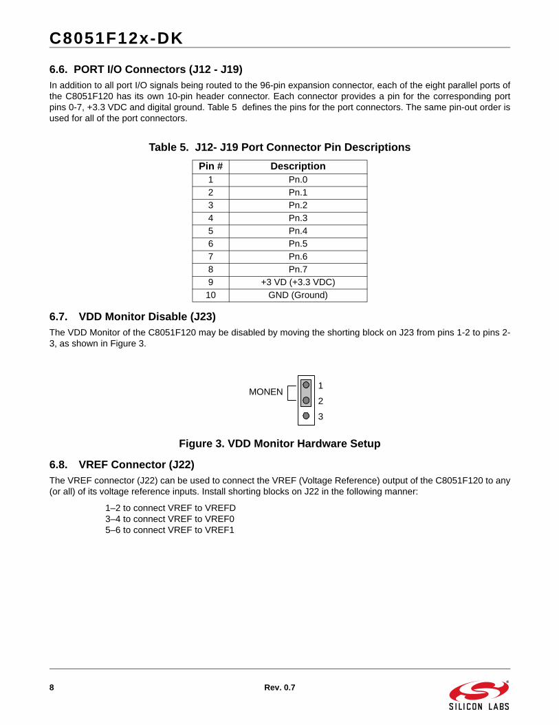
6.7. VDD Monitor Disable (J23)The VDD Monitor of the C8051F120 may be disabled by moving the shorting block on J23 from pins 1-2 to pins 2-3, as shown in Figure 3.
Figure 3. VDD Monitor Hardware Setup
6.8. VREF Connector (J22)The VREF connector (J22) can be used to connect the VREF (Voltage Reference) output of the C8051F120 to any(or all) of its voltage reference inputs. Install shorting blocks on J22 in the following manner:
1–2 to connect VREF to VREFD3–4 to connect VREF to VREF05–6 to connect VREF to VREF1
Table 5. J12- J19 Port Connector Pin Descriptions
Pin # Description1 Pn.0
2 Pn.1
3 Pn.2
4 Pn.3
5 Pn.4
6 Pn.5
7 Pn.6
8 Pn.7
9 +3 VD (+3.3 VDC)
10 GND (Ground)
1
3
2MONEN
C8051F12x-DK
Rev. 0.7 9
6.9. Expansion I/O Connector (J24)The 96-pin expansion I/O connector J24 is used to connect daughter boards to the main target board. J24 providesaccess to many C8051F120 signal pins. Pins for +3 V, digital ground, analog ground and the unregulated powersupply (VUNREG) are also available. The VUNREG pin is connected directly to the unregulated +V pin of the P1power connector. See Table 6 for a complete list of pins available at J24.
The J24 socket connector is manufactured by Hirose Electronic Co. Ltd, part number PCN13-96S-2.54DS, Digi-Key part number H7096-ND. The corresponding plug connector is also manufactured by Hirose Electronic Co. Ltd,part number PCN10-96P-2.54DS, Digi-Key part number H5096-ND.
Revision 0.4 to Revision 0.5 Changed C8051F124 to C8051F120.
Revision 0.5 to Revision 0.6 Section 1, added USB Debug Adapter and USB Cable.
Section 2, changed name from "Hardware Setup" to "Hardware Setup using an EC2 Serial Adapter".
Section 2, added 2 Notes bullets.
Section 2, removed Note from bottom of page.
Added Section 3, "Hardware Setup using a USB Debug Adapter".
Section 5.4.2, changed step 2 to include new instructions.
Section 7, J4, changed "Serial Adapter" to "Debug Adapter".
Target Board DEBUG Interface Section, added USB Debug Adapter.
DEBUG Connector Pin Descriptions Table, changed pin 4 to C2D.
Changed "jumper" to "header".
EC2 Serial Adapter section, added EC2 to the section title, table title and figure title.
EC2 Serial Adapter section, changed "JTAG" to "DEBUG".
Added "USB Debug Adapter" section.
Added J8 and J10 to the figure in the Target Board section.
Added J8 and J10 to the connector list.
Revision 0.6 to Revision 0.7 Removed EC2 Serial Adapter from Kit Contents.
Removed Section 2. Hardware Setup using an EC2 Serial Adapter. See RS232 Serial Adapter (EC2) User's Guide.
Removed Section 8. EC2 Serial Adapter. See RS232 Serial Adapter (EC2) User's Guide.
Removed Section 9. USB Debug Adapter. See USB Debug Adapter User's Guide.
DisclaimerSilicon Laboratories intends to provide customers with the latest, accurate, and in-depth documentation of all peripherals and modules available for system and software implementers using or intending to use the Silicon Laboratories products. Characterization data, available modules and peripherals, memory sizes and memory addresses refer to each specific device, and "Typical" parameters provided can and do vary in different applications. Application examples described herein are for illustrative purposes only. Silicon Laboratories reserves the right to make changes without further notice and limitation to product information, specifications, and descriptions herein, and does not give warranties as to the accuracy or completeness of the included information. Silicon Laboratories shall have no liability for the consequences of use of the information supplied herein. This document does not imply or express copyright licenses granted hereunder to design or fabricate any integrated circuits. The products must not be used within any Life Support System without the specific written consent of Silicon Laboratories. A "Life Support System" is any product or system intended to support or sustain life and/or health, which, if it fails, can be reasonably expected to result in significant personal injury or death. Silicon Laboratories products are generally not intended for military applications. Silicon Laboratories products shall under no circumstances be used in weapons of mass destruction including (but not limited to) nuclear, biological or chemical weapons, or missiles capable of delivering such weapons.
Trademark InformationSilicon Laboratories Inc., Silicon Laboratories, Silicon Labs, SiLabs and the Silicon Labs logo, CMEMS®, EFM, EFM32, EFR, Energy Micro, Energy Micro logo and combinations thereof, "the world’s most energy friendly microcontrollers", Ember®, EZLink®, EZMac®, EZRadio®, EZRadioPRO®, DSPLL®, ISOmodem ®, Precision32®, ProSLIC®, SiPHY®, USBXpress® and others are trademarks or registered trademarks of Silicon Laboratories Inc. ARM, CORTEX, Cortex-M3 and THUMB are trademarks or registered trademarks of ARM Holdings. Keil is a registered trademark of ARM Limited. All other products or brand names mentioned herein are trademarks of their respective holders.
http://www.silabs.com
Silicon Laboratories Inc.400 West Cesar ChavezAustin, TX 78701USA
Simplicity Studio
One-click access to MCU and wireless tools, documentation, software, source code libraries & more. Available for Windows, Mac and Linux!