NORMAN A. BLUM and HARRY K. CHARLES, JR. CARBON DIOXIDE LASER MACHINING AT APL A carbon dioxide laser exists in APL's Microelectronics Laboratory for machining and configuring structures and materials that are difficult to fabricate by conventional machine tools. This article describes the laser and gives several examples of its use. Lasers have been used in industrial applications since the mid-1960s, appearing only five years after the first successful demonstration of lasing action by T. H. Mai- man in 1961. Today, thousands of lasers of various types are used throughout the world in the development or manufacture of mechanical and electrical components of various sizes, shapes, and materials. APL's Microelectronics Group uses a high-power car- bon dioxide (C0 2 ) laser (Fig. 1) to fabricate small fea- tures and shapes in materials that are difficult or impossible to machine by using conventional shop tools. Brittle materials such as the single-crystal semiconduc- tor silicon, ceramics such as aluminum oxide and alu- minum nitride, and soft materials such as neoprene or epoxy/ glass composite board can be drilled, cut, and shaped in much the same way that sheet metal is pat- terned by conventional machine tools. Examples of laser- patterned products developed for APL programs are shown in Fig. 2. The Coherent-General 325-W continuous-wave (2-kW peak in pulse mode) CO 2 laser operates at a wavelength of 10.6 j-tm. Because of beam divergence, lens focal length and aberrations, and operational mode, this wavelength yields a minimum circular spot diameter of 100 j-tm. The laser tool is configured for cutting, drilling, and scribing ceramic materials up to 1 mm thick. It can also drill holes as small as 125 j-tm in diameter in materials such as plas- tics, composites, and metals that are up to about 1.25 mm thick. The tool can mark and cut almost anything, except for high-infrared-reflectivity materials such as sil- ver, copper, and gold. The computer-numerically-con- trolled (CNC) table has a 25-j-tm accuracy (5-j-tm reproducibility) over a 40- x 4O-cm area and is designed for laser machining of parts on the same macroscopic scale as a conventional milling machine. To date, the larg- est object machined was a 15-cm-diameter ceramic rotor plate used in an electrostatic generator for a Space Depart- ment research project. This I-mm-thick plate is shown in Fig. 3. Some of the advantages of laser cutting compared with conventional machining are that (1) no tool is in con- tact with the workpiece, thus eliminating tool wear and slippage; (2) the kerf width is quite narrow, typically 125 j-tm in most materials; (3) the heat-affected zone is small but depends on the material and process; and (4) the quality and rate of cut do not depend on material hardness-both soft materials such as rubber and very 380 Figure 1-C0 2 laser cutting thin sheet metal in air. The laser beam is invisible. The sparks or visual traces come from burn- ing metal fragments. hard materials such as sapphire may be cut with equal ease in many cases. Drilling operations in both hard and soft materials can also be performed at high rates and with clean, round holes and minimal disturbance of surrounding areas. The laser has a limited ability for welding and heat-treating metals. It is also frequently used for scribing ceramic, a process that consists of making a series of closely spaced conical depressions that facilitate subsequent clean separation along the line of scribe marks. This tech- nique is very useful for separating a ceramic substrate into numerous straight-edged, smaller parts. Another application is marking parts with alphanu- meric characters, which is usually done by scribing the part with lower power than would be used to achieve separation. The controller of the CNC table is equipped with a character generator to facilitate marking. An ex- Johns Hopkins APL Technica l Digest, Volume 9, Number 4 (1988)
Transcript
NORMAN A. BLUM and HARRY K. CHARLES, JR.
CARBON DIOXIDE LASER MACHINING AT APL
A carbon dioxide laser exists in APL's Microelectronics Laboratory for machining and configuring structures and materials that are difficult to fabricate by conventional machine tools. This article describes the laser and gives several examples of its use.
Lasers have been used in industrial applications since the mid-1960s, appearing only five years after the first successful demonstration of lasing action by T. H. Maiman in 1961. Today, thousands of lasers of various types are used throughout the world in the development or manufacture of mechanical and electrical components of various sizes, shapes, and materials.
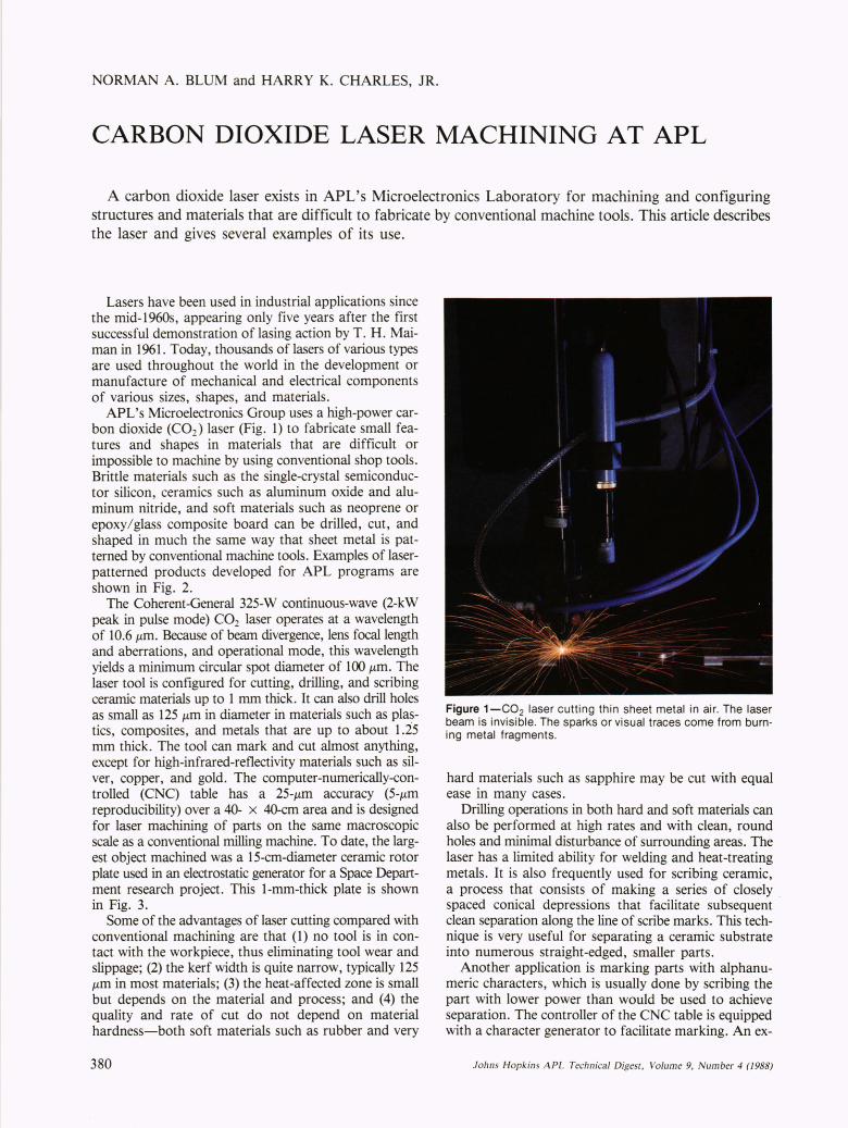
APL's Microelectronics Group uses a high-power carbon dioxide (C02) laser (Fig. 1) to fabricate small features and shapes in materials that are difficult or impossible to machine by using conventional shop tools. Brittle materials such as the single-crystal semiconductor silicon, ceramics such as aluminum oxide and aluminum nitride, and soft materials such as neoprene or epoxy/ glass composite board can be drilled, cut, and shaped in much the same way that sheet metal is patterned by conventional machine tools. Examples of laserpatterned products developed for APL programs are shown in Fig. 2.
The Coherent-General 325-W continuous-wave (2-kW peak in pulse mode) CO2 laser operates at a wavelength of 10.6 j-tm. Because of beam divergence, lens focal length and aberrations, and operational mode, this wavelength yields a minimum circular spot diameter of 100 j-tm. The laser tool is configured for cutting, drilling, and scribing ceramic materials up to 1 mm thick. It can also drill holes as small as 125 j-tm in diameter in materials such as plastics, composites, and metals that are up to about 1.25 mm thick. The tool can mark and cut almost anything, except for high-infrared-reflectivity materials such as silver, copper, and gold. The computer-numerically-controlled (CNC) table has a 25-j-tm accuracy (5-j-tm reproducibility) over a 40- x 4O-cm area and is designed for laser machining of parts on the same macroscopic scale as a conventional milling machine. To date, the largest object machined was a 15-cm-diameter ceramic rotor plate used in an electrostatic generator for a Space Department research project. This I-mm-thick plate is shown in Fig. 3.
Some of the advantages of laser cutting compared with conventional machining are that (1) no tool is in contact with the workpiece, thus eliminating tool wear and slippage; (2) the kerf width is quite narrow, typically 125 j-tm in most materials; (3) the heat-affected zone is small but depends on the material and process; and (4) the quality and rate of cut do not depend on material hardness-both soft materials such as rubber and very
380
Figure 1-C02 laser cutting thin sheet metal in air. The laser beam is invisible. The sparks or visual traces come from burning metal fragments.
hard materials such as sapphire may be cut with equal ease in many cases.
Drilling operations in both hard and soft materials can also be performed at high rates and with clean, round holes and minimal disturbance of surrounding areas. The laser has a limited ability for welding and heat-treating metals. It is also frequently used for scribing ceramic, a process that consists of making a series of closely spaced conical depressions that facilitate subsequent clean separation along the line of scribe marks. This technique is very useful for separating a ceramic substrate into numerous straight-edged, smaller parts.
Another application is marking parts with alphanumeric characters, which is usually done by scribing the part with lower power than would be used to achieve separation. The controller of the CNC table is equipped with a character generator to facilitate marking. An ex-
Johns Hopkins APL Technical Digest, Volume 9, Number 4 (1988)
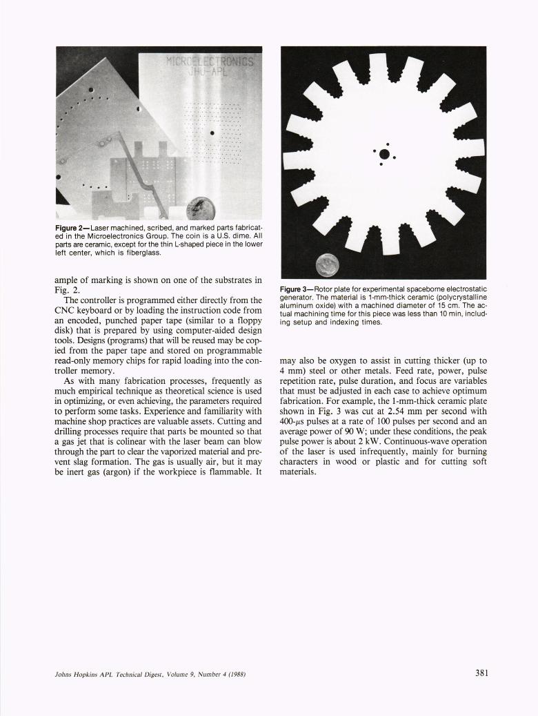
Figure 2-Laser machined, scribed, and marked parts fabricated in the Microelectronics Group. The coin is a U.S. dime. All parts are ceramic, except for the thin L-shaped piece in the lower left center, which is fiberglass.
ample of marking is shown on one of the substrates in Fig. 2.
The controller is programmed either directly from the CNC keyboard or by loading the instruction code from an encoded, punched paper tape (similar to a floppy disk) that is prepared by using computer-aided design tools. Designs (programs) that will be reused may be copied from the paper tape and stored on programmable read-only memory chips for rapid loading into the controller memory.
As with many fabrication processes, frequently as much empirical technique as theoretical science is used in optimizing, or even achieving, the parameters required to perform some tasks. Experience and familiarity with machine shop practices are valuable assets . Cutting and drilling processes require that parts be mounted so that a gas jet that is colinear with the laser beam can blow through the part to clear the vaporized material and prevent slag formation. The gas is usually air, but it may be inert gas (argon) if the workpiece is flammable. It
fohn s Hopkin s A PL Technical Digest, Volume 9, N umber 4 (1 988)
Figure 3-Rotor plate for experimental spaceborne electrostatic generator. The material is 1-mm-thick ceramic (polycrystalline aluminum oxide) with a machined diameter of 15 cm. The actual machining time for this piece was less than 10 min, including setup and indexing times.
may also be oxygen to assist in cutting thicker (up to 4 mm) steel or other metals. Feed rate, power, pulse repetition rate, pulse duration, and focus are variables that must be adjusted in each case to achieve optimum fabrication . For example, the I-mm-thick ceramic plate shown in Fig. 3 was cut at 2.54 mm per second with 400-j.ts pulses at a rate of 100 pulses per second and an average power of 90 W; under these conditions, the peak pulse power is about 2 kW. Continuous-wave operation of the laser is used infrequently, mainly for burning characters in wood or plastic and for cutting soft materials.
381
Blum, Charles - Carbon Dioxide Laser Machining at APL
THE AUTHORS
NORMAN A. BLUM is a member of APL's Principal Professional Staff. He has 25 years' experience in solid-state physics research, including thin fIlms, optical and magnetic properties of materials, Mossbauer spectroscopy, thin-film photovoltaics, and microelectronic processing. He has authored or coauthored more than 70 technical publications. Dr. Blum was educated at Harvard College, MIT, and Brandeis University, where he received a Ph.D. in physics in 1964. He did postdoctoral work and was a staff member at the MIT Francis Bitter National Magnet Laboratory from
1960 to 1966 and was a senior staff physicist at the NASA Electronics Research Center in Cambridge, Mass., from 1966 to 1970. He then joined the Milton S. Eisenhower Research Center at APL as a staff physicist, a position he held until 1984. Since then, he has been section supervisor of the Substrate Processing Section in APL's Microelectronics Group. He is a member of several professional societies and last year served on the Presidential Awards Selection Board to choose the national recipients of the Presidential Outstanding Science Teacher Awards.
382
HARRY K. CHARLES, Jr., is a member of APL's Principal Professional Staff and is an engineer and the supervisor of the Microelectronics Group. He has been actively engaged in microelectronic research and advanced packaging development for over 12 years. Current technical interests include the study of contacts and interfacial phenomena in hybrids and surface-mounted microelectronic assemblies, and the development of a graduate curriculum for microelectronic packaging education. He has published more than 85 technical papers.
Dr. Charles received a B.S.E.E. degree from Drexel University in 1967 and a Ph.D. degree in electrical engineering from The Johns Hopkins University in 1972. After completing a postdoctoral research appointment at APL, he joined the Microelectronics Group.
He is a senior member of the IEEE and a member of the Components, Hybrids and Manufacturing Technology (CHMT) Society, the Electron Devices Society, and the Education Society. He is a member of the CHMT Ad Comm, where he is serving as Standards Committee Chairman. He is also a member of the American Physical Society and the International Society for Hybrid Microelectronics. Dr. Charles has been listed for several years in Who's Who in the East, American Men and Women oj Science, the Dictionary oj International Biography, Men oj Achievement, and Who 's Who in Technology Today.
John s Hopkins APL Technical Digest, Volume 9, Number 4 (/988)