Bidirectional Isolated DC/DC Converter with Wide Input Voltage Range for Residential Energy Management Applications Ralph M. Burkart and J. W. Kolar Swiss Federal Institute of Technology (ETH) Zurich Power Electronic Systems Laboratory www.pes.ee.ethz.ch Case Study
Transcript
1/xy
Bidirectional Isolated DC/DC Converter with Wide Input Voltage Range
for Residential Energy Management ApplicationsRalph M. Burkart and J. W. Kolar
Swiss Federal Institute of Technology (ETH) ZurichPower Electronic Systems Laboratory
www.pes.ee.ethz.ch
Case Study
2/17
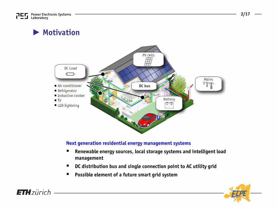
Motivation
Next generation residential energy management systems
Renewable energy sources, local storage systems and intelligent load management
DC distribution bus and single connection point to AC utility grid
Possible element of a future smart grid system
3/17
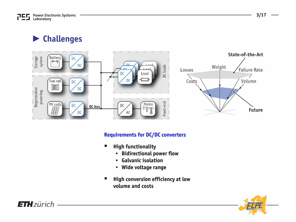
Challenges
Requirements for DC/DC converters
High functionality• Bidirectional power flow• Galvanic isolation• Wide voltage range
High conversion efficiency at low volume and costs
4/17
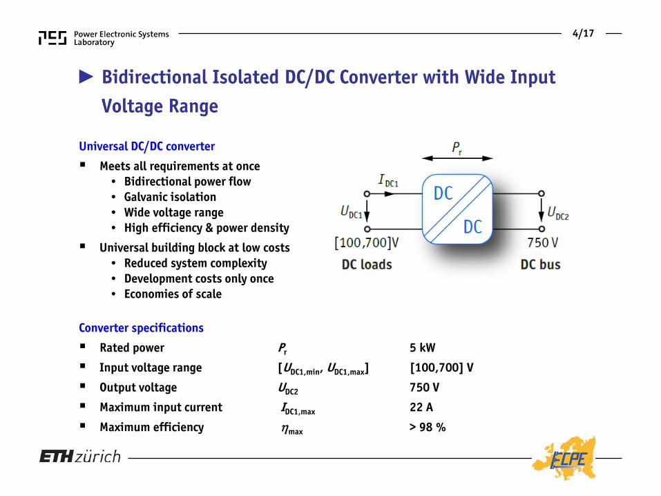
Bidirectional Isolated DC/DC Converter with Wide Input Voltage Range
Universal DC/DC converter
Meets all requirements at once• Bidirectional power flow• Galvanic isolation• Wide voltage range• High efficiency & power density
Universal building block at low costs• Reduced system complexity• Development costs only once• Economies of scale
Converter specifications
Rated power Pr 5 kW
Input voltage range [UDC1,min, UDC1,max] [100,700] V
Output voltage UDC2 750 V
Maximum input current IDC1,max 22 A
Maximum efficiency ηmax > 98 %
5/17
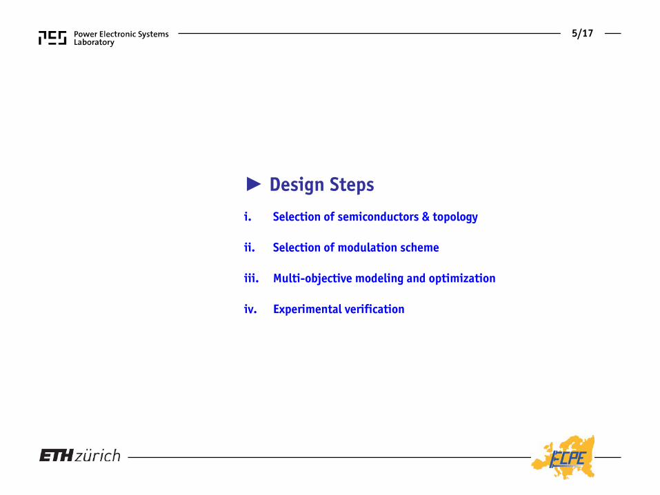
Design Stepsi. Selection of semiconductors & topology
ii. Selection of modulation scheme
iii. Multi-objective modeling and optimization
iv. Experimental verification
6/17
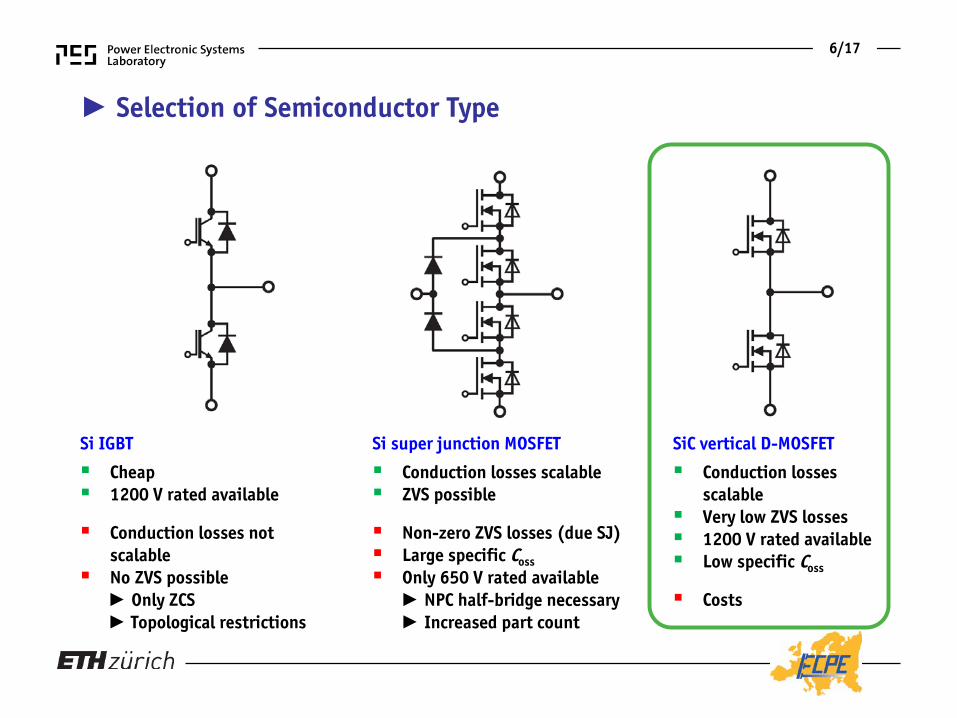
Selection of Semiconductor Type
Si IGBT
Cheap 1200 V rated available
Conduction losses not scalable
No ZVS possible Only ZCS Topological restrictions
Si super junction MOSFET
Conduction losses scalable ZVS possible
Non-zero ZVS losses (due SJ) Large specific Coss Only 650 V rated available
NPC half-bridge necessary Increased part count
SiC vertical D-MOSFET
Conduction losses scalable
Very low ZVS losses 1200 V rated available Low specific Coss
Costs
7/17
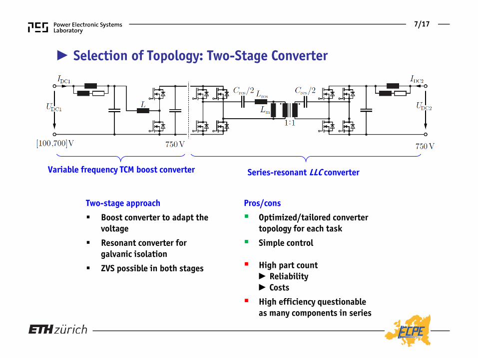
Selection of Topology: Two-Stage Converter
Two-stage approach
Boost converter to adapt the voltage
Resonant converter for galvanic isolation
ZVS possible in both stages
Pros/cons
Optimized/tailored converter topology for each task
Simple control
High part count Reliability Costs
High efficiency questionable as many components in series
Variable frequency TCM boost converter Series-resonant LLC converter
8/17
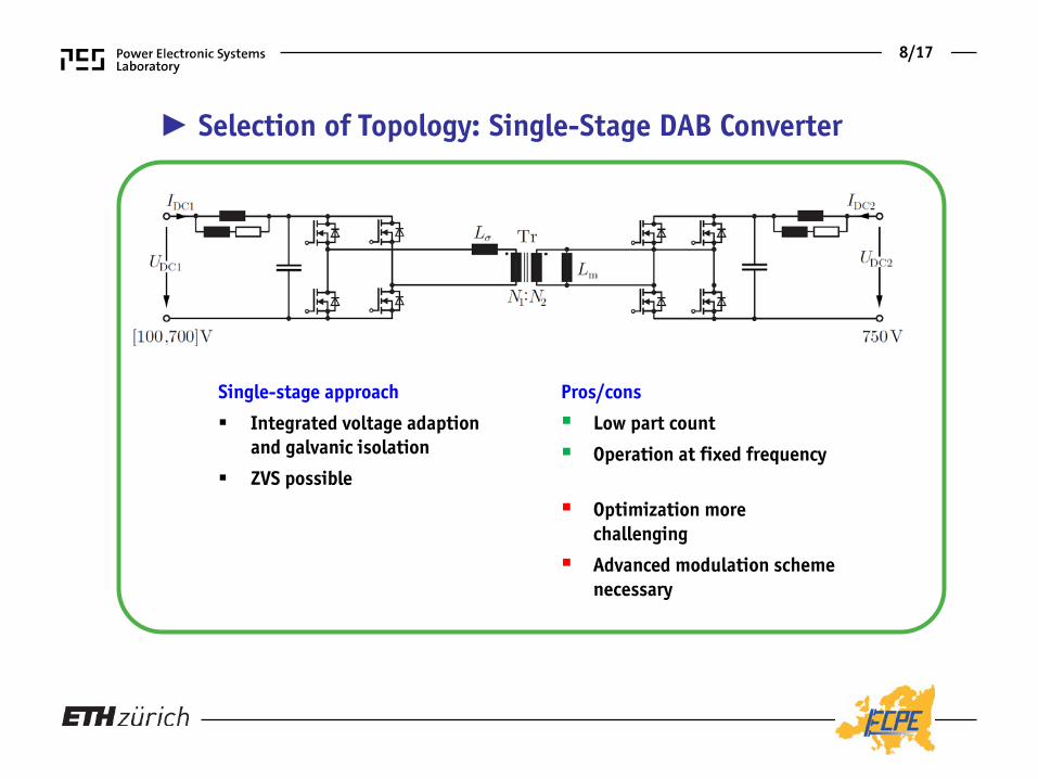
Selection of Topology: Single-Stage DAB Converter
Single-stage approach
Integrated voltage adaption and galvanic isolation
ZVS possible
Pros/cons
Low part count
Operation at fixed frequency
Optimization more challenging
Advanced modulation scheme necessary
9/17
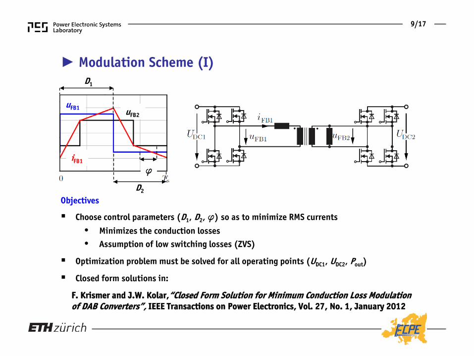
Modulation Scheme (I)
Objectives
Choose control parameters (D1, D2, ϕ) so as to minimize RMS currents• Minimizes the conduction losses• Assumption of low switching losses (ZVS)
Optimization problem must be solved for all operating points (UDC1, UDC2, Pout)
Closed form solutions in:
F. Krismer and J.W. Kolar,“Closed Form Solution for Minimum Conduction Loss Modulation of DAB Converters”, IEEE Transactions on Power Electronics, Vol. 27, No. 1, January 2012
D1
D2
ϕ
uFB1 uFB2
iFB1
10/17
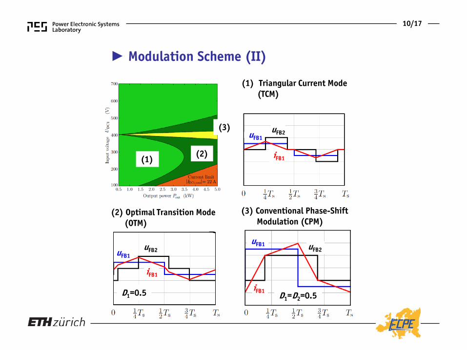
Modulation Scheme (II)
(1) Triangular Current Mode(TCM)
uFB1uFB2
iFB1(1)
(2) Optimal Transition Mode (OTM)
uFB1uFB2
iFB1
D1=0.5
(2)
(3) Conventional Phase-ShiftModulation (CPM)
uFB1 uFB2
iFB1 D1=D2=0.5
(3)
11/17
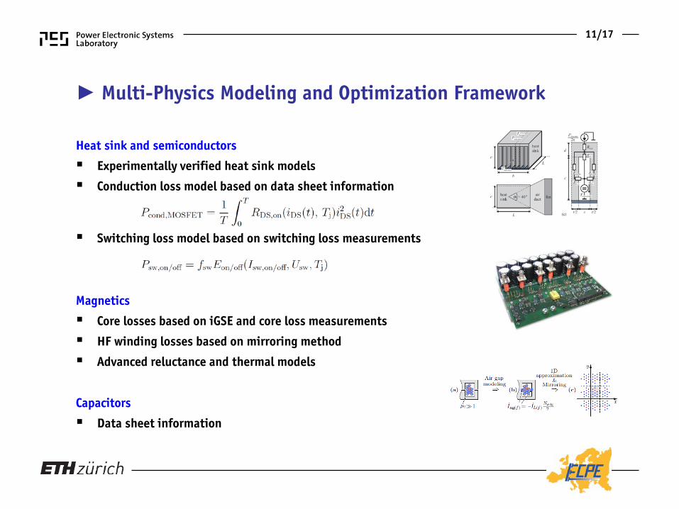
Multi-Physics Modeling and Optimization Framework
Heat sink and semiconductors
Experimentally verified heat sink models
Conduction loss model based on data sheet information
Switching loss model based on switching loss measurements
Magnetics
Core losses based on iGSE and core loss measurements
HF winding losses based on mirroring method
Advanced reluctance and thermal models
Capacitors
Data sheet information
12/17
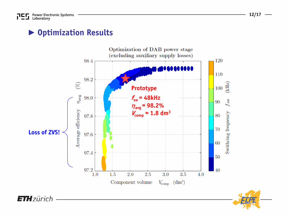
Optimization Results
Prototype
fsw = 48kHzηavg = 98.2%Vcomp = 1.8 dm3
Loss of ZVS!
13/17
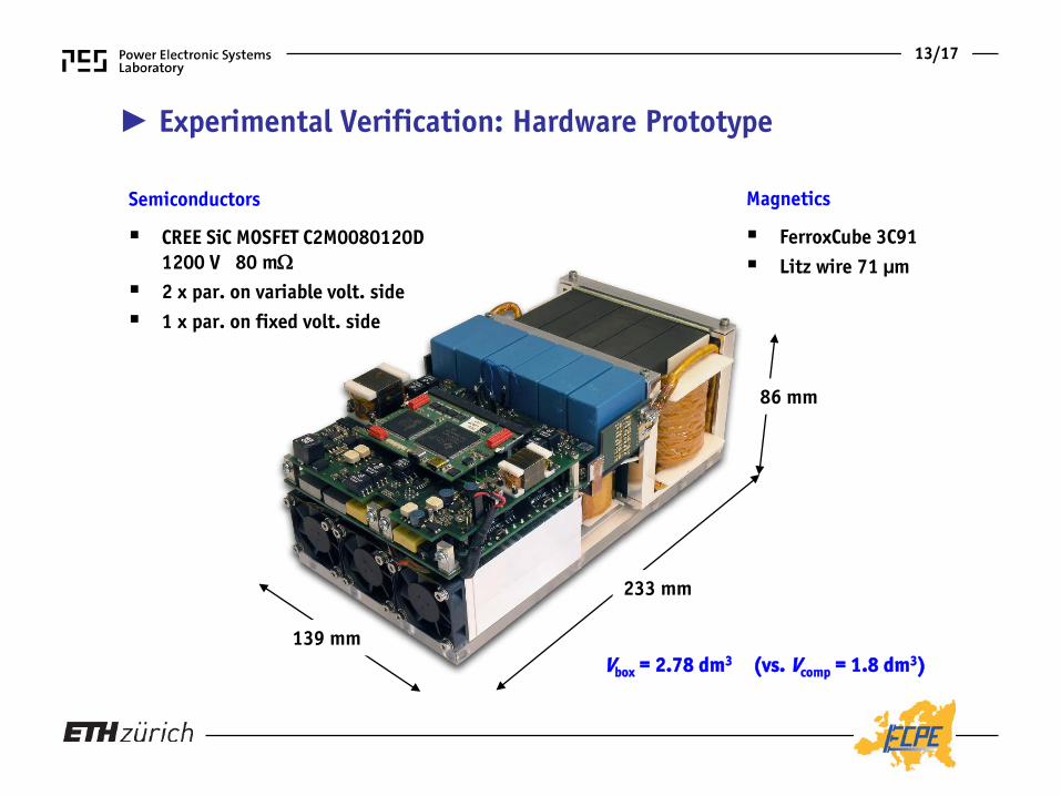
Experimental Verification: Hardware Prototype
233 mm
86 mm
139 mmVbox = 2.78 dm3 (vs. Vcomp = 1.8 dm3)
Semiconductors
CREE SiC MOSFET C2M0080120D 1200 V 80 mΩ
2 x par. on variable volt. side 1 x par. on fixed volt. side
Magnetics
FerroxCube 3C91 Litz wire 71 µm
14/17
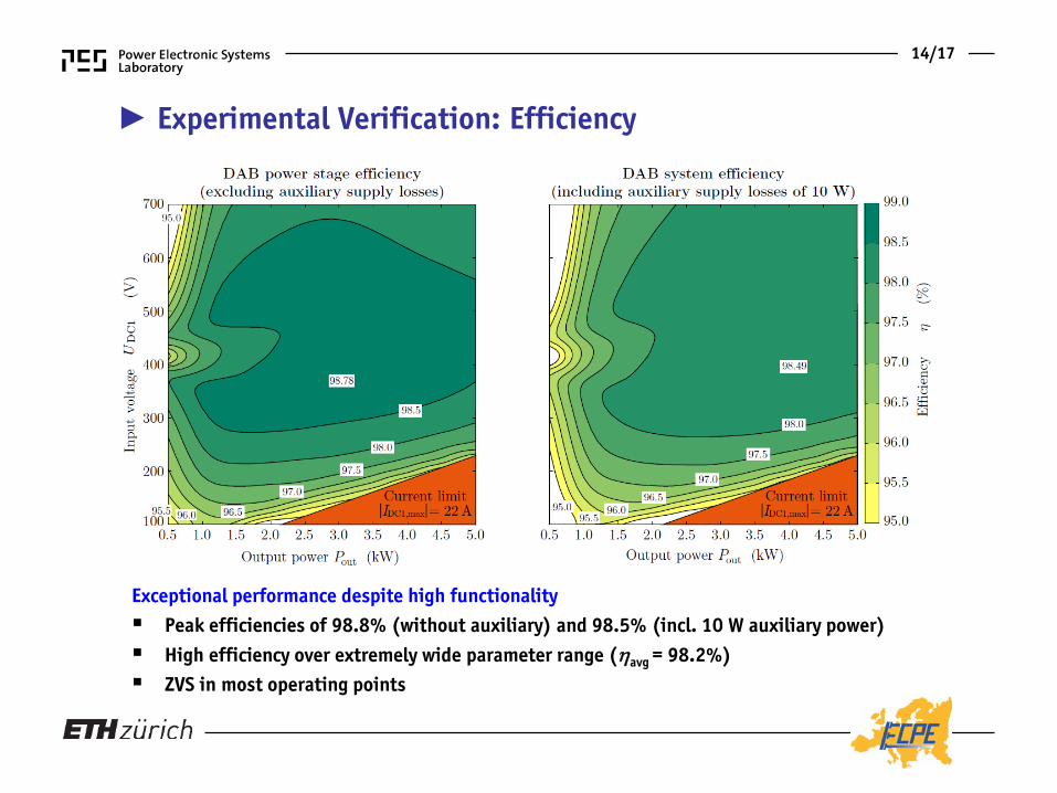
Experimental Verification: Efficiency
Exceptional performance despite high functionality Peak efficiencies of 98.8% (without auxiliary) and 98.5% (incl. 10 W auxiliary power) High efficiency over extremely wide parameter range (ηavg = 98.2%) ZVS in most operating points
15/17
Experimental Verification: Power Density
Definition of power density Power density only meaningful in combination with specification of
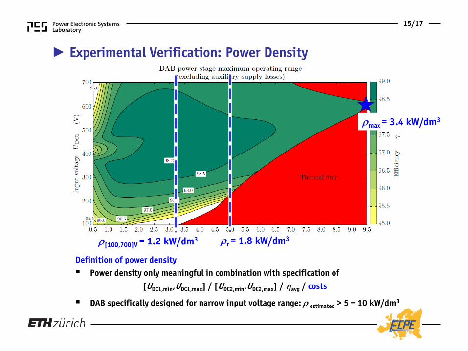
![BIDIRECTIONAL DC-to-DC CONVERTER WITH · PDF fileBIDIRECTIONAL DC-to-DC CONVERTER WITH EXTENDED VOLTAGE TRANSFER RATIO ... well-known push-pull converter [3] ... IRF840 (S3 &](https://static.documents.pub/doc/80x56/5abe38867f8b9a3a428cb169/bidirectional-dc-to-dc-converter-with-dc-to-dc-converter-with-extended-voltage.jpg)


