Xi'an Jiaotong-Liverpool University Department of Electrical and Electronic Engineering Sustainable Energy Technologies Laboratory Master’s Thesis Defense Presentation 2013 December 11 The Bidirectional Dual Active Bridge DC/DC Converter for Photovoltaic Application Wenlong JING Supervisor : Dr. Huiqing WEN
Transcript
Xi'an Jiaotong-Liverpool University
Department of Electrical and Electronic Engineering
Sustainable Energy Technologies Laboratory
Master’s Thesis Defense Presentation
2013 December 11
The Bidirectional Dual Active
Bridge DC/DC Converter for
Photovoltaic Application
Wenlong JING
Supervisor : Dr. Huiqing WEN
1
Presentation Overview
Introduction
Theoretical Analysis
PSIM Simulation
Prototype Design
Experiments
Conclusions
Reference
Acknowledgements
Master’s Thesis Defense Presentation
2
Chapter 1
Introduction
Thesis Background
Bidirectional DC/DC Converter (BDC)
Bidirectional DAB DC/DC Converter (BDC-DAB)
Thesis Objectives
Master’s Thesis Defense Presentation
3
Introduction Thesis Background
Energy Crisis : Another 41 years
Solution: Renewable Energy
Drawback: Randomness, Unpredictability and Intermittent
World Market Energy Use by Energy Type [1]
Master’s Thesis Defense Presentation
[1] Maureen Lorenzetti, “BP: World oil and gas reserves still growing at healthy pace” Oil and gas journal, June 2004.
4
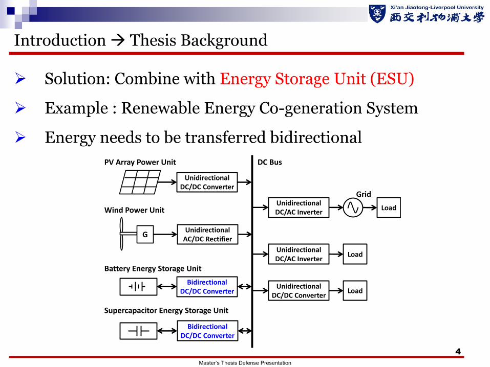
Introduction Thesis Background
Solution: Combine with Energy Storage Unit (ESU)
Example : Renewable Energy Co-generation System
Energy needs to be transferred bidirectional
Unidirectional DC/DC Converter
Load
Unidirectional AC/DC Rectifier
Bidirectional DC/DC Converter
Bidirectional DC/DC Converter
Unidirectional DC/AC Inverter
Unidirectional DC/DC Converter
Unidirectional DC/AC Inverter
Load
Load
G
DC BusPV Array Power Unit
Wind Power Unit
Battery Energy Storage Unit
Supercapacitor Energy Storage Unit
Grid
Master’s Thesis Defense Presentation
5
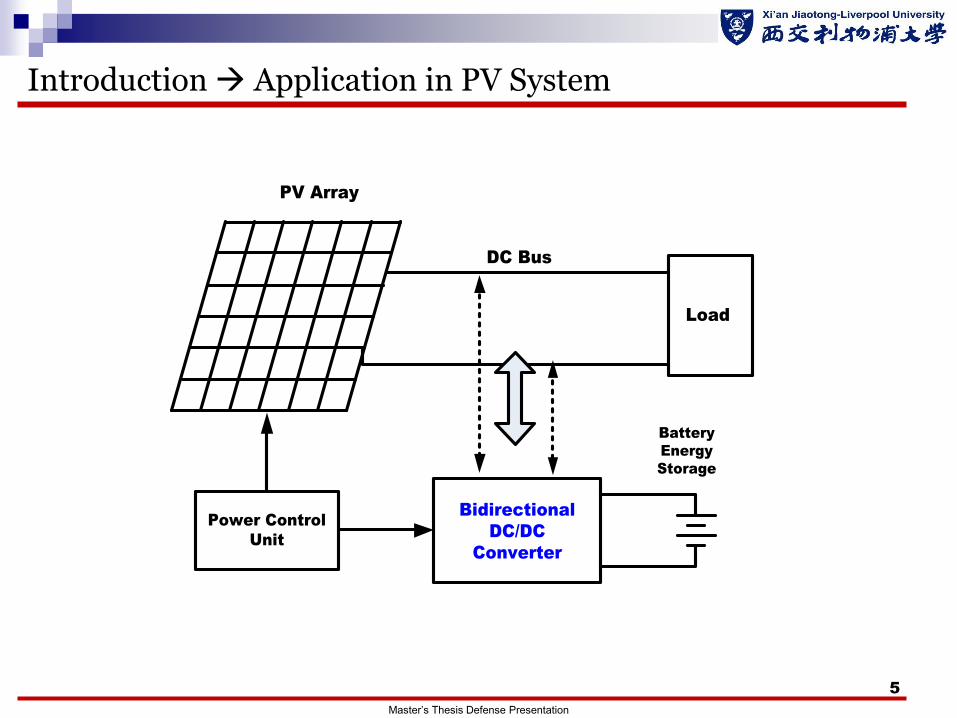
Introduction Application in PV System
Load
Bidirectional
DC/DC
Converter
DC Bus
Power Control
Unit
Battery
Energy
Storage
PV Array
Master’s Thesis Defense Presentation
6
Introduction BDC
Bidirectional DC/DC Converter (BDC) :
DC voltage polarity : Same and Unchanged
Energy : Bidirectional Transmission
Stabilized Voltage and Current
Two Operation Modes : Forward & Reverse Mode
Bidirectional DC/DC Converter
Forward mode
Reverse mode
>0 , <0
<0 , >0
Master’s Thesis Defense Presentation
7
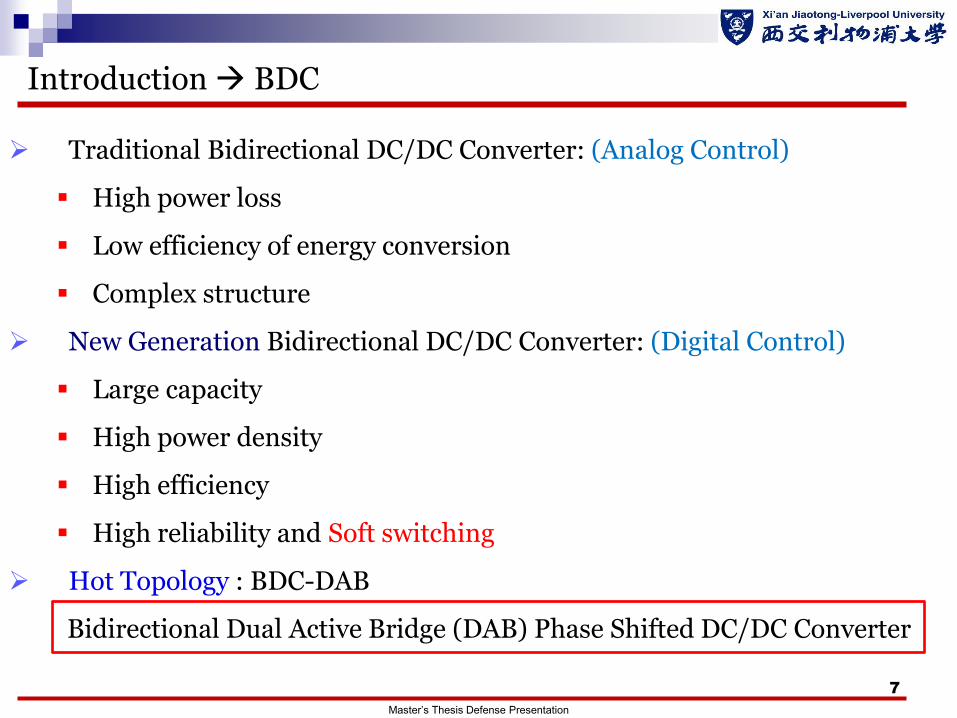
Introduction BDC
Traditional Bidirectional DC/DC Converter: (Analog Control)
High power loss
Low efficiency of energy conversion
Complex structure
New Generation Bidirectional DC/DC Converter: (Digital Control)
Large capacity
High power density
High efficiency
High reliability and Soft switching
Hot Topology : BDC-DAB
Bidirectional Dual Active Bridge (DAB) Phase Shifted DC/DC Converter
Master’s Thesis Defense Presentation
8
Introduction Soft Switching
1. Zero Voltage Switching (ZVS)
When the switch on or off :
The voltage of switch is zero.
2. Zero Current Switching (ZCS)
When the switch on or off :
The current flow is zero.
Reduce switching losses and Improve efficiency
Contain a pair of the resonant inductor and capacitor
Master’s Thesis Defense Presentation
9
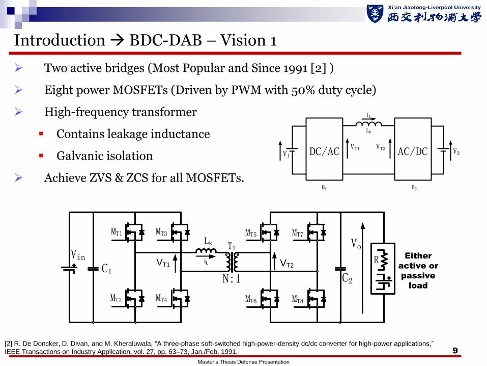
Introduction BDC-DAB – Vision 1
Two active bridges (Most Popular and Since 1991 [2] )
Eight power MOSFETs (Driven by PWM with 50% duty cycle)
High-frequency transformer
Contains leakage inductance
Galvanic isolation
Achieve ZVS & ZCS for all MOSFETs.
MT1
C1
MT3
MT2 MT4
N:1
MT5 MT7
MT6 MT8
Lk
VinT1
R Either
active or
passive
load
iLVT1 VT2
C2
Vo
Master’s Thesis Defense Presentation
[2] R. De Doncker, D. Divan, and M. Kheraluwala, “A three-phase soft-switched high-power-density dc/dc converter for high-power applications,”
IEEE Transactions on Industry Application, vol. 27, pp. 63–73, Jan./Feb. 1991.
DC/AC AC/DC
iL
VT1 VT2
B1 B2
V1 V2
Lk
10
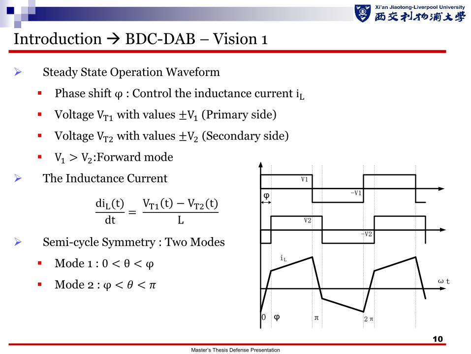
Introduction BDC-DAB – Vision 1
V1
-V1
V2
-V2
0 π 2π
φ
ωt
φ
iL
Steady State Operation Waveform
Phase shift φ : Control the inductance current iL
Voltage VT1 with values ±V1 (Primary side)
Voltage VT2 with values ±V2 (Secondary side)
V1 > V2:Forward mode
The Inductance Current
Semi-cycle Symmetry : Two Modes
Mode 1 : 0 < θ < φ
Mode 2 : φ < 𝜃 < 𝜋
diL(t)
dt= VT1 t − VT2(t)
L
Master’s Thesis Defense Presentation
11
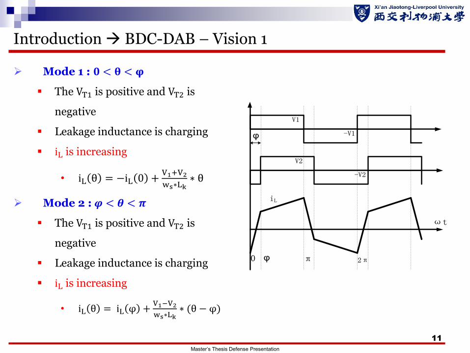
Introduction BDC-DAB – Vision 1
V1
-V1
V2
-V2
0 π 2π
φ
ωt
φ
iL
Mode 1 : 𝟎 < 𝛉 < 𝛗
The VT1 is positive and VT2 is
negative
Leakage inductance is charging
iL is increasing
• iL θ = −iL 0 +V1+V2
ws∗Lk∗ θ
Mode 2 : 𝝋 < 𝜽 < 𝝅
The VT1 is positive and VT2 is
negative
Leakage inductance is charging
iL is increasing
• iL θ = iL φ +V1−V2
ws∗Lk∗ (θ − φ)
Master’s Thesis Defense Presentation
12
Introduction BDC-DAB – Vision 1
Main Problem : The energy circulates from output to input with a quite
significant value
Causes high conduction losses
Reach 25% of the total output power at maximum output power
Cause high current ripple at the output filter capacitors
Reduces the efficiency
Motivation
Explore a DAB DC/DC converter to overcome the problem
Still keep the original features
Improve the efficiency
Master’s Thesis Defense Presentation
13
Introduction Thesis Objectives
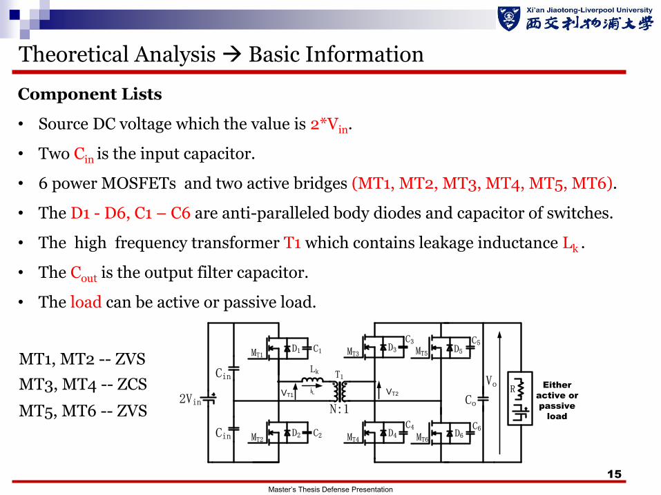
Proposed a different vision of Bidirectional DAB DC/DC Converter [3]
High Frequency Transformer with Leakage Inductance
Half bridge in the primary side (Two MOSFETs)
The circulation energy can be eliminated effectively
Total 6 MOSFETs : Reduce the complexity of the control scheme
Cin
N:1
Lk
2Vin
T1
R Either
active or
passive
load
iLVT1 VT2
Co
VoCin
MT1D1 C1 MT5 D5
C5
MT2D2 C2
MT3D3
C3
MT4D4
C4MT6
D6C6
Master’s Thesis Defense Presentation
[3] Zhang, J.M.; Xu, D.M.; Zhaoming Qian, "An improved dual active bridge DC/DC converter," Power Electronics Specialists
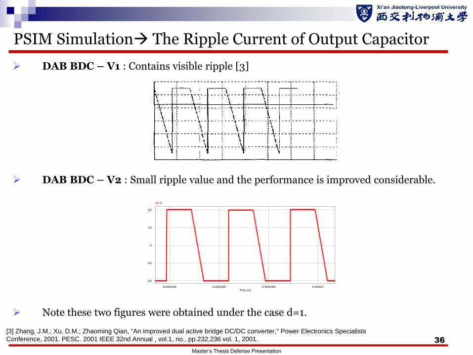
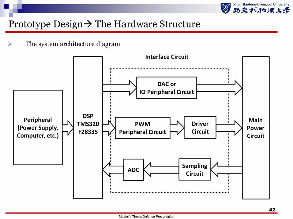
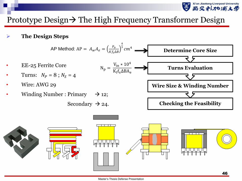
Prototype Design The High Frequency Transformer Design
Checking the Feasibility
Wire Size & Winding Number
Turns Evaluation
Determine Core Size AP Method: AP = 𝐴𝑤𝐴𝑒 =𝑃𝑜
𝐾𝑓𝑠∆𝐵
4
3𝑐𝑚4
Np = Vin ∗ 10
4
Kffs∆BAe
Master’s Thesis Defense Presentation
47
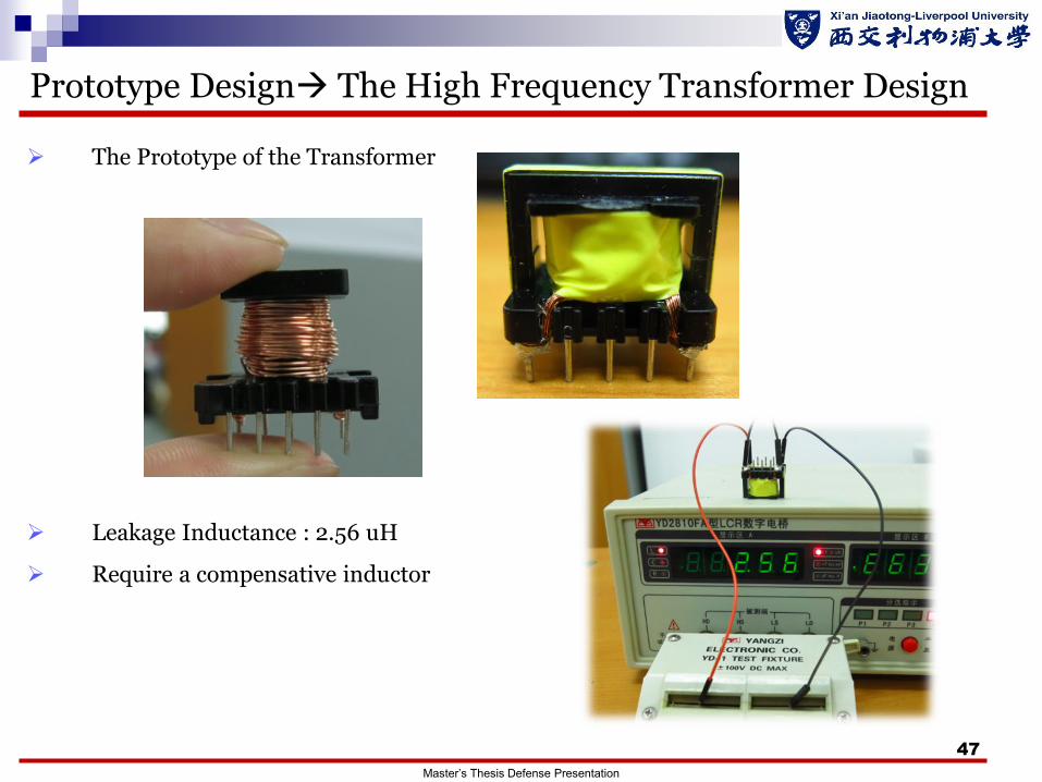
The Prototype of the Transformer
Leakage Inductance : 2.56 uH
Require a compensative inductor
Prototype Design The High Frequency Transformer Design
Master’s Thesis Defense Presentation
48
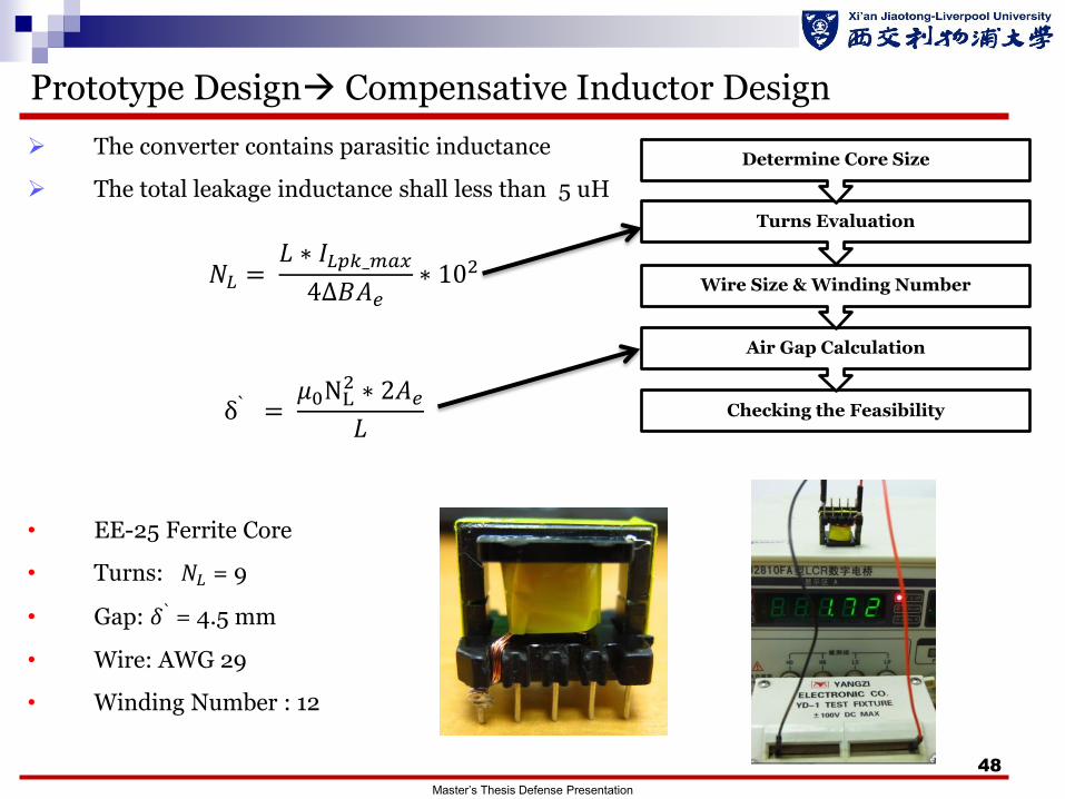
The converter contains parasitic inductance
The total leakage inductance shall less than 5 uH
• EE-25 Ferrite Core
• Turns: 𝑁𝐿 = 9
• Gap: 𝛿 ` = 4.5 mm
• Wire: AWG 29
• Winding Number : 12
Prototype Design Compensative Inductor Design
Checking the Feasibility
Air Gap Calculation
Wire Size & Winding Number
Turns Evaluation
Determine Core Size
𝑁𝐿 = 𝐿 ∗ 𝐼𝐿𝑝𝑘_𝑚𝑎𝑥4∆𝐵𝐴𝑒
∗ 102
δ` = 𝜇0NL
2 ∗ 2𝐴𝑒𝐿
Master’s Thesis Defense Presentation
49
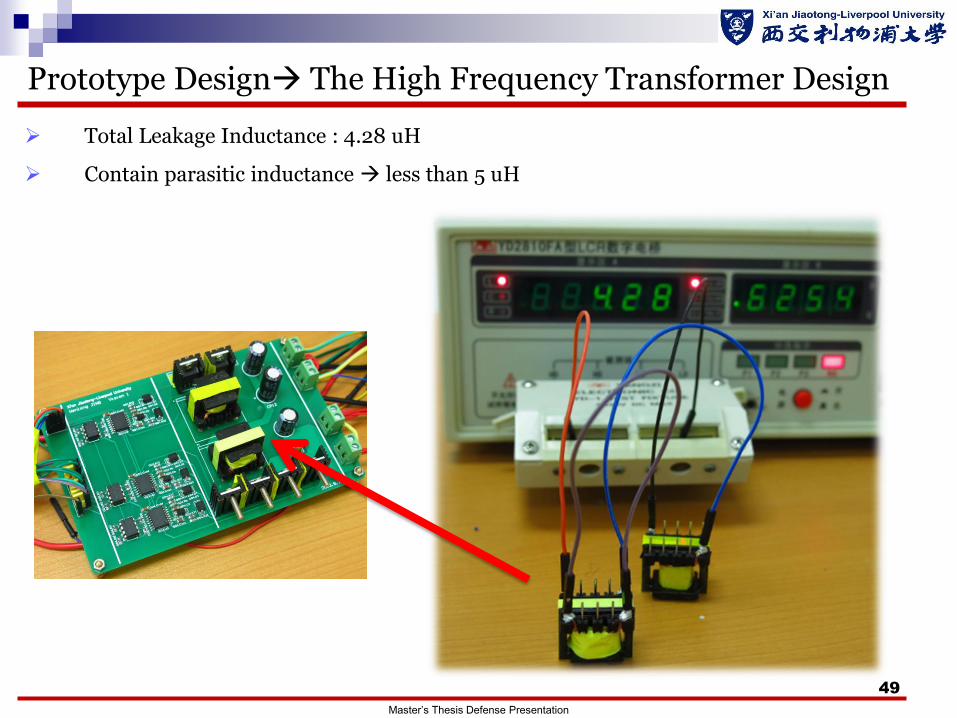
Prototype Design The High Frequency Transformer Design
Total Leakage Inductance : 4.28 uH
Contain parasitic inductance less than 5 uH
Master’s Thesis Defense Presentation
50
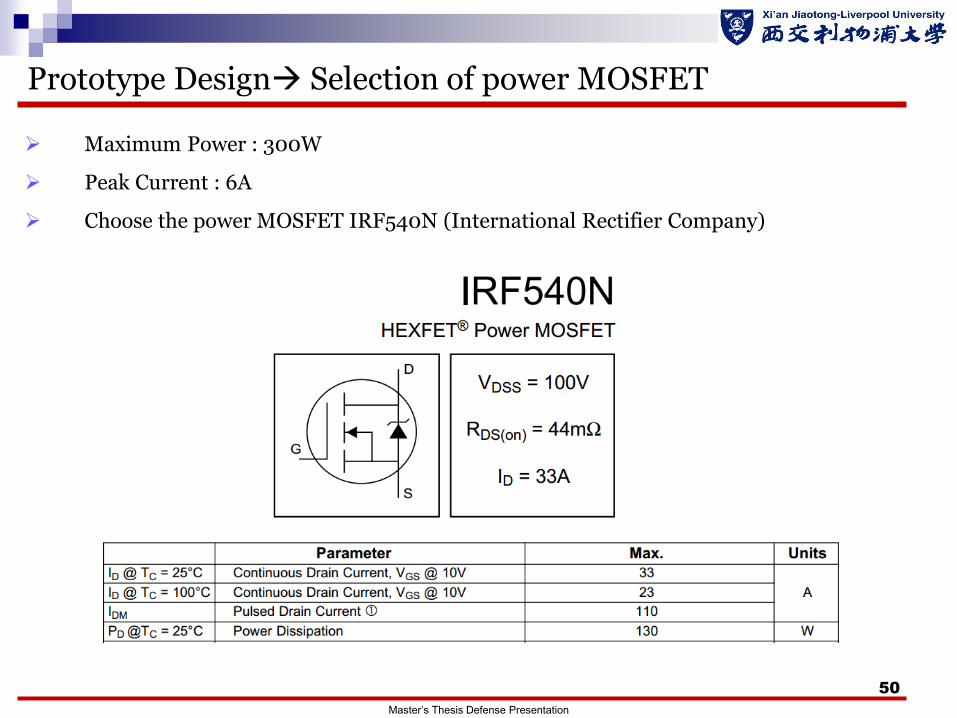
Maximum Power : 300W
Peak Current : 6A
Choose the power MOSFET IRF540N (International Rectifier Company)
Prototype Design Selection of power MOSFET
Master’s Thesis Defense Presentation
51
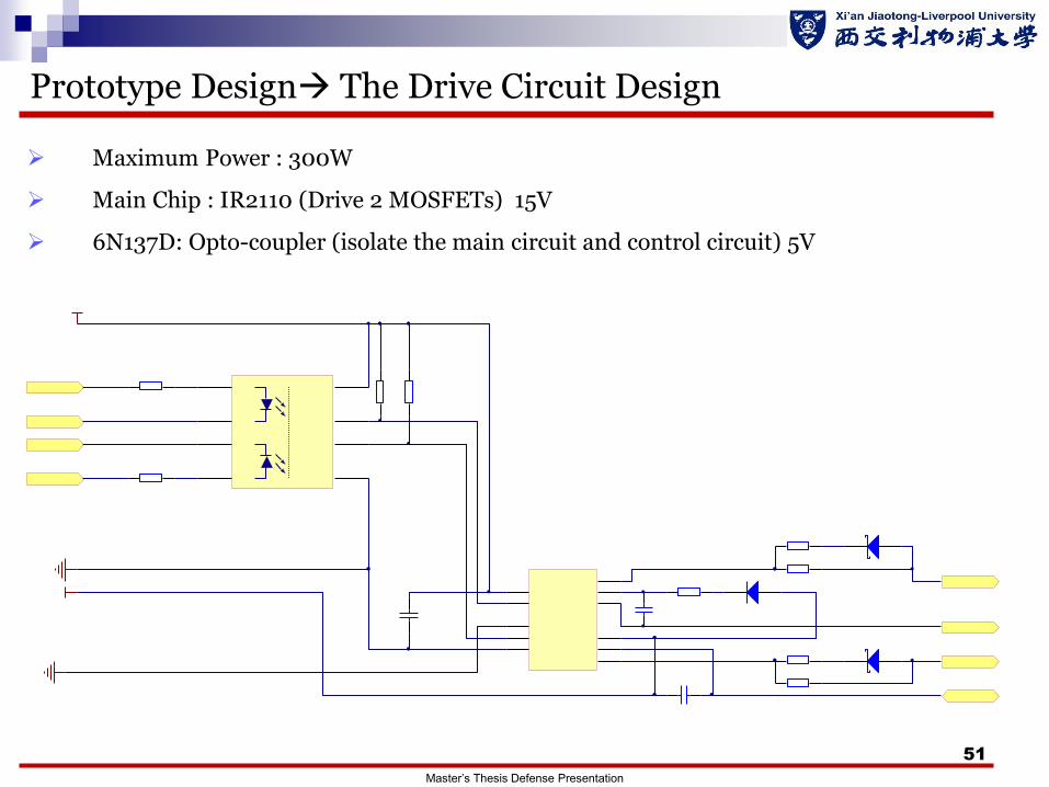
Maximum Power : 300W
Main Chip : IR2110 (Drive 2 MOSFETs) 15V
6N137D: Opto-coupler (isolate the main circuit and control circuit) 5V
Prototype Design The Drive Circuit Design
L O
1
C O M
2
V C C
3
V S
6
V B
7
H O
8
V D D
1 1
HIN
1 2
S D
1 3
LIN
1 4
VSS
1 5
U D
IRS2110
D b
Diode FRD
G D H
G D L
1 K
R b
3 3 0 n F
C b
3 3 0 n F
Cvdd
M P
C O M
3 3 0 n F
Cvcc
6 o h m
R12
6 6 o h m
R11
D 1
D Schottky
6 o h m
R22
6 6 o h m
R21
D 2
D Schottky
+
-
V C C
Vout1
Vout2
G N D+
-
Vf1
Vf2
U101
6N137D
4 7 0 o h m
RI1
4 7 0 o h m
R O 1
4 7 0 o h m
R O 2
4 7 0 o h m
RI2
HIN-
LIN-
HIN+
LIN+
V D D
VSS
V C C
S D
Master’s Thesis Defense Presentation
52
Three Drive Signals
Drive 1 Drive 2
Drive 3
Master’s Thesis Defense Presentation
Prototype Design The Drive Circuit Design
53
Schematic Diagram
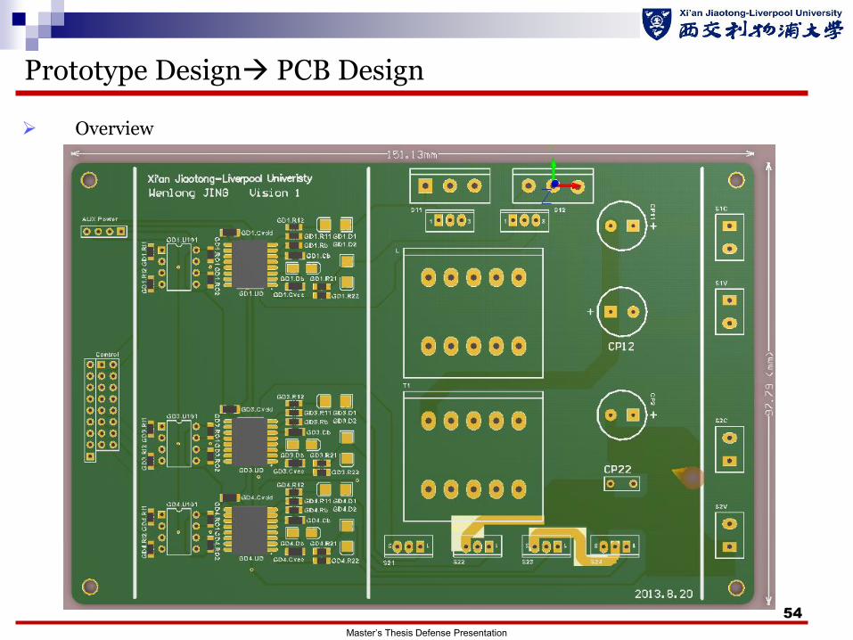
Prototype Design PCB Design
1 2
3 4
5 6
7 8
9 1 0
1 1 1 2
1 3 1 4
1 5 1 6
Control
S1H+ S1H-
S1L+ S1L-
S2H+
S2L+
S3H+
S3L+
S4H+
S4L+
S2H-
S2L-
S3H-
S3L-
S4H-
S4L-
1
2
3
4
AUX Power V D D
VSS
V C C
S D
1
2
3
4
5
6
7
8
9
C_VDD C V D D
S 1 1
IRF540
S 1 2
IRF540
T 1
Trans Eq
S 2 1
IRF540
S 2 2
IRF540
S 2 3
IRF540
S 2 4
IRF540
5 u H
L
Inductor Iron
G11
G12
G21
G22
G23
G24
1
2
S 1 V
100uF/ 100V
CP11
100uF/100V
CP2
M11
M12
M21
M22
P S 1 +
P S 1 - P S 2 -
P S 2 +
1
2
S 1 C
1
2
S 2 C
1
2
S 2 V
100uF 100V
CP12
0.01uF
CP22
HIN+
LIN+
G D H
G D L
M P
C O M
HIN-
LIN-
G D 1 Driver.SchDoc
S1H+
S1H-
S1L+
S1L-
G11
G12
M11
P S 1 -
Master’s Thesis Defense Presentation
54
Overview
Prototype Design PCB Design
Master’s Thesis Defense Presentation
55
The Microcontroller : DSP TMS320LF28335
The Features:
32-bit floating point CPU (150 MHz, modified Harvard architecture)
Memory: 68k SARAM, 512k Flash
MAC Operations
16 12-bit ADC Channels (25 MHz)
18 PWM Outputs
Low Power Dissipation
3 32-bit CPU Timers
1 Watchdog Timer
88 GPIO
6 Channel DMA
Prototype Design Software Design DSP
Master’s Thesis Defense Presentation
56
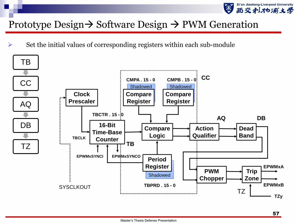
6 MOSFETs need three pairs of complementary PWM signals
PWM is a scheme to represent a signal as a sequence of pulses
Use ePWM Module in DSP to generate PWM
Two outputs : EPWMxA and EPWMxB
7 Sub-modules
Prototype Design Software Design PWM Generation
To power
switching
device
Power
supply rail
Gate signals are
complementary PWM
Time-base (TB) module
Counter-compare (CC) module
Action-qualifier (AQ) module
Dead-band (DB) module
Event-trigger (ET) module
Trip-zone (TZ) module
PWM-chopper (PC) module
ePWM module
GPIOMUX
EPWMxA
EPWMxB
EPWMxSYNCI
EPWMxSYNCO
PIE
ADC
EPWMxSOCA
EPWMxSOCB
Peripheral bus
to
Master’s Thesis Defense Presentation
57
Set the initial values of corresponding registers within each sub-module
Prototype Design Software Design PWM Generation
Compare
Logic
Action
Qualifier
Shadowed
Compare
Register
Shadowed
Clock
Prescaler
Shadowed
Compare
Register
CMPA . 15 - 0 CMPB . 15 - 0
EPWMxA
EPWMxBSYSCLKOUT
TZy
EPWMxSYNCI EPWMxSYNCO
TBCLK
TBCTR . 15 - 0
16-Bit
Time-Base
Counter
Dead
Band
Period
RegisterPWM
Chopper
Trip
ZoneTBPRD . 15 - 0
TB
CC
AQ DB
TB
CC
AQ
DB
TZ
TZ
Master’s Thesis Defense Presentation
58
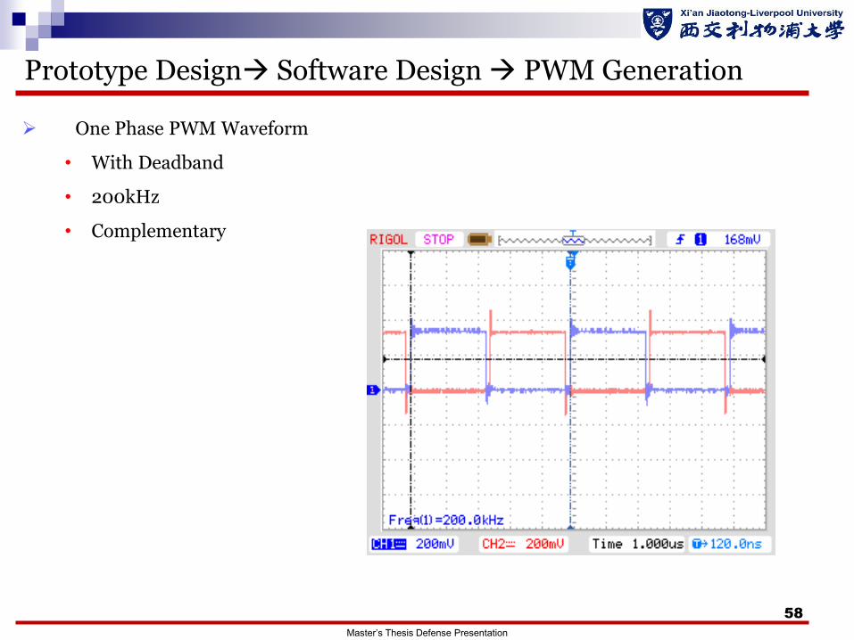
One Phase PWM Waveform
• With Deadband
• 200kHz
• Complementary
Prototype Design Software Design PWM Generation
Master’s Thesis Defense Presentation
SyncIn
SyncOut
CTR=zero
CTR=CMPB X
En
o o
o
o
o
o o =36° Phase
EPWM2A
EPWM2B
SyncIn
SyncOut
CTR=zero CTR=CMPB
X
En
o o
o
o
o
o o =72° Phase
EPWM3A
EPWM3B
SyncIn
SyncOut
CTR=zero
CTR=CMPB X
En
o o
o
o
o
o o =0° Phase
EPWM1A
EPWM1B
=36°
=72°
Prototype Design Software Design PWM Generation
59
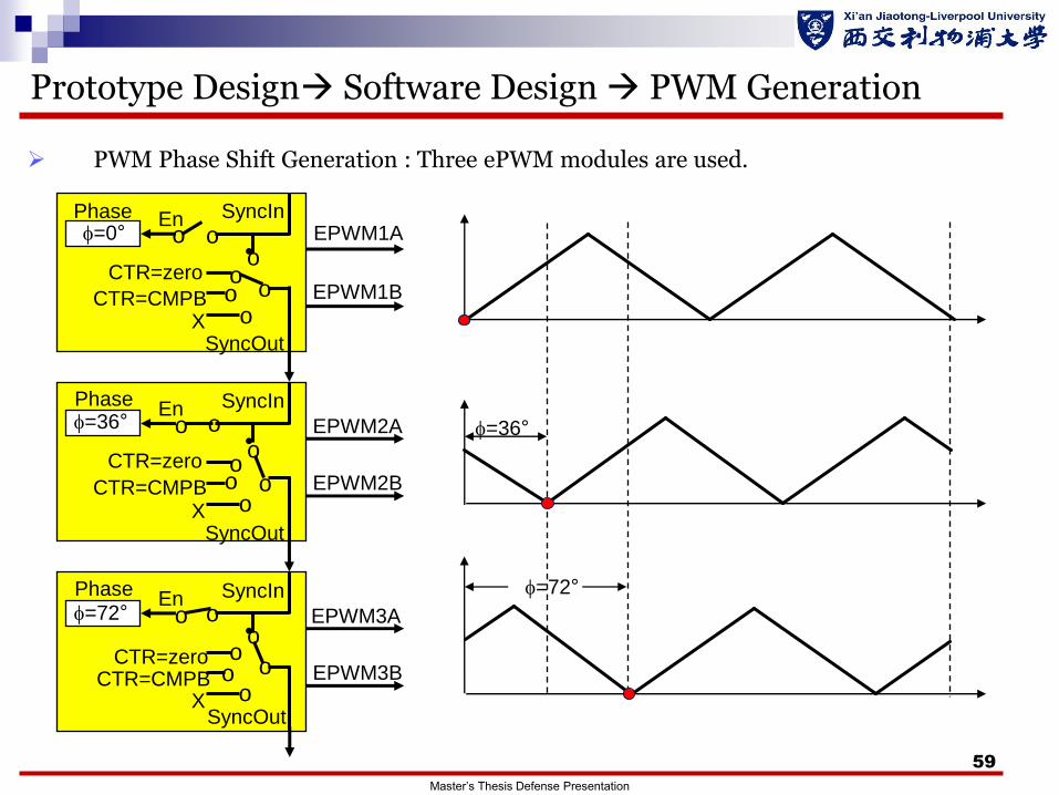
PWM Phase Shift Generation : Three ePWM modules are used.
Master’s Thesis Defense Presentation
60
Three pairs of complementary PWM signals
Prototype Design Software Design PWM Generation
MT1_MT3 MT1_MT5 MT3_MT6
Cin
N:1
Lk
2Vin
T1
R Either
active or
passive
load
iLVT1 VT2
Co
VoCin
MT1D1 C1 MT5 D5
C5
MT2D2 C2
MT3D3
C3
MT4D4
C4MT6
D6C6
Master’s Thesis Defense Presentation
61
Experiments
Basic Information
Drive Voltage of MOSFETs
The Transformer Current (Primary Side)
Soft Switching Condition Verification
Limitations
Chapter 5
Master’s Thesis Defense Presentation
62
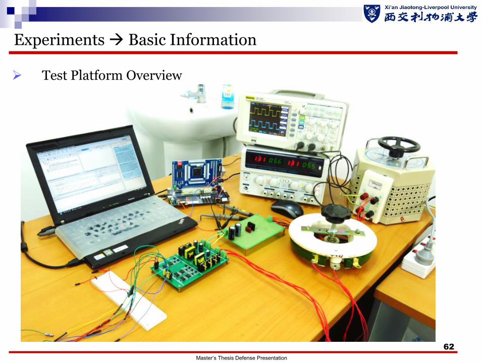
Test Platform Overview
Experiments Basic Information
Master’s Thesis Defense Presentation
63
Experiments Basic Information
DAB-BDC
DSP
LOAD
AC/DC
AC Power
Master’s Thesis Defense Presentation
64
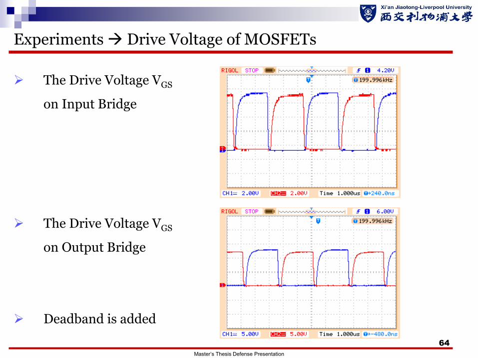
Experiments Drive Voltage of MOSFETs
Master’s Thesis Defense Presentation
The Drive Voltage VGS
on Input Bridge
The Drive Voltage VGS
on Output Bridge
Deadband is added
65
Experiments The Transformer Voltage (Primary Side)
Master’s Thesis Defense Presentation
Verified the Theoretical Analysis
66
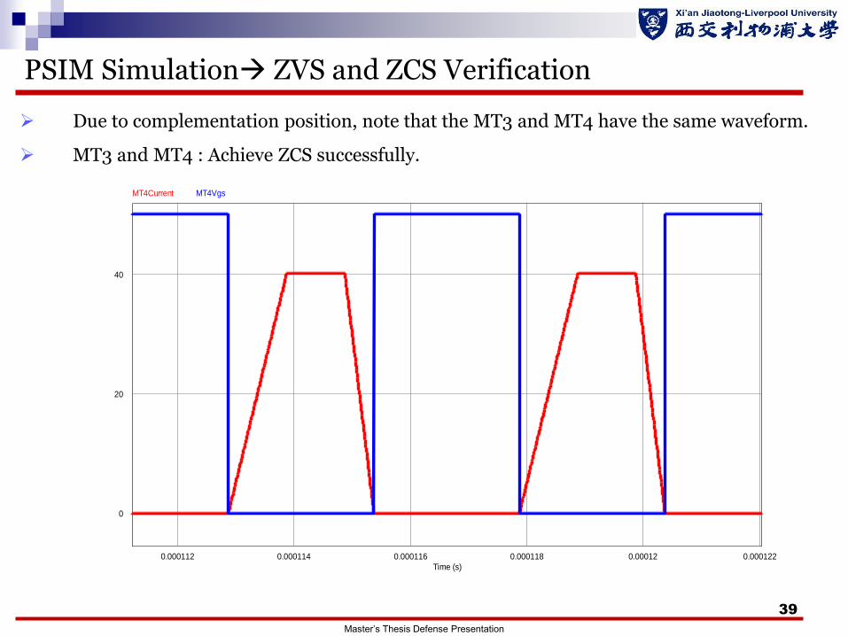
Experiments Soft Switching Condition Verification
The VGS and VDS on
Input Bridge
The VGS and VDS on
Output Bridge
Master’s Thesis Defense Presentation
67
Experiments Limitations
The laboratory does not have High Voltage DC Power
Supply.
The 60V DC Power Supply : Output with Huge Ripple
Can not provide a 300 W , 200V input, thus no results to
evaluate the efficiency.
Now : 60V, 50W, Light Load, Verified the basic function.
Master’s Thesis Defense Presentation
68
Conclusions
Summary
Future Work
Chapter 6
Master’s Thesis Defense Presentation
69
1. Renewable energy systems needs energy storage unit and DAB-BDC
transfers the energy in bidirectional way.
2. Discussed a improved topology of bidirectional DAB DC/DC converter
that can eliminate the circulation energy losses (Compare traditional
DAB).
3. Fully theoretical analysis was done.
4. Based on PSIM software, simulation was done.
5. A 300W prototype was built and experiment results verified the
previous analysis.
Conclusions Summary
Master’s Thesis Defense Presentation
70
1. Get High Quality DC power supply and evaluate the efficiency.
2. Open loop and not sufficiently stable Small signal model and PI
controller improve the stable ability.
3. Full order continuous time average model for DC/DC DAB converters
will be developed.
4. Try to adapt the DAB BDC into the renewable energy systems such as PV
array generation, wind turbine or tidal power generation.
Conclusions Future Work
Master’s Thesis Defense Presentation
71
Reference (Part)
Master’s Thesis Defense Presentation
1. Maureen Lorenzetti, “BP: World oil and gas reserves still growing at healthy pace” Oil and gas journal, June 2004.
2. Xiaodong Li; Bhat, A. K S, "Analysis and Design of High-Frequency Isolated Dual-Bridge Series Resonant DC/DC Converter," Power Electronics,
IEEE Transactions on , vol.25, no.4, pp.850,862, April 2010.
3. H. J. Chiu and L. W. Lin, "A bidirectional dc-dc converter for fuel cell electric vehicle driving system," IEEE Trans. Power Electron., vol. 21, no. 4,
pp. 950-958, July 2006.
4. S. Jalbrzykowski, A. Bogdan and Tadeusz Citko, "A dual full-bridge resonant class-e bidirectional dc-dc converter," IEEE Trans. Industrial
Electron., vol. 58, no. 9, pp. 3879-3883, September 2011.
5. L. Sh. Yang and T. J. Liang, "Analysis and implementation of a novel bidirectional dc-dc converter," IEEE Trans. Industrial Electron., vol. 59, no.
1,p.p 422-434, January 2012.
6. Zhu, L., "A Novel Soft-Commutating Isolated Boost Full-Bridge ZVS-PWM DC–DC Converter for Bidirectional High Power Applications," Power
Electronics, IEEE Transactions on , vol.21, no.2, pp.422,429, March 2006.
7. N. M. L. Tan, T. Abe and H. Akagi, "Topology and Application of Bidirectional Isolated DC-DC Converters," 8th International Conference on Power
Electronics - ECCE Asia, p-p1039-1046, June 2011.
8. Huang-Jen Chiu; Li-Wei Lin, "A bidirectional DC-DC converter for fuel cell electric vehicle driving system," Power Electronics, IEEE Transactions
on, vol.21, no.4, pp.950,958, July 2006.
9. Zhe Zhang; Thomsen, O.C.; Andersen, M. A E; Nielsen, H.R., "A novel dual-input isolated current-fed DC-DC converter for renewable energy
system," Applied Power Electronics Conference and Exposition (APEC), 2011 Twenty-Sixth Annual IEEE , vol., no., pp.1494,1501, 6-11 March
2011.
10. Babokany, A.S.; Jabbari, M.; Shahgholian, G.; Mahdavian, Mehdi, "A review of bidirectional dual active bridge converter," Electrical
Engineering/Electronics, Computer, Telecommunications and Information Technology (ECTI-CON), 2012 9th International Conference on , vol.,
no., pp.1,4, 16-18 May 2012.
11. Jung-Goo Cho; Sabate, J.A.; Hua, G.; Lee, F.C., "Zero-voltage and zero-current-switching full bridge PWM converter for high-power
applications," Power Electronics, IEEE Transactions on , vol.11, no.4, pp.622,628, Jul 1996.
12. R. De Doncker, D. Divan, and M. Kheraluwala, “A three-phase soft-switched high-power-density dc/dc converter for high-power applications,” IEEE
Transactions on Industry Application, vol. 27, pp. 63–73, Jan./Feb. 1991.
13. M. N. Kheraluwala, R. W. Gascoigne, D. M. Divan, and E. D. Baumann, “Performance characterization of a high-power dual active bridge,” IEEE
Transactions on Industry Application, vol. 28, pp. 1294–1301, Jun. 1992.
14. Kunrong Wang; Lee, F.C.; Lai, J., "Operation principles of bi-directional full-bridge DC/DC converter with unified soft-switching scheme and soft-
starting capability," Applied Power Electronics Conference and Exposition, 2000. APEC 2000. Fifteenth Annual IEEE, vol.1, no., pp.111,118 vol.1,
2000.
15. Kheraluwala, M.N.; Gascoigne, R.W.; Divan, D.M.; Baumann, E.D., "Performance characterization of a high-power dual active bridge DC-to-DC
converter," Industry Applications, IEEE Transactions on , vol.28, no.6, pp.1294,1301, Nov/Dec 1992.
16. Zhang, J.M.; Xu, D.M.; Zhaoming Qian, "An improved dual active bridge DC/DC converter," Power Electronics Specialists Conference, 2001.