ISSN: 2237-0722 Vol. 11 No. 4 (2021) Received: 13.06.2021 – Accepted: 15.07.2021 3336 Bidirectional DC-DC Converter Using Zero Voltage Switching Y. Sukhi 1 ; Y. Jeyashree 2 ; A. Jenifer 3 ; S. Anita 4 ; A. Fayaz Ahamed 5 1 EEE Department, SRMIST, Kattankulathur, Tamil Nadu, India. 2 EEE Department, R.M.K. Engineering College, Kavaraipettai, Tamil Nadu, India. 3 EEE Department, SRMIST, Kattankulathur, Tamil Nadu, India. 4 EEE Department, SRMIST, Kattankulathur, Tamil Nadu, India. 5 EEE Department, SRMIST, Kattankulathur, Tamil Nadu, India. Abstract DC-DC Converters are used for storage of energy from renewable energy resources. These converters uses zero voltage switching concept to reduce the losses. In order to increase the operating range of the converter duty ratio is varied using effective control technique. By changing the duty ratio with transformer in the output, zero switching losses can be obtained over the full range of duty cycle by the voltage second balancing. Analysis of two port and three port converters is done and simulated to verify the analysis. Key-words: DC-DC Converter, Renewable Energy Resources, Zero Voltage Switching. 1. Introduction A chopper is used in a circuit when the load is connected to the source certain interval of time to the load and is disconnected from the load during the remining time interval. This is repeated to get the desired output. The speed of operation of thyristor switch is high. To make the switch in on mode it needs gate signal. It can be turned off by forced commutation method. Chopper is used to convert the level of output voltage to a required variable voltage or constant voltage. Therefore it is named as dc-dc converter. The chopper circuit can be used to increase the output voltage or decrease the output voltage. The thyristors are unidirectional due to the flow of current is only in one direction, because the thyristor allows the current in only one direction. DC-DC converters are operated in soft switching mode of operation. These converters are unidirectional and its rating is less. But the bidirectional converters are more suitable for battery charging. The soft switching technique is
Transcript
ISSN: 2237-0722
Vol. 11 No. 4 (2021)
Received: 13.06.2021 – Accepted: 15.07.2021
3336
Bidirectional DC-DC Converter Using Zero Voltage Switching
Y. Sukhi1; Y. Jeyashree2; A. Jenifer3; S. Anita4; A. Fayaz Ahamed5
1EEE Department, SRMIST, Kattankulathur, Tamil Nadu, India. 2EEE Department, R.M.K. Engineering College, Kavaraipettai, Tamil Nadu, India.
3EEE Department, SRMIST, Kattankulathur, Tamil Nadu, India. 4EEE Department, SRMIST, Kattankulathur, Tamil Nadu, India. 5EEE Department, SRMIST, Kattankulathur, Tamil Nadu, India.
Abstract
DC-DC Converters are used for storage of energy from renewable energy resources. These
converters uses zero voltage switching concept to reduce the losses. In order to increase the
operating range of the converter duty ratio is varied using effective control technique. By changing
the duty ratio with transformer in the output, zero switching losses can be obtained over the full
range of duty cycle by the voltage second balancing. Analysis of two port and three port converters is
done and simulated to verify the analysis.
Key-words: DC-DC Converter, Renewable Energy Resources, Zero Voltage Switching.
1. Introduction
A chopper is used in a circuit when the load is connected to the source certain interval of time
to the load and is disconnected from the load during the remining time interval. This is repeated to get
the desired output. The speed of operation of thyristor switch is high. To make the switch in on mode
it needs gate signal. It can be turned off by forced commutation method. Chopper is used to convert
the level of output voltage to a required variable voltage or constant voltage. Therefore it is named as
dc-dc converter. The chopper circuit can be used to increase the output voltage or decrease the output
voltage. The thyristors are unidirectional due to the flow of current is only in one direction, because
the thyristor allows the current in only one direction. DC-DC converters are operated in soft
switching mode of operation. These converters are unidirectional and its rating is less. But the
bidirectional converters are more suitable for battery charging. The soft switching technique is
ISSN: 2237-0722
Vol. 11 No. 4 (2021)
Received: 13.06.2021 – Accepted: 15.07.2021
3337
employed in full bridge converter. There is high ripple content in voltage source converter. The clamp
circuit is required for a current source converter. This type of bidirectional converters uses less
number of components because same components are used for both the direction. Also the proposed
converter circuit for the battery charging has less ripple content. The stress on the switches is less.
The loss component of the converter is less due to minimum number of components. The converter
is subjected to fast changeover during fault condition and also the reappearance is quick. This is
widely in charging of batteries, uninterruptable power supply units, computer power supply units, and
also in telecommunication units. In case of buck converter the output voltage is lesser than the input
voltage. Electronic power supplies are operated using this principle. The input ac voltage is
converted to low level dc voltage using rectifier for the power supply unit. This rectified dc voltage is
changed low level dc output voltage. The second stage is a current source. During reverse operation
also, the output voltage is lesser than the input voltage. This is acting as a boost converter. The buck
and boost operation are functioning parallel. The parameters are fixed and the values of the
parameters are maintained by the switching action. Due to assumption of ideal elements used in the
circuit, the input power is taken as equal to the output power. There is no energy loss the circuit
elements of the converter. The output voltage and the input currents have ripples. In case of a
conventional buck converter the current direction is always from the source to the load and the input
voltage is higher than the output voltage. The ripple occurs in both input current and output voltage.
In a conventional buck converter, there is one direction for current flow and the input voltage is
always higher than output voltage. This reduces the number of switching elements used in the
converter topology. When there are two switches, these switches are operating alternatively. When
one switch is in on condition, the other is operating in blocking mode and does not allow the current.
The second device need not be in a switching device. It can also be a diode. The implementation
using diode increases the conduction losses. Series inductor is used in the circuit to develop the
effect of constant current. The input inductor in the input side of the boost converter develops the
constant current. The interfacing device, capacitor, gives rise to voltage source at the output. The
basic functions for dc-dc converter are Vout <Vin for the buck and Vout > Vin for the boost. This is
similar to the transformer function. In the cascade connection, indirect converter is obtained from two
direct converter connection. In this cacade connection, adjustments of each converter is done
independently to get the required output voltage. A bidirectional dc-dc converter is used in which the
power can flow from dc source to battery while charging and from battery while discharging. This
bidirectional operation of the converter can be obtained using the rectifier, transformer and inverter.
The transformer used in the converter provides isolation between high voltage side and low voltage
ISSN: 2237-0722
Vol. 11 No. 4 (2021)
Received: 13.06.2021 – Accepted: 15.07.2021
3338
side with unity turns ratio. The source side is high voltage side and output is the low voltage side.
The primary side of the converter is a half bridge and is connected to the dc mains. The secondary
side, connected to the battery, forms a current-fed push-pull. The shows a balancing winding Np1 and
two catching diodes D1 and D2 on the primary side of the half bridge. They maintain the center point
voltage at the junction of C1 and C2 to one half of the input voltage. Here Np1 and Np2 windings
have the same number of windings. Bidirectional converters can be implemented using the topologies
such as resonant, soft switching and hard switching PWM. But these topologies have the following
disadvantages are Increase in component ratings, Circuit complexity, Conduction losses, High output
current ripple, Older methods uses rectifier diode network to reduce the voltage. This network looks
simple but suffers from power losses. Thus the effort to complete DC to DC conversion without the
use of resistor in the conversion circuit. Hence a circuit is more efficient when compared with others.
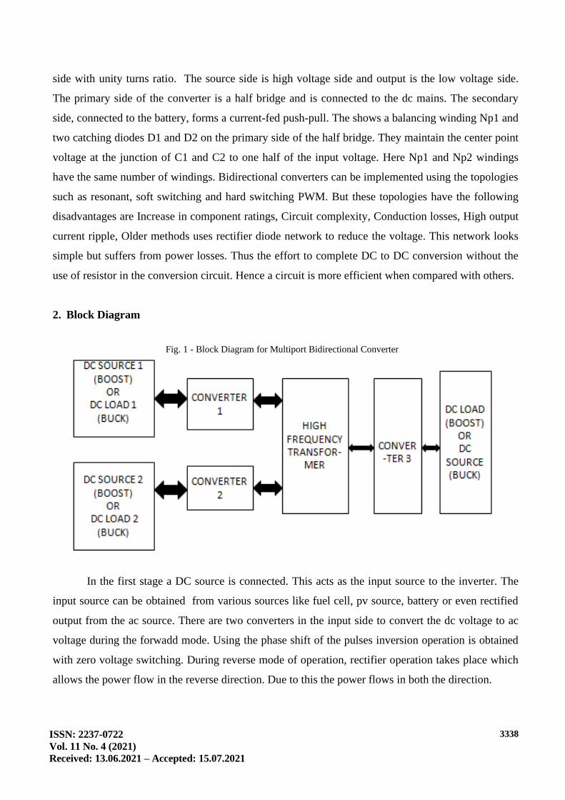
2. Block Diagram
Fig. 1 - Block Diagram for Multiport Bidirectional Converter
In the first stage a DC source is connected. This acts as the input source to the inverter. The
input source can be obtained from various sources like fuel cell, pv source, battery or even rectified
output from the ac source. There are two converters in the input side to convert the dc voltage to ac
voltage during the forwadd mode. Using the phase shift of the pulses inversion operation is obtained
with zero voltage switching. During reverse mode of operation, rectifier operation takes place which
allows the power flow in the reverse direction. Due to this the power flows in both the direction.
ISSN: 2237-0722
Vol. 11 No. 4 (2021)
Received: 13.06.2021 – Accepted: 15.07.2021
3339
The step down voltage is done and it is applied to the load through high frequency
transformer. Since the frequency is high the size of the transformer is small. In this the converter 3 is
used for the conversion of dc output voltage to ac voltage. This is the inverse operation. The same
converter 3 acts as rectifier during forward conduction mode. In this forward conduction mode ac
voltage is convertered to do voltage. This voltage is applied to the load.This converter can be used for
battery charging, telecom and also in drives.
3. Multi-Port Converter
Multiport converters are widely used in renewable energy applications. The research is
increasing in this field. The cost involved for this converter is less because more number of outputs
can be taken from single converter. Due to single stage in the converter power conversion efficiency
of these multi port converters are good. The dual active bridge converter is used for dc-dc power
conversion. This converter has some attractive features like less stress, constant frequency of
operation, power flow in both direction, leakage inductance in the transformer is used as energy
transfer element. The voltage stress across the switches is less due to soft switching in the on/off
condition. The constant frequency operation is simple to process. The number of devices is reduced
due to the bidirectional power flow. But this type of configuration cannot be implemented when the
voltage range is wide which occur in pv application, fuel cell. This will reduce the soft switching
frequency ranges. As a development of dual active bridge converter, triple active bridge converter for
three port system is developed. This can be developed for the applications like battery charging. The
zero voltage switching cannot be applied to dual active bridge converter and triple active bridge
converter for low voltage ranges. By including an inductor in parallel with the transformer
connection, the zero voltage switching can be applied for all range of inputs. Voltage cancellation is
proposed to increase the duty ratio. The phase shift of pulse can also be applied for the extension of
zero voltage switching. The technique utilizes a disconnected determined query table of the control
points with the yield current and voltage (V-I plane) as the look-into boundaries. The objective is to
control the defer point of the terminating sign of one of the scaffold legs, and thusly the zero-
intersection of the current, with the end goal that every one of the switches are delicate exchanged. In
any case, the depicted strategy is intricate to carry out and conditions for computing the points have
not been distributed. Obligation proportion control was likewise utilized for changing the abundancy
of the crucial part, however not unequivocally for expanding the ZVS range. Furthermore, a stage
shift in addition to beat width-adjustment (PWM) control was applied to the DAB converter, where
ISSN: 2237-0722
Vol. 11 No. 4 (2021)
Received: 13.06.2021 – Accepted: 15.07.2021
3340
the converter utilizes two half-extensions to create topsy-turvy waveforms to manage the voltage
variety. Be that as it may, for the multiport geographies, with this strategy just one port may have a
wide working voltage since every one of the extensions work at a similar obligation proportion.
Utilizing a - comparable model of the transformer organization to investigate the force stream in a
three-port framework has been examined. This methodology improves on the examination of the
force stream. For the TAB converter obligation proportion control can be utilized to make up for
voltage varieties at the ports. We recommend that the obligation proportion is forced by the working
voltage of the port, being conversely relative. In multiport geographies it is thusly conceivable to
stretch out the ZVS working reach to the whole working area. The manner by which the obligation
proportion is controlled is basically different. The strategy utilizes a disconnected determined query
table of the control points with the yield current and voltage (V-I plane) as the look-into boundaries.
The objective is to control the postpone point of the terminating sign of one of the extension legs, and
along these lines the zero-intersection of the current, to such an extent that every one of the switches
are delicate exchanged. Nonetheless, the depicted strategy is unpredictable to carry out and conditions
for computing the points have not been distributed. Obligation proportion control was additionally
utilized for changing the sufficiency of the crucial segment, yet not unequivocally for expanding the
ZVS range. Moreover, a stage shift in addition to beat width-tweak (PWM) control was applied to the
DAB converter, where the converter utilizes two half-extensions to create awry waveforms to manage
the voltage variety. Be that as it may, for the multiport geographies, with this technique just one port
may have a wide working voltage since every one of the scaffolds work at a similar obligation
proportion. Utilizing a - identical model of the transformer organization to break down the force
stream in a three-port framework has been examined. This methodology works on the examination of
the force stream. For the TAB converter obligation proportion control can be utilized to make up for
voltage varieties at the ports. We recommend that the obligation proportion is forced by the working
voltage of the port, being contrarily relative. In multiport geographies it is thusly conceivable to
stretch out the ZVS working reach to the whole working locale. The manner by which the obligation
proportion is controlled is basically extraordinary.
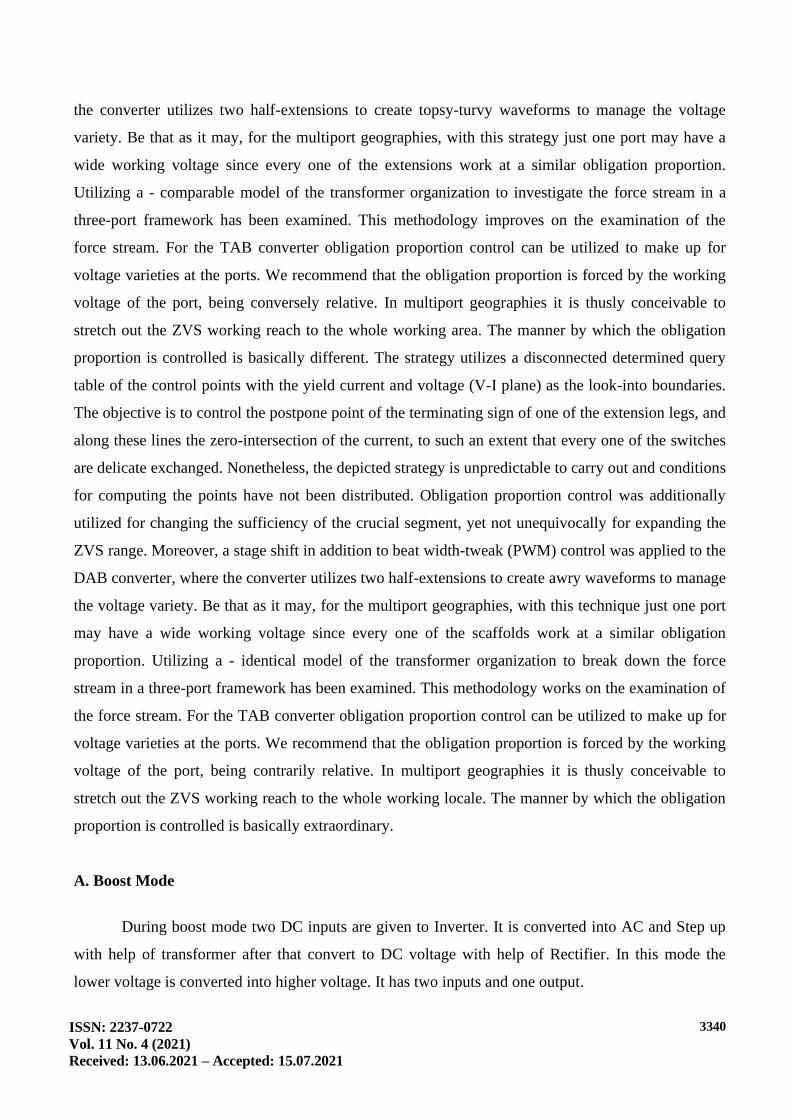
A. Boost Mode
During boost mode two DC inputs are given to Inverter. It is converted into AC and Step up
with help of transformer after that convert to DC voltage with help of Rectifier. In this mode the
lower voltage is converted into higher voltage. It has two inputs and one output.
ISSN: 2237-0722
Vol. 11 No. 4 (2021)
Received: 13.06.2021 – Accepted: 15.07.2021
3341
Fig. 2 - Circuit Diagram for Boost Mode
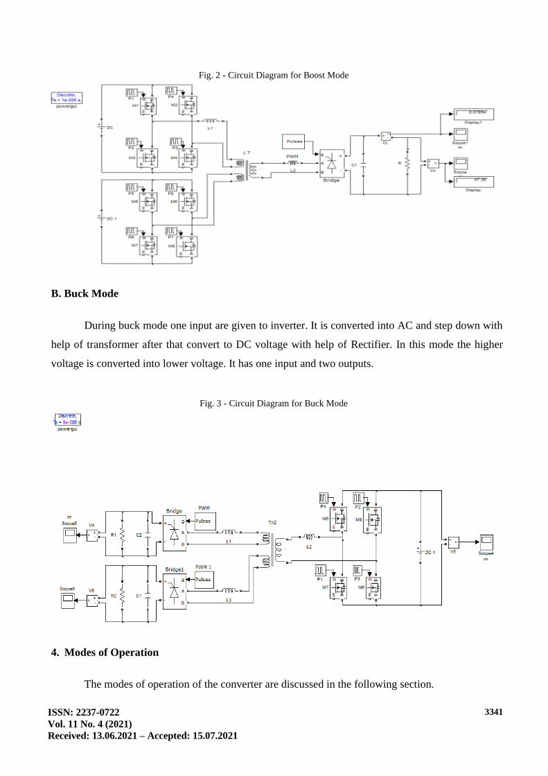
B. Buck Mode
During buck mode one input are given to inverter. It is converted into AC and step down with
help of transformer after that convert to DC voltage with help of Rectifier. In this mode the higher
voltage is converted into lower voltage. It has one input and two outputs.
Fig. 3 - Circuit Diagram for Buck Mode
4. Modes of Operation
The modes of operation of the converter are discussed in the following section.
ISSN: 2237-0722
Vol. 11 No. 4 (2021)
Received: 13.06.2021 – Accepted: 15.07.2021
3342
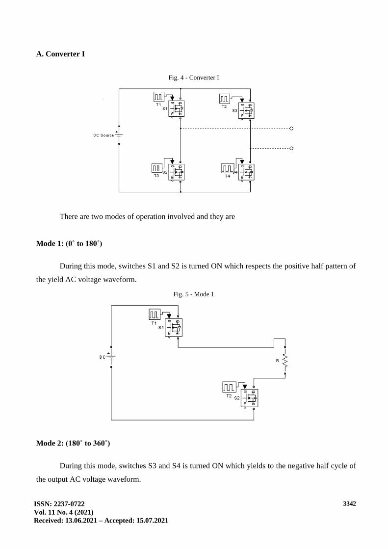
A. Converter I
Fig. 4 - Converter I
There are two modes of operation involved and they are
Mode 1: (0˚ to 180˚)
During this mode, switches S1 and S2 is turned ON which respects the positive half pattern of
the yield AC voltage waveform.
Fig. 5 - Mode 1
Mode 2: (180˚ to 360˚)
During this mode, switches S3 and S4 is turned ON which yields to the negative half cycle of
the output AC voltage waveform.
ISSN: 2237-0722
Vol. 11 No. 4 (2021)
Received: 13.06.2021 – Accepted: 15.07.2021
3343
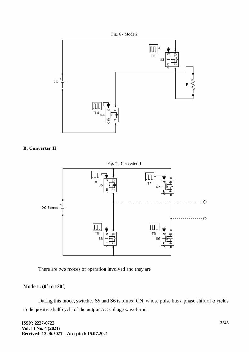
Fig. 6 - Mode 2
B. Converter II
Fig. 7 - Converter II
There are two modes of operation involved and they are
Mode 1: (0˚ to 180˚)
During this mode, switches S5 and S6 is turned ON, whose pulse has a phase shift of α yields
to the positive half cycle of the output AC voltage waveform.
ISSN: 2237-0722
Vol. 11 No. 4 (2021)
Received: 13.06.2021 – Accepted: 15.07.2021
3344
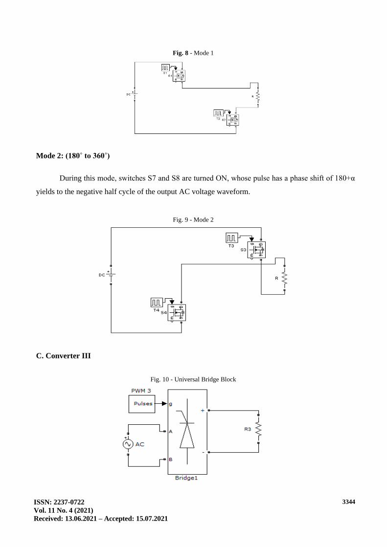
Fig. 8 - Mode 1
Mode 2: (180˚ to 360˚)
During this mode, switches S7 and S8 are turned ON, whose pulse has a phase shift of 180+α
yields to the negative half cycle of the output AC voltage waveform.
Fig. 9 - Mode 2
C. Converter III
Fig. 10 - Universal Bridge Block
ISSN: 2237-0722
Vol. 11 No. 4 (2021)
Received: 13.06.2021 – Accepted: 15.07.2021
3345
Set number of extension arms to 1 or 2 to get a solitary stage converter (two or four
exchanging gadgets). Set to 3 to get a three-stage converter associated in Graetz connect design (six
exchanging gadgets). The snubber opposition, in ohms (Ω). Set the Snubber obstruction Rs boundary
to inf to kill the snubbers from the model. The snubber capacitance, in farads (F). Set the Snubber
capacitance Cs boundary to 0 to dispense with the snubbers, or to inf to get a resistive snubber. To
keep away from mathematical motions when your framework is discretized, you need to indicate Rs
and Cs snubber qualities for diode and thyristor spans. For constrained commutated gadgets (GTO,
IGBT, or MOSFET), the scaffold works agreeably with absolutely resistive snubbers insofar as
terminating beats are shipped off exchanging gadgets. In the event that terminating heartbeats to
constrained commutated gadgets are obstructed, just antiparallel diodes work, and the scaffold works
as a diode rectifier. In this condition proper upsides of Rs and Cs should likewise be utilized.
Fig. 11 - Switching Waveform for Universal Bridge
The advantages are handling large power, Power flow in both directions, Less switching
losses due to ZVS, Improve the efficiency, Transformer size is small and the applications are Power
supply for DC motor, Battery charging, Battery operated Electric vehicle, Traction Purpose.
5. Simulation and Results
Simulation has become an incredible asset on the business application just as in scholastics,
these days. It is presently fundamental for an electrical architect to comprehend the idea of
reenactment and gain proficiency with its utilization in different applications. Reproduction is
perhaps the most ideal approaches to examine the framework or circuit conduct without harming it.
The instruments for doing the recreation in different fields are accessible on the lookout for designing
experts. Numerous businesses are investing a lot of energy and cash in doing recreation prior to
assembling their item. In a large portion of the innovative work, the renovation assumes a vital part.
ISSN: 2237-0722
Vol. 11 No. 4 (2021)
Received: 13.06.2021 – Accepted: 15.07.2021
3346
Without recreation it hushes up difficult to continue further. It ought to be noticed that in power
gadgets, PC reproduction and a proof of idea equipment model in the research facility are free to one
another. Anyway PC reenactment should not be considered as a substitute for equipment model. The
goal of this part is to portray reenactment of impedance source inverter with R, R-L and RLE loads
utilizing MATLAB instrument.
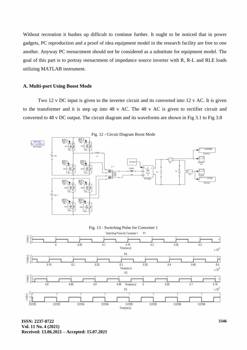
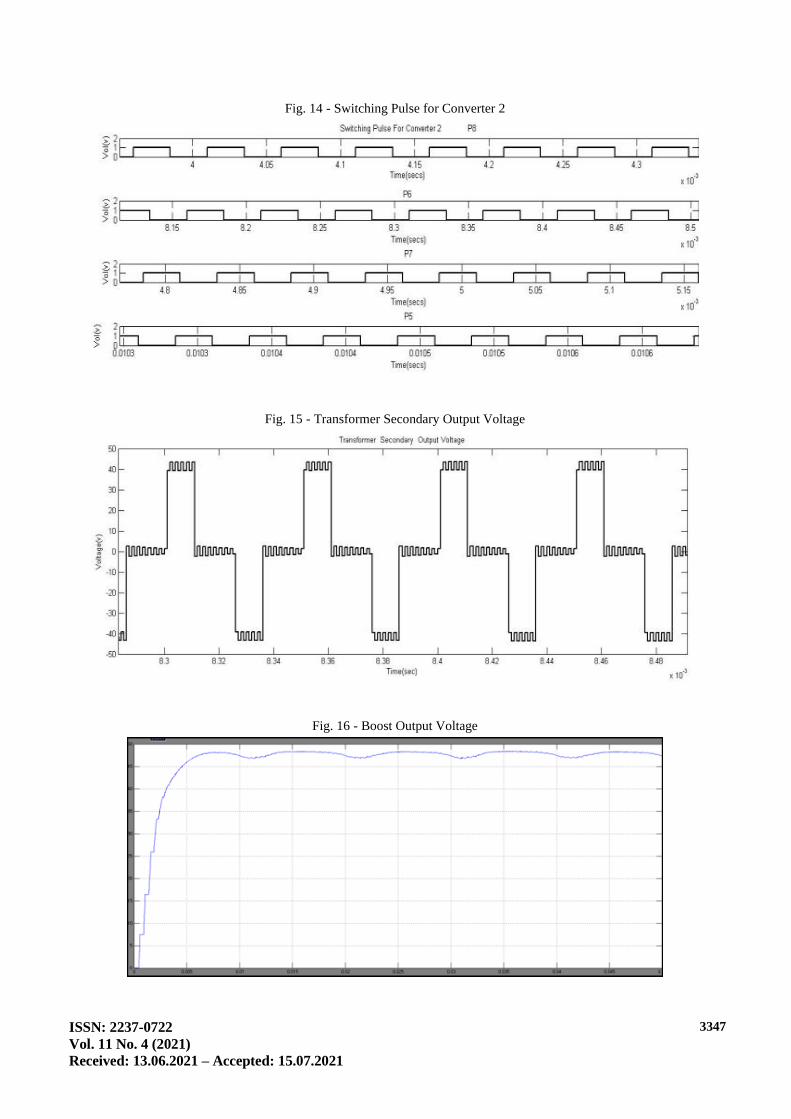
A. Multi-port Using Boost Mode
Two 12 v DC input is given to the inverter circuit and its converted into 12 v AC. It is given
to the transformer and it is step up into 48 v AC. The 48 v AC is given to rectifier circuit and
converted to 48 v DC output. The circuit diagram and its waveforms are shown in Fig 3.1 to Fig 3.8
Fig. 12 - Circuit Diagram Boost Mode
Fig. 13 - Switching Pulse for Converter 1
ISSN: 2237-0722
Vol. 11 No. 4 (2021)
Received: 13.06.2021 – Accepted: 15.07.2021
3347
Fig. 14 - Switching Pulse for Converter 2
Fig. 15 - Transformer Secondary Output Voltage
Fig. 16 - Boost Output Voltage
ISSN: 2237-0722
Vol. 11 No. 4 (2021)
Received: 13.06.2021 – Accepted: 15.07.2021
3348
Fig. 17 - Boost Output Current
Fig. 18 - Boost Input Voltage 1
Fig. 19 - Boost Input Voltage 2
B. Multi-port Using Buck Mode
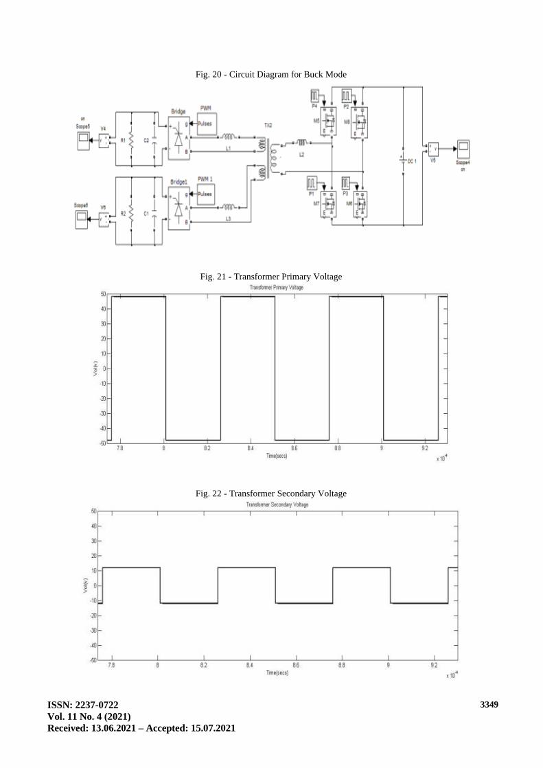
A 48v DC input is given to the inverter circuit and it’s converted to 48 v AC. This 48 v AC is
given to the transformer and its step down to 12 v AC. This 12 v AC is given to the rectifier circuit
and it is converted into two 12 v DC output. The circuit diagram and its waveform are shown in Fig.
ISSN: 2237-0722
Vol. 11 No. 4 (2021)
Received: 13.06.2021 – Accepted: 15.07.2021
3349
Fig. 20 - Circuit Diagram for Buck Mode
Fig. 21 - Transformer Primary Voltage
Fig. 22 - Transformer Secondary Voltage
ISSN: 2237-0722
Vol. 11 No. 4 (2021)
Received: 13.06.2021 – Accepted: 15.07.2021
3350
Fig. 23 - Buck Output Voltage 1
Fig. 24 - Buck Output Voltage 2
Fig. 25 - Buck Input Voltage
ISSN: 2237-0722
Vol. 11 No. 4 (2021)
Received: 13.06.2021 – Accepted: 15.07.2021
3351
6. Conclusion
This paper explains the performance and operation of triple port bi-directional DC-DC
converter. Another delicate exchanged segregated bidirectional dc–dc converter has been introduced
in this paper. The activity, examination, highlights and plan thought were delineated. Recreation
result s were displayed to check the activity standard. It is shown that ZVS one or the other way of
force stream is accomplished with no lossy segments included and no extra dynamic switch. This
gives the double capacities (synchronous lift change and reversal) given by the low voltage side half
scaffold, current weights on the exchanging gadgets and transformer are kept least. It is shown that
the base generally framework misfortunes, regardless of the port voltage has a fixed worth or a wide
reach, is feasible by ZVS control. In this an isolated three port bi-directional topology, which consist
of three converter units and a high frequency three winding transformer is analyzed by simulation.
References
J. Marcos Alonso, Antonio J. Calleja, Javier Ribas, Emilio López Corominas,Manuel Rico-Secades,
Analysis and Design of a Novel Single-Stage High-Power-Factor Electronic Ballast based on
Integrated Buck Half-Bridge Resonant Inverter, IEEE Transactions on Power Electronics, 19(2),


![BIDIRECTIONAL DC-to-DC CONVERTER WITH · PDF fileBIDIRECTIONAL DC-to-DC CONVERTER WITH EXTENDED VOLTAGE TRANSFER RATIO ... well-known push-pull converter [3] ... IRF840 (S3 &](https://static.documents.pub/doc/80x56/5abe38867f8b9a3a428cb169/bidirectional-dc-to-dc-converter-with-dc-to-dc-converter-with-extended-voltage.jpg)


