Cation-based resistive memory Emerging Non-Volatile Memory Technologies Symposium San Francisco Bay Area Nanotechnology Council April 6, 2012 Michael N. Kozicki Professor of Electrical Engineering School of Electrical, Computer, and Energy Engineering, ASU Chief Scientist, Adesto Technologies Corp.
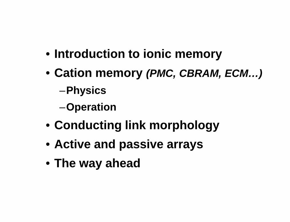
• Conducting link morphology • Active and passive arrays • The way ahead
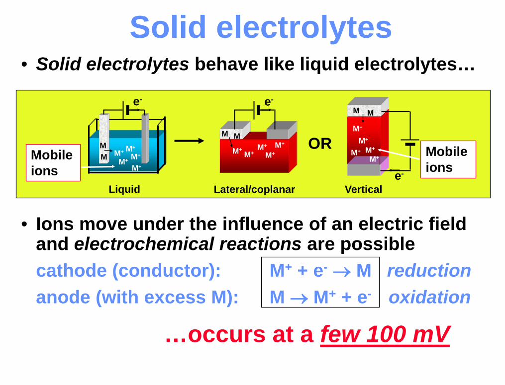
Solid electrolytes • Solid electrolytes behave like liquid electrolytes…
• Ions move under the influence of an electric field and electrochemical reactions are possible
cathode (conductor): M+ + e- → M reduction anode (with excess M): M → M+ + e- oxidation
…occurs at a few 100 mV
OR M+
M+
M+
M+
M+
M+ M+ M+
M+ M+
M+
M+
M+
M+ M+
e- e-
e-
Mobile ions
Mobile ions
Liquid Lateral/coplanar Vertical
M
M
M M
M M
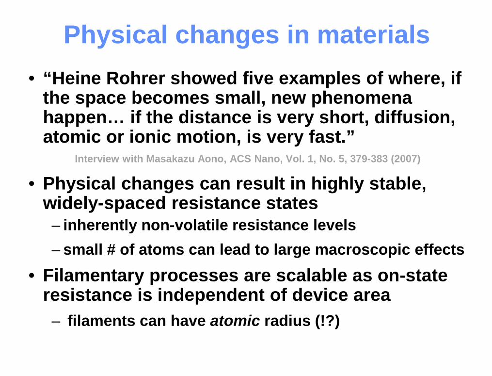
• “Heine Rohrer showed five examples of where, if the space becomes small, new phenomena happen… if the distance is very short, diffusion, atomic or ionic motion, is very fast.”
• Physical changes can result in highly stable, widely-spaced resistance states
– inherently non-volatile resistance levels – small # of atoms can lead to large macroscopic effects
• Filamentary processes are scalable as on-state resistance is independent of device area
– filaments can have atomic radius (!?)
Physical changes in materials
…ion-migration effects are coupled to redox processes which cause the change in resistance. They are subdivided into cation-migration cells, based on the electrochemical growth and dissolution of metallic filaments, and anion-migration cells, typically realized with transition metal oxides as the insulator, in which electronically conducting paths of sub-oxides are formed and removed…
nature materials | VOL 6 | NOVEMBER 2007 | www.nature.com/naturematerials
• Conducting link morphology • Active and passive arrays • The way ahead
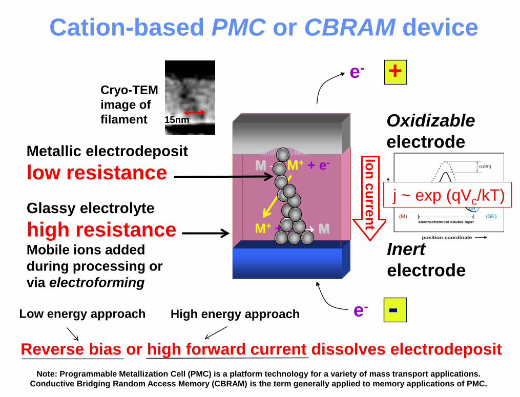
Glassy electrolyte high resistance Mobile ions added during processing or via electroforming
Inert electrode
Oxidizable electrode
+
-
M → M+ + e-
M+ + e- → M
e-
e-
Reverse bias or high forward current dissolves electrodeposit
Ion current
Low energy approach High energy approach
Metallic electrodeposit low resistance
Cation-based PMC or CBRAM device
Cryo-TEM image of filament 15nm
Note: Programmable Metallization Cell (PMC) is a platform technology for a variety of mass transport applications. Conductive Bridging Random Access Memory (CBRAM) is the term generally applied to memory applications of PMC.
azeE Wa0
Applied Field E j ~ exp (qVc/kT)
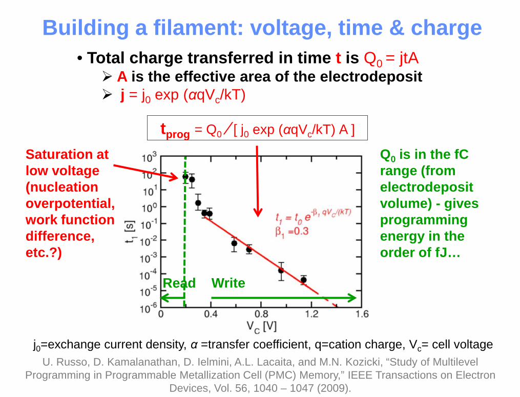
Building a filament: voltage, time & charge
Saturation at low voltage (nucleation overpotential, work function difference, etc.?)
• Total charge transferred in time t is Q0 = jtA A is the effective area of the electrodeposit j = j0 exp (αqVc/kT)
tprog = Q0 ⁄ [ j0 exp (αqVc/kT) A ]
j0=exchange current density, α =transfer coefficient, q=cation charge, Vc= cell voltage U. Russo, D. Kamalanathan, D. Ielmini, A.L. Lacaita, and M.N. Kozicki, “Study of Multilevel
Programming in Programmable Metallization Cell (PMC) Memory,” IEEE Transactions on Electron Devices, Vol. 56, 1040 – 1047 (2009).
Q0 is in the fC range (from electrodeposit volume) - gives programming energy in the order of fJ…
Write Read
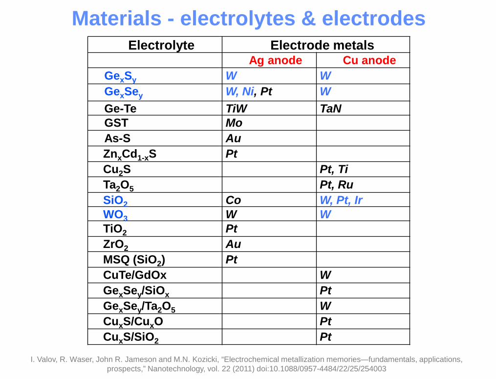
Electrolyte Electrode metals Ag anode Cu anode
GexSy W W GexSey W, Ni, Pt W Ge-Te TiW TaN GST Mo As-S Au ZnxCd1-xS Pt Cu2S Pt, Ti Ta2O5 Pt, Ru SiO2 Co W, Pt, Ir WO3 W W TiO2 Pt ZrO2 Au MSQ (SiO2) Pt CuTe/GdOx W GexSey/SiOx Pt GexSey/Ta2O5 W CuxS/CuxO Pt CuxS/SiO2 Pt
Materials - electrolytes & electrodes
I. Valov, R. Waser, John R. Jameson and M.N. Kozicki, “Electrochemical metallization memories—fundamentals, applications, prospects,” Nanotechnology, vol. 22 (2011) doi:10.1088/0957-4484/22/25/254003
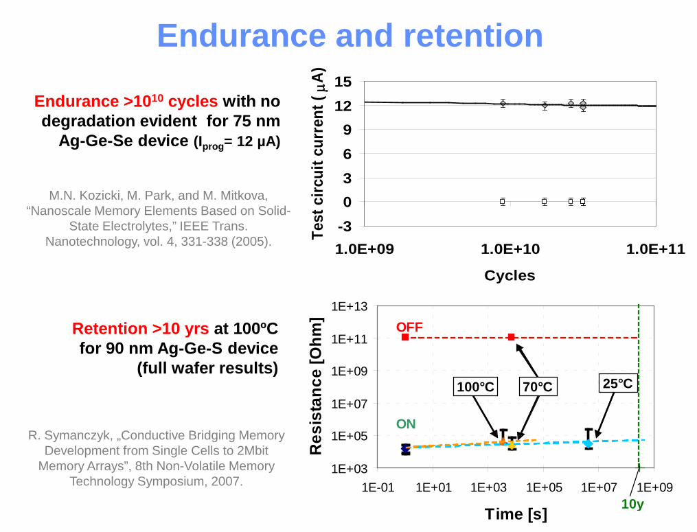
M.N. Kozicki, M. Park, and M. Mitkova, “Nanoscale Memory Elements Based on Solid-
State Electrolytes,” IEEE Trans. Nanotechnology, vol. 4, 331-338 (2005).
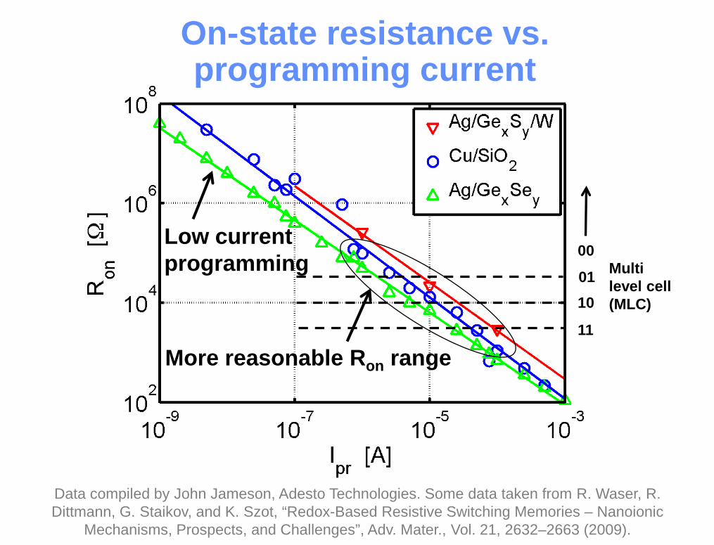
On-state resistance vs. programming current
Low current programming
More reasonable Ron range
Data compiled by John Jameson, Adesto Technologies. Some data taken from R. Waser, R. Dittmann, G. Staikov, and K. Szot, “Redox-Based Resistive Switching Memories – Nanoionic
Mechanisms, Prospects, and Challenges”, Adv. Mater., Vol. 21, 2632–2663 (2009).
00
01 10
11
Multi level cell (MLC)
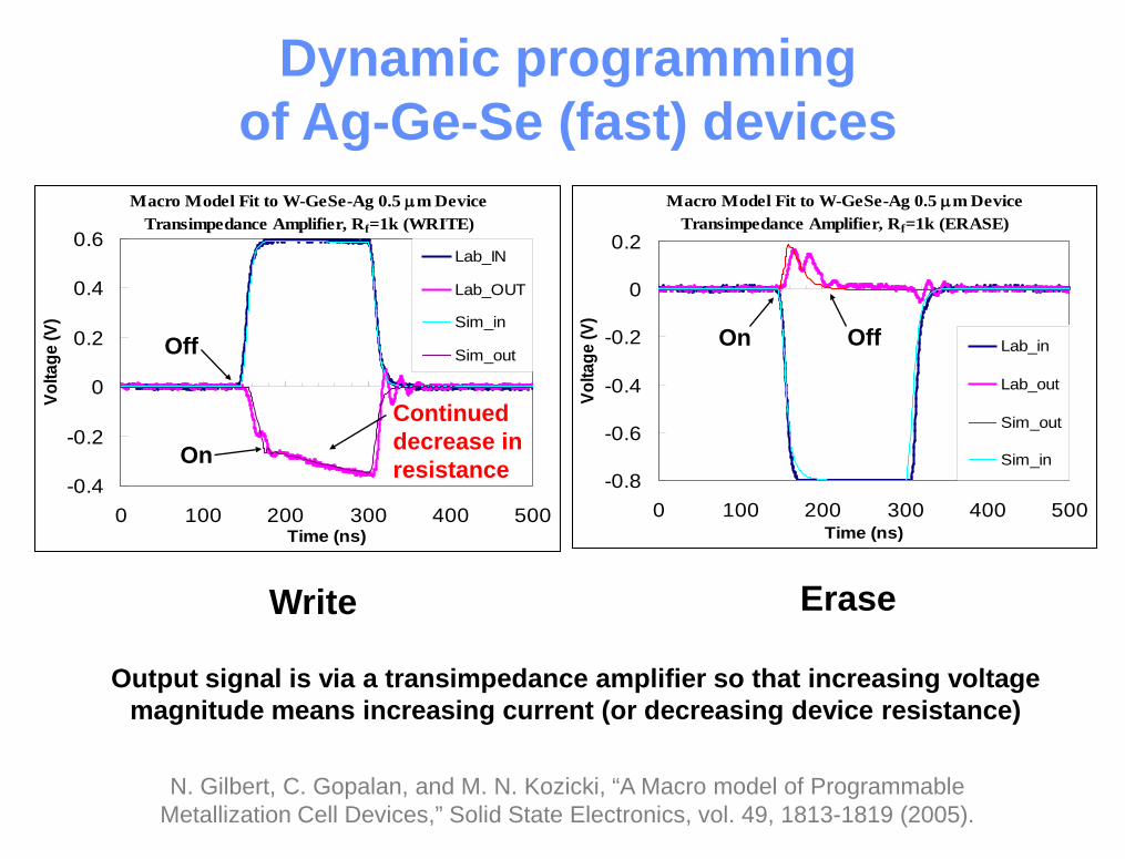
Dynamic programming of Ag-Ge-Se (fast) devices
Macro Model Fit to W-GeSe-Ag 0.5 µm DeviceTransimpedance Amplifier, Rf=1k (WRITE)
-0.4
-0.2
0
0.2
0.4
0.6
0 100 200 300 400 500Time (ns)
Volta
ge (V
)
Lab_IN
Lab_OUT
Sim_in
Sim_out
Write
Off
On
N. Gilbert, C. Gopalan, and M. N. Kozicki, “A Macro model of Programmable Metallization Cell Devices,” Solid State Electronics, vol. 49, 1813-1819 (2005).
Output signal is via a transimpedance amplifier so that increasing voltage magnitude means increasing current (or decreasing device resistance)
Macro Model Fit to W-GeSe-Ag 0.5 µm Device Transimpedance Amplifier, Rf=1k (ERASE)
-0.8
-0.6
-0.4
-0.2
0
0.2
0 100 200 300 400 500Time (ns)
Volta
ge (V
)
Lab_in
Lab_out
Sim_out
Sim_in
Erase
On Off
Continued decrease in resistance
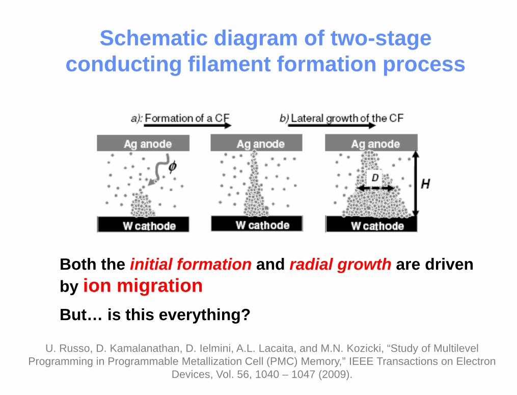
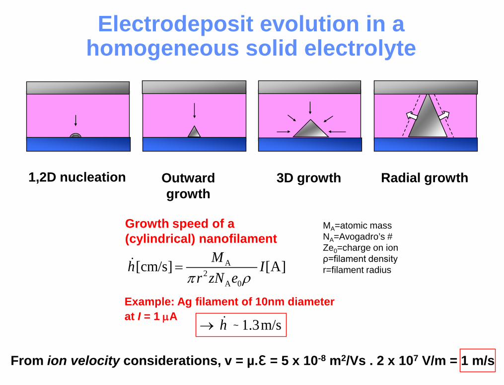
Schematic diagram of two-stage conducting filament formation process
U. Russo, D. Kamalanathan, D. Ielmini, A.L. Lacaita, and M.N. Kozicki, “Study of Multilevel Programming in Programmable Metallization Cell (PMC) Memory,” IEEE Transactions on Electron
Devices, Vol. 56, 1040 – 1047 (2009).
Both the initial formation and radial growth are driven by ion migration But… is this everything?
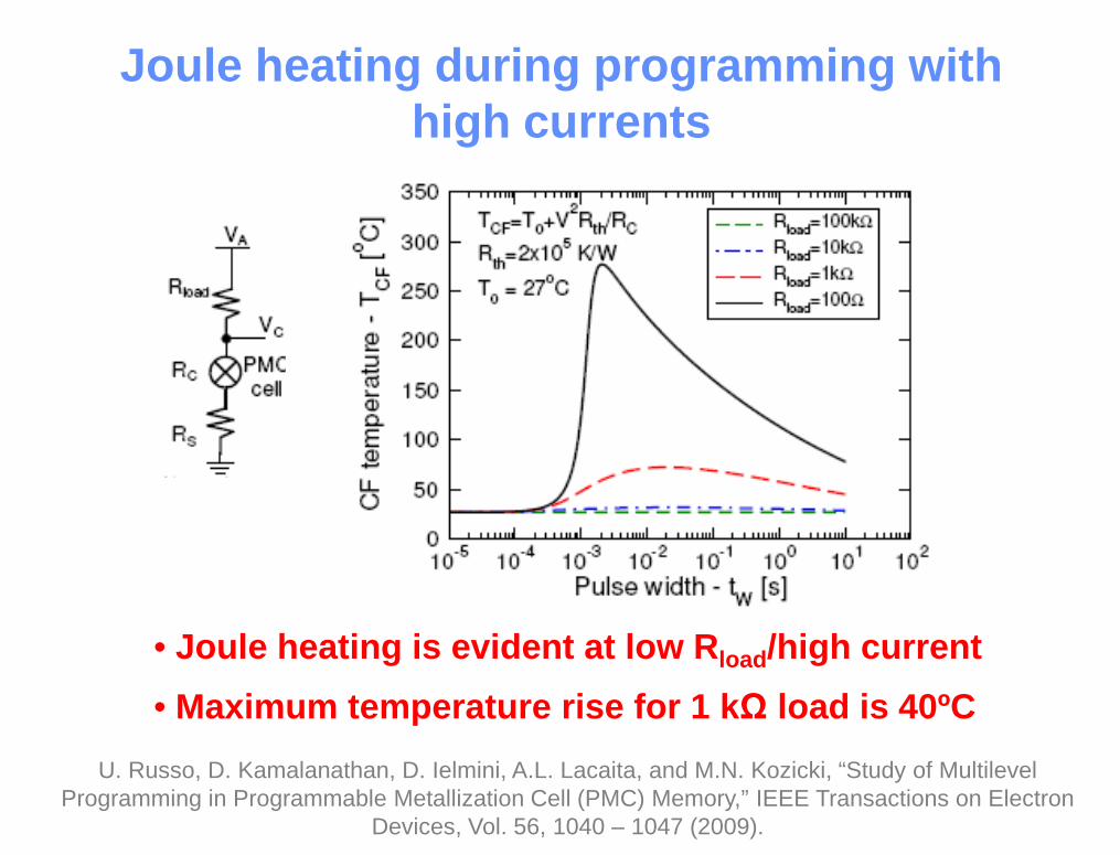
Joule heating during programming with high currents
• Joule heating is evident at low Rload/high current • Maximum temperature rise for 1 kΩ load is 40ºC
U. Russo, D. Kamalanathan, D. Ielmini, A.L. Lacaita, and M.N. Kozicki, “Study of Multilevel Programming in Programmable Metallization Cell (PMC) Memory,” IEEE Transactions on Electron
Devices, Vol. 56, 1040 – 1047 (2009).
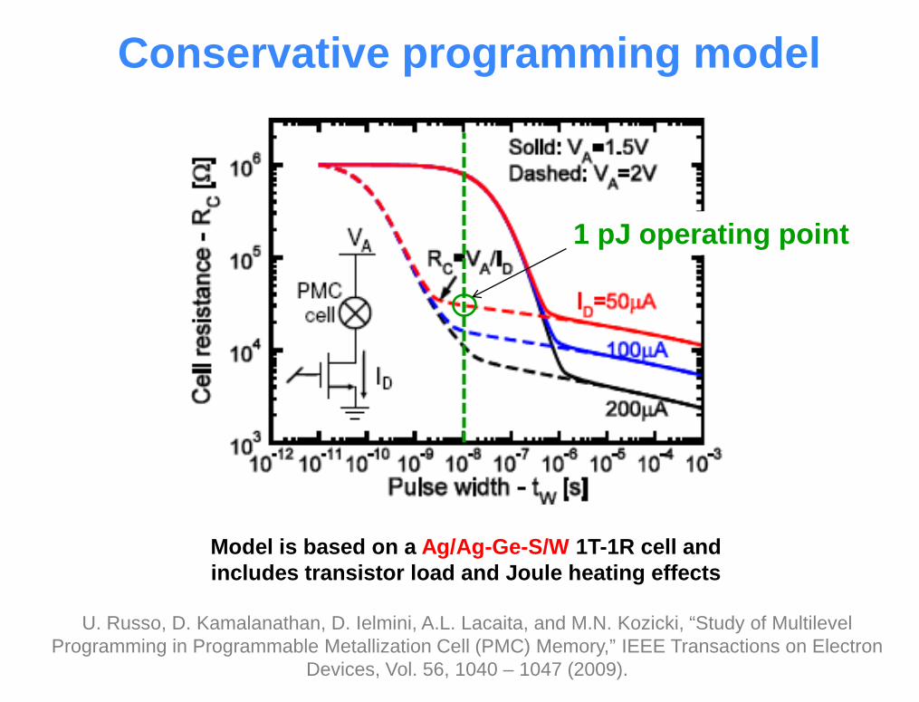
Conservative programming model
U. Russo, D. Kamalanathan, D. Ielmini, A.L. Lacaita, and M.N. Kozicki, “Study of Multilevel Programming in Programmable Metallization Cell (PMC) Memory,” IEEE Transactions on Electron
Devices, Vol. 56, 1040 – 1047 (2009).
1 pJ operating point
Model is based on a Ag/Ag-Ge-S/W 1T-1R cell and includes transistor load and Joule heating effects
D. Kamalanathan, U. Russo, D. Ielmini, and M.N. Kozicki, “Voltage-Driven On–Off Transition and Tradeoff With Program and Erase Current in Programmable Metallization Cell (PMC) Memory,”
IEEE Electron Device Letters, Vol. 30, 553 – 555 (2009).
J.R. Jameson, N. Gilbert, F. Koushan, J. Saenz, J. Wang, S. Hollmer, M. Kozicki, and N. Derhacobian., “Quantized Conductance in Ag/GeS2/W Conductive-Bridge Memory Cells,” IEEE Elec. Dev. Lett., vol. 33, 256-259 (2012).
• Conducting link morphology • Active and passive arrays • The way ahead
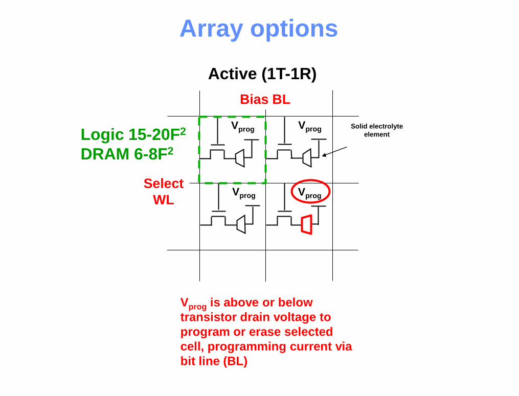
Array options
Vprog Vprog
Vprog Vprog Solid electrolyte element
Active (1T-1R)
Vprog is above or below transistor drain voltage to program or erase selected cell, programming current via bit line (BL)
Select WL
Bias BL
Logic 15-20F2
DRAM 6-8F2
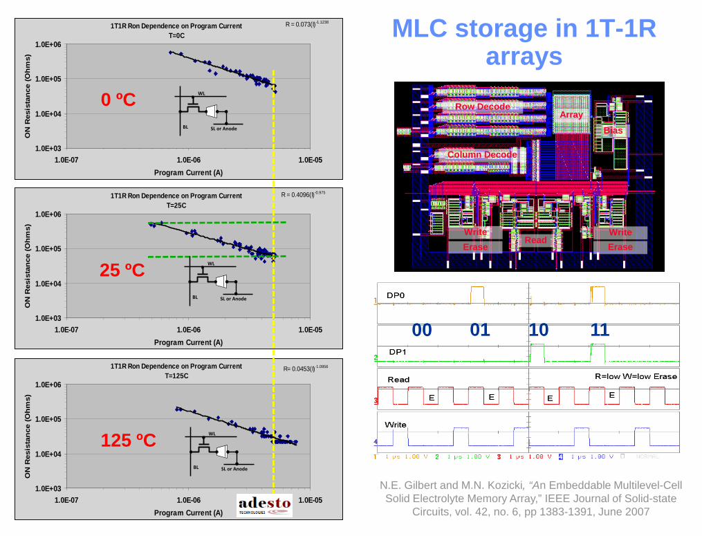
MLC storage in 1T-1R arrays
1T1R Ron Dependence on Program Current T=125C
R= 0.0453(I)-1.0956
1.0E+03
1.0E+04
1.0E+05
1.0E+06
1.0E-07 1.0E-06 1.0E-05Program Current (A)
ON
Res
ista
nce
(Ohm
s)1T1R Ron Dependence on Program Current
T=0CR = 0.073(I)-1.1238
1.0E+03
1.0E+04
1.0E+05
1.0E+06
1.0E-07 1.0E-06 1.0E-05Program Current (A)
ON
Res
ista
nce
(Ohm
s)
1T1R Ron Dependence on Program Current T=25C
R = 0.4096(I)-0.975
1.0E+03
1.0E+04
1.0E+05
1.0E+06
1.0E-07 1.0E-06 1.0E-05Program Current (A)
ON
Res
ista
nce
(Ohm
s)
0 ºC
25 ºC
125 ºC
00 01 10 11
Array Row Decode
Column Decode
Bias
Read Write Write
Erase Erase
N.E. Gilbert and M.N. Kozicki, “An Embeddable Multilevel-Cell Solid Electrolyte Memory Array,” IEEE Journal of Solid-state
Circuits, vol. 42, no. 6, pp 1383-1391, June 2007
SL or Anode
WL
BL
SL or Anode
WL
BL
SL or Anode
WL
BL
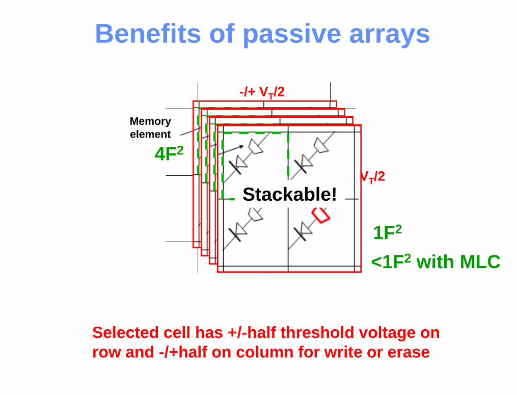
Benefits of passive arrays
Memory element
Selected cell has +/-half threshold voltage on row and -/+half on column for write or erase
+/- VT/2
-/+ VT/2
4F2
Stackable!
1F2
<1F2 with MLC
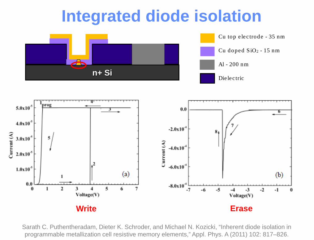
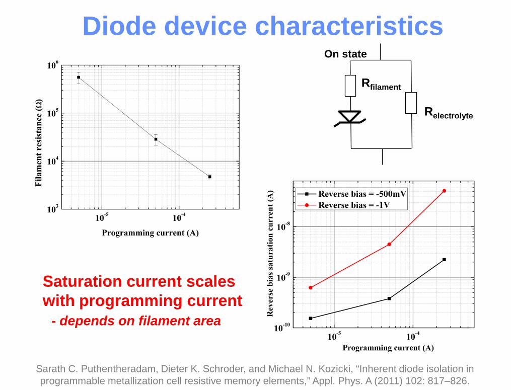
Integrated diode isolation
n+ Si
Sarath C. Puthentheradam, Dieter K. Schroder, and Michael N. Kozicki, “Inherent diode isolation in programmable metallization cell resistive memory elements,” Appl. Phys. A (2011) 102: 817–826.
Cu top e lec trode - 35 nm Cu doped S iO2 - 15 nm Al - 200 nm Die lec tric
Write Erase
Rfilament
Relectrolyte
On state
Saturation current scales with programming current - depends on filament area
Diode device characteristics
Sarath C. Puthentheradam, Dieter K. Schroder, and Michael N. Kozicki, “Inherent diode isolation in programmable metallization cell resistive memory elements,” Appl. Phys. A (2011) 102: 817–826.
• Conducting link morphology • Active and passive arrays • The way ahead
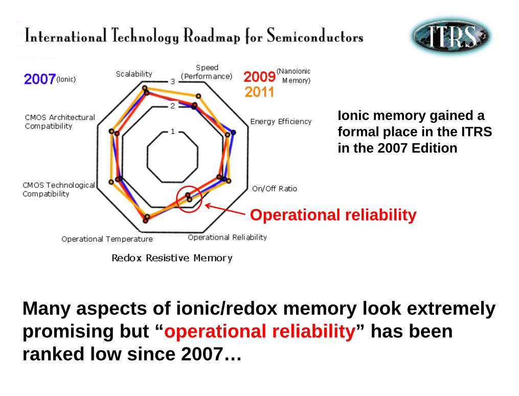
Ionic memory gained a formal place in the ITRS in the 2007 Edition
Many aspects of ionic/redox memory look extremely promising but “operational reliability” has been ranked low since 2007…
Operational reliability
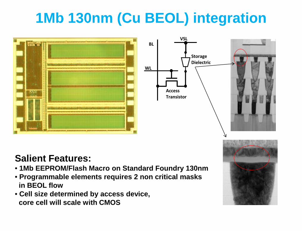
1Mb 130nm (Cu BEOL) integration
Salient Features: • 1Mb EEPROM/Flash Macro on Standard Foundry 130nm • Programmable elements requires 2 non critical masks in BEOL flow • Cell size determined by access device, core cell will scale with CMOS
WL
BL VSL
Storage Dielectric
Access Transistor
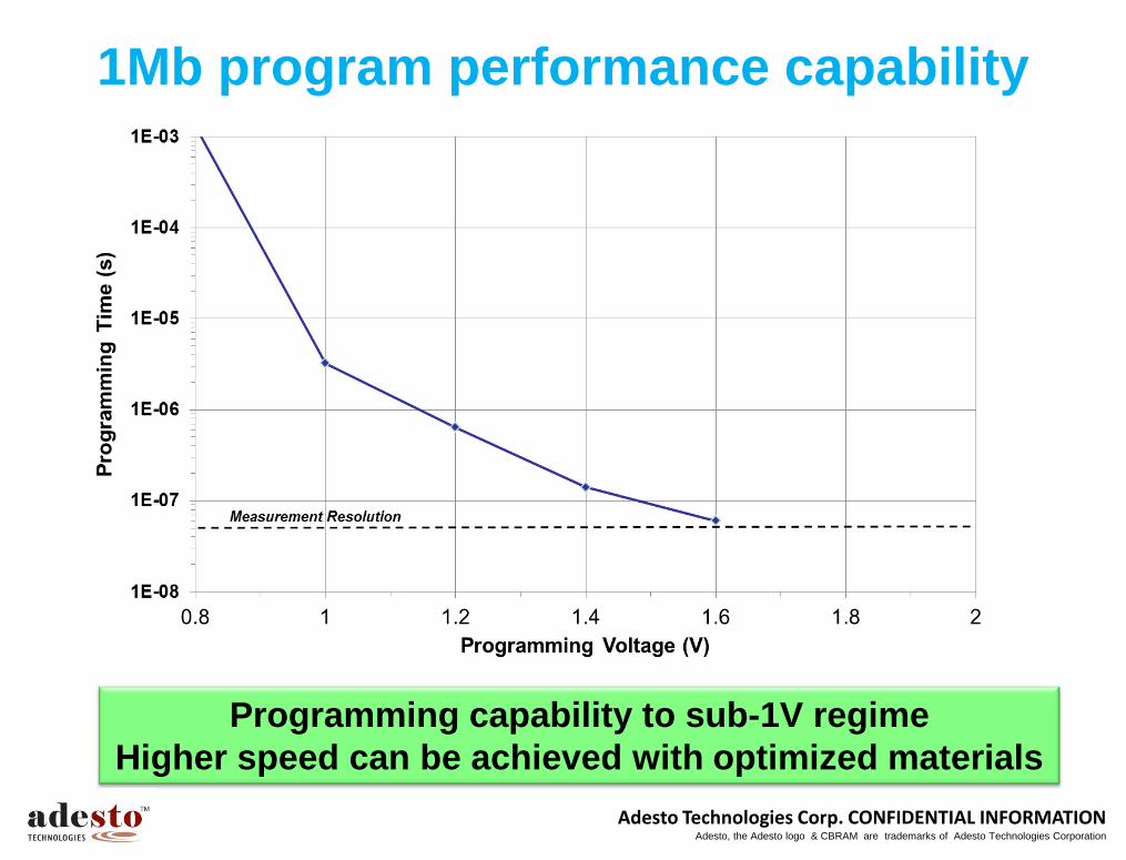
1Mb program performance capability
Programming capability to sub-1V regime Higher speed can be achieved with optimized materials
Adesto Technologies Corp. CONFIDENTIAL INFORMATION Adesto, the Adesto logo & CBRAM are trademarks of Adesto Technologies Corporation
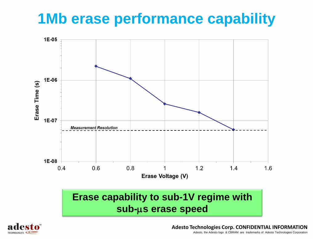
1Mb erase performance capability
Erase capability to sub-1V regime with sub-µs erase speed
Adesto Technologies Corp. CONFIDENTIAL INFORMATION Adesto, the Adesto logo & CBRAM are trademarks of Adesto Technologies Corporation
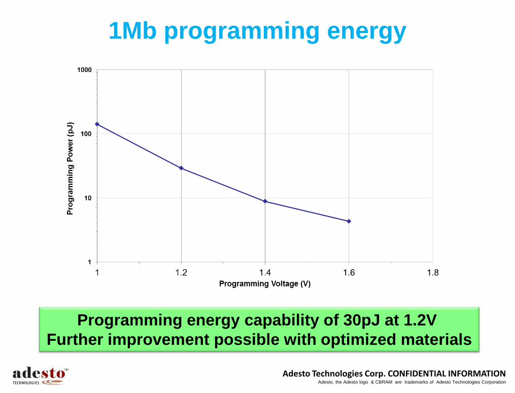
1Mb programming energy
Programming energy capability of 30pJ at 1.2V Further improvement possible with optimized materials
Adesto Technologies Corp. CONFIDENTIAL INFORMATION Adesto, the Adesto logo & CBRAM are trademarks of Adesto Technologies Corporation
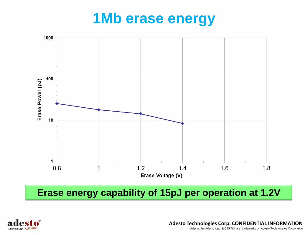
1Mb erase energy
Erase energy capability of 15pJ per operation at 1.2V
Adesto Technologies Corp. CONFIDENTIAL INFORMATION Adesto, the Adesto logo & CBRAM are trademarks of Adesto Technologies Corporation
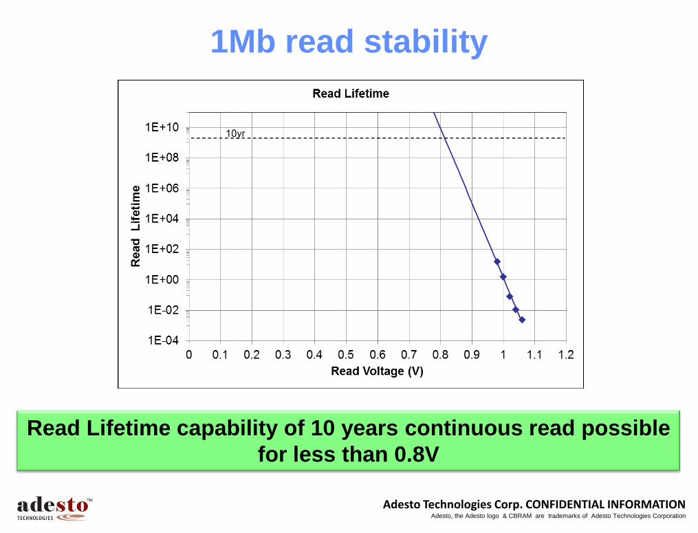
1Mb read stability
Read Lifetime capability of 10 years continuous read possible for less than 0.8V
Adesto Technologies Corp. CONFIDENTIAL INFORMATION Adesto, the Adesto logo & CBRAM are trademarks of Adesto Technologies Corporation