Copyright Cirrus Logic, Inc. 2014 (All Rights Reserved) http://www.cirrus.com Evaluation Board for CS42L56 Features Analog Line and Microphone Level Inputs – 6 RCA and 3 Stereo 1/8” Jacks – Compatible with Single-Ended and Pseudo-Diff. Input Configurations Analog Line and Headphone Outputs – Stereo 1/8” Headphone Jack w/Input Detection – 4 RCA Jacks for Headphone/Line Outputs 8 to 96 kHz S/PDIF Interface – CS8416 Digital Audio Receiver – CS8406 Digital Audio Transmitter I/O Stake Header Accessibility – External Control Port Headers – External Direct and Buffered Serial Audio I/O Headers Multiple Power Supply options via USB, Battery or External Power Supplies. 1.8 V to 3.3 V Selectable Logic Interface FlexGUI S/W Control - Windows ® Compatible – Pre-Defined & User-Configurable Scripts Description The CDB42L56 is the ideal evaluation platform solution to test and evaluate the CS42L56.The CS42L56 is a highly integrat- ed, 24-bit, ultra-low power stereo codec based on multi-bit delta-sigma modulation suitable for low power portable appli- cations. Use of the board requires an analog/digital signal source, an analyzer and power supplies. A Windows PC-com- patible computer is also needed in order to configure the CS42L56 and the board. System timing can be provided by the CS8416 (on-board), by the CS42L56 supplied with a master clock, by the on-board crystal oscillator or via an I/O stake header with a DSP connected. RCA phono connectors and stereo 1/8 th inch audio jacks are provided for CS42L56 analog inputs and HP/Line outputs. Digital I/O connections are provided via RCA phono or optical connectors to the CS8416 and CS8406 (S/PDIF Rx and Tx). The CDB42L56 is programmed via the PC’s USB using Cirrus Logic’s Microsoft ® Windows ® -based software (FlexGUI). The evaluation board may also be configured to accept external timing and data signals for operation in a user application during system development. ORDERING INFORMATION CDB42L56 Evaluation Board USB μ controller CS42L56 S/PDIF Rx (CS8416) S/PDIF Tx (CS8406) FPGA Oscillator (socket) I 2 C Interface Reset Reset PLL Tx SRC (CS8421) Analog Outputs (Line + Headphone) Analog Inputs (Line + MIC) External System I/O Header Rx SRC (CS8421) PSIA I/O Header USB/ RS232 S/PDIF Dout S/PDIF Din FEB '14 DS851DB1 CDB42L56
Transcript
CDB42L56
Evaluation Board for CS42L56
Features
Analog Line and Microphone Level Inputs– 6 RCA and 3 Stereo 1/8” Jacks
– Compatible with Single-Ended and Pseudo-Diff. Input Configurations
Analog Line and Headphone Outputs– Stereo 1/8” Headphone Jack w/Input Detection
– 4 RCA Jacks for Headphone/Line Outputs
8 to 96 kHz S/PDIF Interface– CS8416 Digital Audio Receiver
– CS8406 Digital Audio Transmitter
I/O Stake Header Accessibility– External Control Port Headers
– External Direct and Buffered Serial Audio I/O Headers
Multiple Power Supply options via USB, Battery or External Power Supplies.
1.8 V to 3.3 V Selectable Logic Interface
FlexGUI S/W Control - Windows® Compatible– Pre-Defined & User-Configurable Scripts
Description
The CDB42L56 is the ideal evaluation platform solution to testand evaluate the CS42L56.The CS42L56 is a highly integrat-ed, 24-bit, ultra-low power stereo codec based on multi-bitdelta-sigma modulation suitable for low power portable appli-cations. Use of the board requires an analog/digital signalsource, an analyzer and power supplies. A Windows PC-com-patible computer is also needed in order to configure theCS42L56 and the board.
System timing can be provided by the CS8416 (on-board), bythe CS42L56 supplied with a master clock, by the on-boardcrystal oscillator or via an I/O stake header with a DSPconnected.
RCA phono connectors and stereo 1/8th inch audio jacks areprovided for CS42L56 analog inputs and HP/Line outputs.Digital I/O connections are provided via RCA phono or opticalconnectors to the CS8416 and CS8406 (S/PDIF Rx and Tx).
The CDB42L56 is programmed via the PC’s USB using CirrusLogic’s Microsoft® Windows®-based software (FlexGUI). Theevaluation board may also be configured to accept externaltiming and data signals for operation in a user applicationduring system development.
ORDERING INFORMATION
CDB42L56 Evaluation Board
USB µ controller
CS42L56
S/PDIF Rx (CS8416)
S/PDIF Tx (CS8406)
FPGA
Oscillator (socket)
I2C Interface
Reset
Reset
PLL
Tx SRC(CS8421)
Analog Outputs(Line + Headphone)
Analog Inputs(Line + MIC)
External System I/O Header
Rx SRC(CS8421)
PSIA I/O Header
USB/ RS232
S/PDIF Dout
S/PDIF Din
Copyright Cirrus Logic, Inc. 2014(All Rights Reserved)
TABLE OF CONTENTS1. SYSTEM OVERVIEW ............................................................................................................................. 4
1.1 Control Port and Board Configuration .............................................................................................. 41.2 Power ............................................................................................................................................... 41.3 Digital Input ....................................................................................................................................... 4
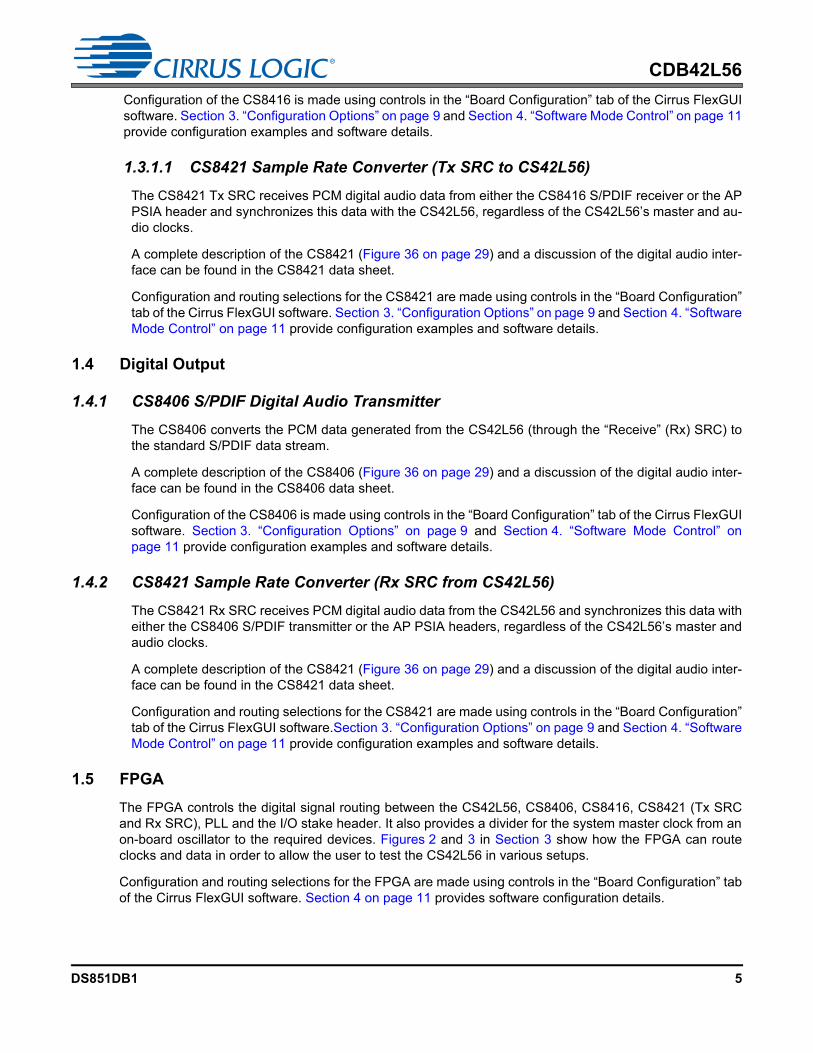
1.3.1 CS8416 S/PDIF Digital Audio Receiver .................................................................................. 41.3.1.1 CS8421 Sample Rate Converter (Tx SRC to CS42L56) ............................................. 5
1.4 Digital Output .................................................................................................................................... 51.4.1 CS8406 S/PDIF Digital Audio Transmitter .............................................................................. 51.4.2 CS8421 Sample Rate Converter (Rx SRC from CS42L56) .................................................... 5
3.1 S/PDIF In to Analog Out and Analog In to S/PDIF Out .................................................................... 93.2 PSIA In to Analog Out and Analog In to PSIA Out ......................................................................... 10
5. JUMPER SETTINGS AND SYSTEM CONNECTIONS ........................................................................ 186. PERFORMANCE PLOTS ..................................................................................................................... 217. CDB42L56 BLOCK DIAGRAM ............................................................................................................ 278. CDB42L56 SCHEMATICS ................................................................................................................... 289. CDB42L56 LAYOUT ............................................................................................................................ 3310. REVISION HISTORY .......................................................................................................................... 38
LIST OF FIGURESFigure 1. Quick-Start Board Layout ............................................................................................................. 8Figure 2. S/PDIF In to Analog Out and Analog In to S/PDIF Out ................................................................ 9Figure 3. PSIA In to Analog Out and Analog In to PSIA Out ..................................................................... 10Figure 4. Board Configuration Tab ............................................................................................................ 12Figure 5. Codec Configuration Tab ........................................................................................................... 13Figure 6. Codec Analog Input Volume Tab ............................................................................................... 14Figure 7. Codec DSP Engine Tab ............................................................................................................. 15Figure 8. Codec Analog Output Volume Tab ............................................................................................ 16Figure 9. Register Maps Tab - CS42L56 .................................................................................................. 17Figure 10. THD+N vs. Freq. - Analog In to Digital Out .............................................................................. 21Figure 11. THD+N vs. Amplitude - Analog In to Digital Out ...................................................................... 21Figure 12. FFT - Analog In to Digital Out @ -1 dBFS ............................................................................... 21Figure 13. FFT - Analog In to Digital Out @ -60 dBFS ............................................................................. 21Figure 14. FFT - Analog In to Digital Out - No Input ................................................................................. 22Figure 15. FFT Crosstalk - Analog In to Digital Out@ -1 dBFS ................................................................................................................................................ 22Figure 16. Freq. Response - Analog In to Digital Out ............................................................................... 22
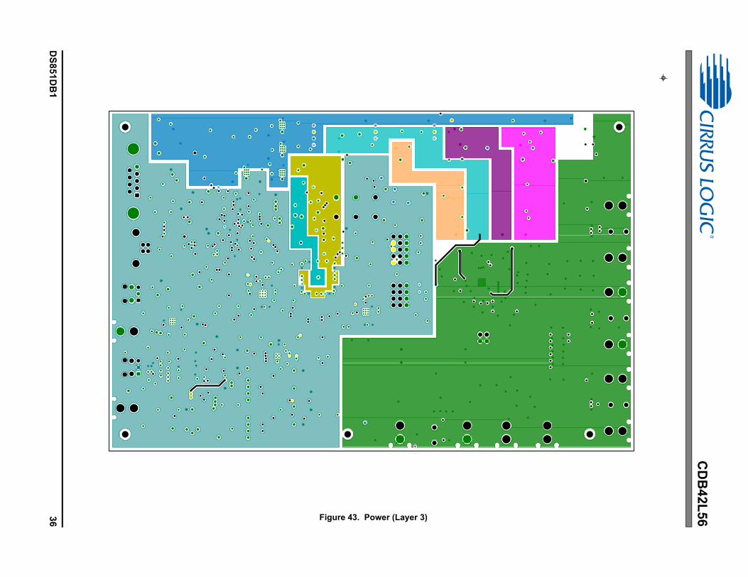
Figure 17. Fade-to-Noise Linearity - Analog In to Digital Out ................................................................... 22Figure 18. THD+N vs. Freq. - Digital In to HP Out .................................................................................... 22Figure 19. THD+N vs. Amplitude - Digital In to HP Out ............................................................................ 22Figure 20. THD+N vs. Volume - Digital In to HP Out ................................................................................ 23Figure 21. FFT - Digital In to HP Out @ 0 dBFS ....................................................................................... 23Figure 20. FFT - Digital In to HP Out @ -60 dBFS .................................................................................... 23Figure 21. FFT - Digital In to HP Out - No Input ........................................................................................ 23Figure 22. FFT - Digital In to HP Out - No Input Wideband ...................................................................... 23Figure 23. FFT Crosstalk - Digital In to HP Out @ 0 dBFS ....................................................................... 23Figure 24. Freq. Response - Digital In to HP Out ..................................................................................... 24Figure 25. Fade-to-Noise Linearity- Digital In to HP Out ........................................................................... 24Figure 26. THD+N vs. Freq. - Digital In to Line Out .................................................................................. 24Figure 27. THD+N vs. Amplitude - Digital In to Line Out .......................................................................... 24Figure 28. THD+N vs. Volume - Digital In to Line Out .............................................................................. 25Figure 29. FFT Crosstalk - Digital In to Line Out @ 0 dBFS ..................................................................... 25Figure 28. FFT - Digital In to Line Out @ 0 dBFS ..................................................................................... 25Figure 29. FFT - Digital In to Line Out @ -60 dBFS .................................................................................. 25Figure 30. FFT - Digital In to Line Out - No Input ...................................................................................... 25Figure 31. FFT - Digital In to Line Out - No Input Wideband ..................................................................... 25Figure 32. Freq. Response - Digital In to Line Out .................................................................................... 26Figure 33. Fade-to-Noise Linearity- Digital In to Line Out ......................................................................... 26Figure 34. Block Diagram .......................................................................................................................... 27Figure 35. CS42L56 & Analog I/O (Schematic Sheet 1) ........................................................................... 28Figure 36. S/PDIF & Digital Interface (Schematic Sheet 2) ...................................................................... 29Figure 37. PLL, oscillator and external I/O connections (Schematic Sheet 3) .......................................... 30Figure 38. Microcontroller and FPGA (Schematic Sheet 4) ...................................................................... 31Figure 39. Power (Schematic Sheet 5) ..................................................................................................... 32Figure 40. Silk Screen ............................................................................................................................... 33Figure 41. Top-Side Layer ........................................................................................................................ 34Figure 42. GND (Layer 2) .......................................................................................................................... 35Figure 43. Power (Layer 3) ....................................................................................................................... 36Figure 44. Bottom Side Layer ................................................................................................................... 37
LIST OF TABLESTable 1. Analog Input Configuration Jumper and Resistor Settings ........................................................... 7Table 2. System Connections ................................................................................................................... 18Table 3. Jumper Settings .......................................................................................................................... 19
The CDB42L56 evaluation platform provides analog and digital interfaces to the CS42L56 and allows for externalDSP and I²C interconnects to the board. On-board peripherals are powered either from the USB connection or froman external +5 V supply. On-board voltage regulators provide power to the digital and analog cores of the CS42L56.The CDB42L56 is configured using Cirrus Logic’s Windows-compatible FlexGUI software to read/write to deviceregisters.
This section describes the various components on the CDB42L56 and how they are used with the CS42L56. Section2 on page 8 is a simplified quick connect guide provided for user convenience and may be used to quickly configurethe CS42L56. Section 3 on page 9 describes some of the configurations available for transmitting and receiving au-dio signals. Section 4 on page 11 provides software configuration details. Section 5 on page 18 provides a descrip-tion of all stake headers and connectors, including the default factory settings of all jumpers. Section 6 on page 21provides typical performance plots. The CDB42L56 schematic and layout set is shown in Figures 35 through 44.
1.1 Control Port and Board Configuration
The CDB42L56 evaluation board must be programmed using the Windows compatible software (Cirrus Log-ic FlexGUI) provided. This software allows the user to program the registers of all the programmable com-ponents on the board using an I²C interface.
The GUI interfaces with an on-board micro controller through either the USB or the serial port connector.For a detailed explanation on software controls, refer to Section 4 on page 11.
Alternatively, the I²C interface to the CS42L56 can be directly accessed through an I/O header (J109) toaccept external timing and signals in a user application during system development.
1.2 Power
Power is supplied to the evaluation board through either the +5.0 V test points or the VBUS supply from theUSB. NOTE: The minimum current required for board operation is approximately 300 mA. It may thereforebe necessary to connect the CDB42L56 directly to the USB port on the PC as opposed to a hub or keyboardport where the current might be limited.
Jumpers connect the CS42L56’s supplies to a low dropout regulated voltage of +1.8 V, +2.5 V or +3.3 V forVL and +1.8 V or +2.5 V for VLDO, VA and VCP. A selection for a 1.8 V supply from a buck regulator is alsoavailable, providing a more efficient means of evaluating the CS42L56’s performance when powered frombatteries (3 AAA battery connectors are available on the bottom side of the CDB).
For current measurement purposes only, a 1 ohm series resistor is connected to each supply. The currentis easily calculated by measuring the voltage drop across this resistor. NOTE: The stake headers connectedin parallel with these resistors must be shunted with the supplied jumper during normal operation.
WARNING: Please refer to the CS42L56 data sheet for allowable voltage levels.
1.3 Digital Input
1.3.1 CS8416 S/PDIF Digital Audio Receiver
The CS8416 S/PDIF receiver converts an incoming S/PDIF data input stream into PCM data for theCS42L56 (through the “Transmit” (Tx) Sample Rate Converter (SRC)).
A complete description of the CS8416 (Figure 36 on page 29) and a discussion of the digital audio inter-face can be found in the CS8416 data sheet.
Configuration of the CS8416 is made using controls in the “Board Configuration” tab of the Cirrus FlexGUIsoftware. Section 3. “Configuration Options” on page 9 and Section 4. “Software Mode Control” on page 11provide configuration examples and software details.
1.3.1.1 CS8421 Sample Rate Converter (Tx SRC to CS42L56)
The CS8421 Tx SRC receives PCM digital audio data from either the CS8416 S/PDIF receiver or the APPSIA header and synchronizes this data with the CS42L56, regardless of the CS42L56’s master and au-dio clocks.
A complete description of the CS8421 (Figure 36 on page 29) and a discussion of the digital audio inter-face can be found in the CS8421 data sheet.
Configuration and routing selections for the CS8421 are made using controls in the “Board Configuration”tab of the Cirrus FlexGUI software. Section 3. “Configuration Options” on page 9 and Section 4. “SoftwareMode Control” on page 11 provide configuration examples and software details.
1.4 Digital Output
1.4.1 CS8406 S/PDIF Digital Audio Transmitter
The CS8406 converts the PCM data generated from the CS42L56 (through the “Receive” (Rx) SRC) tothe standard S/PDIF data stream.
A complete description of the CS8406 (Figure 36 on page 29) and a discussion of the digital audio inter-face can be found in the CS8406 data sheet.
Configuration of the CS8406 is made using controls in the “Board Configuration” tab of the Cirrus FlexGUIsoftware. Section 3. “Configuration Options” on page 9 and Section 4. “Software Mode Control” onpage 11 provide configuration examples and software details.
1.4.2 CS8421 Sample Rate Converter (Rx SRC from CS42L56)
The CS8421 Rx SRC receives PCM digital audio data from the CS42L56 and synchronizes this data witheither the CS8406 S/PDIF transmitter or the AP PSIA headers, regardless of the CS42L56’s master andaudio clocks.
A complete description of the CS8421 (Figure 36 on page 29) and a discussion of the digital audio inter-face can be found in the CS8421 data sheet.
Configuration and routing selections for the CS8421 are made using controls in the “Board Configuration”tab of the Cirrus FlexGUI software.Section 3. “Configuration Options” on page 9 and Section 4. “SoftwareMode Control” on page 11 provide configuration examples and software details.
1.5 FPGA
The FPGA controls the digital signal routing between the CS42L56, CS8406, CS8416, CS8421 (Tx SRCand Rx SRC), PLL and the I/O stake header. It also provides a divider for the system master clock from anon-board oscillator to the required devices. Figures 2 and 3 in Section 3 show how the FPGA can routeclocks and data in order to allow the user to test the CS42L56 in various setups.
Configuration and routing selections for the FPGA are made using controls in the “Board Configuration” tabof the Cirrus FlexGUI software. Section 4 on page 11 provides software configuration details.
The socketed on-board oscillator (Y1) can be selected as the system master clock source by using the se-lections on the “Board Configuration” tab of the Cirrus FlexGUI. Section 4 on page 11 provides softwareconfiguration details.
The oscillator is mounted in pin sockets, allowing easy removal or replacement. The device footprint on theboard will accommodate half-can or full-can sized oscillators.
1.7 PLL
An on-board PLL is used with the FPGA to generate the serial port sub-clocks for the CS42L56’s serial portwhen the CS42L56 is set to slave mode. The sub-clocks’ frequencies are selected on the “Board Configu-ration” tab of the Cirrus FlexGUI. Section 4 on page 11 provides software configuration details.
1.8 I/O Stake Headers
Headers J104 and J109 (Figure 35 on page 28) provide unbuffered bidirectional access to the CS42L56serial port and control port, respectively. For regular operation, the left two pins on all rows should be shunt-ed to allow the CS42L56 to receive serial and control port data and clocks from the on-board FPGA.
Alternatively, the stake headers provide access to the CS42L56 from external systems simply by removingall the shunt jumpers from the “USB” and “CDB I/O” positions. The user may then connect a ribbon cableconnector to the “Ext. Sys. Connect” pins for external control of board functions. A single row of “GND” pinsis provided to maintain signal ground integrity. Two unpopulated pull-up resistors are also available shouldthe user choose to use the CDB42L56 logic supply (VL) externally.
If an external system is used to interface with the CS42L56 through headers J104 and J109, the digital I/Ologic voltage levels must be selected cautiously since the lines between the headers and the device are notbuffered. Please refer to the CS42L56 product data sheet for a detailed explanation on digital I/O interfacespecifications. Selections are made using the “Board Configuration” tab of the Cirrus FlexGUI software.Section 4 on page 11 provides software configuration details.
1.9 CS42L56 Audio Codec
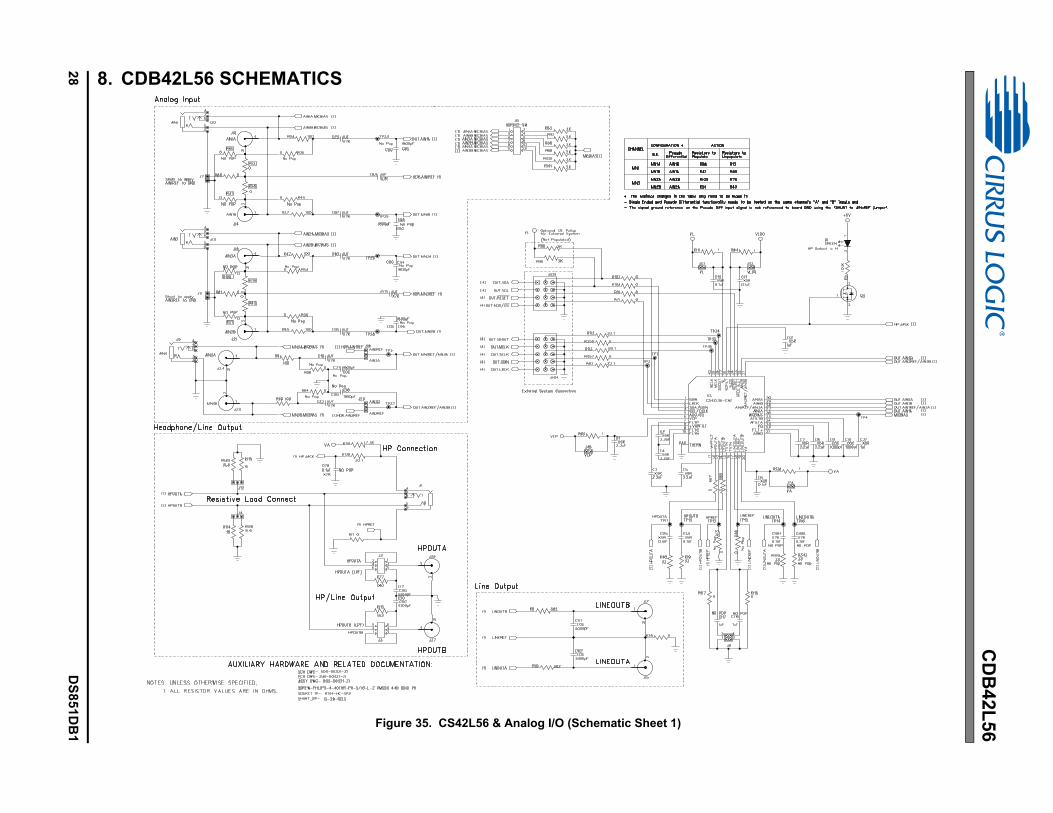
A complete description of the CS42L56 (U3 - Figure 35 on page 28) can be found in the CS42L56 productdata sheet.
The CS42L56 is configured using the Cirrus Logic Windows compatible software FlexGUI. The device con-figuration registers are directly accessible via the “Register Maps” tab of the Cirrus FlexGUI software. Thistab provides low-level control of each bit. For easier configuration, additional tabs provide high-level control.Section 4 on page 11 provides software configuration details.
1.10 Analog Inputs
The analog input circuitry on the CDB42L56 has been designed to allow for testing of the CS42L56 in all itspossible analog input configurations. Line or microphone level analog input signals can be provided to theanalog inputs on the CS42L56 through RCA or microphone input jacks (Figure 35 on page 28). Stake head-er J6 allows the user to select (with jumpers installed) the CS42L56 as the microphone bias source for eachmicrophone input (CAUTION: Only 2 jumpers may be installed at a time).
Headers J19 and J20 are used to select the desired input for pins AIN3A/AIN1REF and AIN3B/AIN2REFon the CS42L56. These headers can be used to select between either a single-ended or a pseudo-differ-ential analog input setup. Table 1 provides jumper and resistor settings for the various analog input config-urations allowed on the CS42L56. The shaded rows in the table indicate the most commonly usedconfigurations and do not require any extra resistor modifications.
1. Use headers J7 and J11 to select input signal ground reference (in pseudo-differential mode) as eitherthe CDB42L56 board ground or the signal ground reference from the external system which theCDB42L56 receives through the shield of the analog input cable.
2. Resistor modifications are only required if single-ended and pseudo-differential input configurationsneed to be used simultaneously on the “A” and “B” inputs of the same analog input channel.
3. Resistor population settings for resistors not shown in the table should be the same as factory defaults.
Figure 35 on page 28 illustrates how the analog inputs are connected and routed. Table 3 on page 19 de-tails the jumper selections.
1.11 Analog Outputs
The CS42L56 analog outputs can be monitored on RCA jacks J15 and J17 for line and J37 and J38 forheadphone outputs. Additionally, the CS42L56 headphone outputs can also be monitored on stereo head-phone jack J1 which also allows the user to test the CS42L56’s headphone detect functionality. TheCDB42L56 on-board circuitry drives the headphone detect pin low when a headphone is inserted in J1.
Headers J12 and J4 can be used to select optional 16 or 32 resistive loads for headphone outputs.Headers J2 and J3 give users the option of receiving filtered or unfiltered outputs on the RCA headphoneoutput jacks.
Figure 35 on page 28 illustrates how the analog outputs are connected and routed. Table 3 on page 19 pro-vides details on jumper selections for filtered or unfiltered outputs.
No. Analog Input 1 Analog Input 2 Analog Input 3 Jumper Settings Resistors to Populate
Resistors to UnpopulateAIN1A AIN1B AIN2A AIN2B AIN3A AIN3B J19 J20
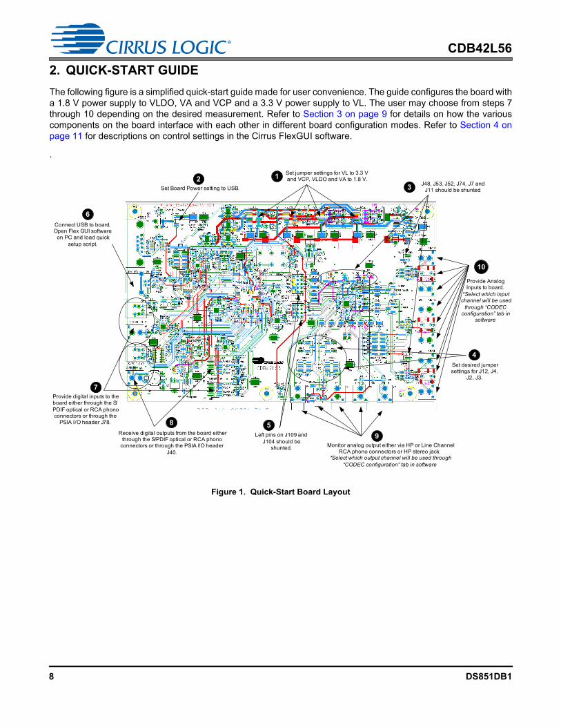
The following figure is a simplified quick-start guide made for user convenience. The guide configures the board witha 1.8 V power supply to VLDO, VA and VCP and a 3.3 V power supply to VL. The user may choose from steps 7through 10 depending on the desired measurement. Refer to Section 3 on page 9 for details on how the variouscomponents on the board interface with each other in different board configuration modes. Refer to Section 4 onpage 11 for descriptions on control settings in the Cirrus FlexGUI software.
.
Figure 1. Quick-Start Board Layout
123
4
5
6
7
Set jumper settings for VL to 3.3 V and VCP, VLDO and VA to 1.8 V.
J48, J53, J52, J74, J7 and J11 should be shunted.Set Board Power setting to USB.
Left pins on J109 and J104 should be
shunted.
Provide digital inputs to the board either through the S/PDIF optical or RCA phono connectors or through the
PSIA I/O header J78.
Receive digital outputs from the board either through the S/PDIF optical or RCA phono
connectors or through the PSIA I/O header J40.
Monitor analog output either via HP or Line Channel RCA phono connectors or HP stereo jack.
*Select which output channel will be used through “CODEC configuration” tab in software
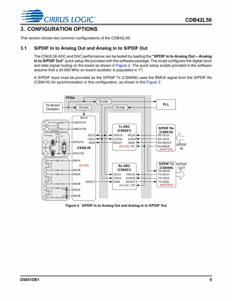
This section shows two common configurations of the CDB42L56.
3.1 S/PDIF In to Analog Out and Analog In to S/PDIF Out
The CS42L56 ADC and DAC performance can be tested by loading the “SPDIF In to Analog Out -- AnalogIn to S/PDIF Out” quick setup file provided with the software package. The script configures the digital clockand data signal routing on the board as shown in Figure 2. The quick setup scripts provided in the softwareassume that a 24.000 MHz on-board oscillator is populated in Y1.
A S/PDIF input must be provided as the S/PDIF Tx (CS8406) uses the RMCK signal from the S/PDIF Rx(CS8416) for synchronization in this configuration, as shown in the Figure 2.
Line OutputB
A
HP Output J21
32
32
16
16
J4
J12
B
A
AIN1A
AIN1B
AIN2A
AIN2B
AIN3A
AIN3B
J19
J20
LRCK
CS42L56
SCLK
SDIN
(SLAVE)
MCLK
SDOUT
LINEOUTB
LINEOUTA
HPOUTB
HPOUTA
AIN1A
AIN1B
AIN2A
AIN2B
AIN3A
AIN3B
S/PDIF Rx (CS8416)
RX.LRCK
RX.SCLK
RX.SDOUTS/PDIF
IN(MASTER)RX.RMCK
TX.SCLK
TX.LRCKTX.SDIN
S/PDIF OUT
(MASTER)
S/PDIF Tx (CS8406)
TX.OMCK
FPGA
PLLDivider
DividerDividerOn-BoardOscillator
Tx SRC(CS8421)
(SLAVE)
ISCLK
ILRCKSDIN
OSCLK
OLRCKSDOUT
XTI
Rx SRC(CS8421)
(SLAVE)
ISCLK
ILRCKSDIN
OSCLK
OLRCKSDOUT
XTI
Figure 2. S/PDIF In to Analog Out and Analog In to S/PDIF Out
3.2 PSIA In to Analog Out and Analog In to PSIA Out
The CS42L56 ADC and DAC performance can be tested by loading the “PSIA In to Analog Out -- AnalogIn to PSIA Out” quick setup file provided with the software package. The script configures the digital clockand data signal routing on the board as shown in Figure 2. The quick setup scripts provided in the softwareassume that a 24.000 MHz on-board oscillator is populated in Y1.
Line OutputB
A
HP Output J21
32
32
16
16
J4
J12
B
A
AIN1A
AIN1B
AIN2A
AIN2B
AIN3A
AIN3B
J19
J20
LRCK
CS42L56
SCLK
SDIN
(SLAVE)
MCLK
SDOUT
LINEOUTB
LINEOUTA
HPOUTB
HPOUTA
AIN1A
AIN1B
AIN2A
AIN2B
AIN3A
AIN3B
FPGA
PLLDivider
DividerDividerOn-BoardOscillator
Tx SRC(CS8421)
(SLAVE)
ISCLK
ILRCKSDIN
OSCLK
OLRCKSDOUT
XTI
PSIA Tx (J78)
TX.SCLKTX.LRCKTX.SDOUT
PSIA Rx (J40)RX.SCLKRX.LRCKRX.SDIN
TX.MCLK
RX.MCLK
Rx SRC(CS8421)
(SLAVE)
ISCLK
ILRCKSDIN
OSCLK
OLRCKSDOUT
XTI
(MASTER)
(MASTER)
Figure 3. PSIA In to Analog Out and Analog In to PSIA Out
The CDB42L56 may be used with the Microsoft® Windows®-based FlexGUI graphical user interface, allowing soft-ware control of the CS42L56, FPGA, CS8421, CS8416 and CS8406 registers. The latest control software may bedownloaded from www.cirrus.com/msasoftware. Step-by-step instructions for setting up the FlexGUI are providedas follows:
1. Download and install the FlexGUI software as instructed on the web site.
2. Connect the CDB to the host PC using a USB cable.
3. Launch the Cirrus FlexGUI. Once the GUI is launched successfully, all registers are set to their default resetstate.
4. Refresh the GUI by clicking on the “Update” button. The default state of all registers are now visible.
For standard set-up:
5. Set up the signal routing in the “Board Configuration” tab as desired.
6. Set up the CS42L56 in the “Codec Configuration”, “Codec Analog Input Volume”, “Codec DSP Engine”, “Co-dec Analog Output Volume” and “Register Maps” tabs as desired.
7. Begin evaluating the CS42L56.
For quick set-up, the CDB42L56 may, alternatively, be configured by loading a predefined sample script file:
8. On the File menu, click "Restore Board Registers..."
9. Browse to Boards\CDB42L56\Scripts\.
10. Choose any one of the provided scripts to begin evaluation.
To create personal scripts files:
11. On the File menu, click “Save Board Registers...”
12. Enter any name that sufficiently describes the created setup.
13. Choose the desired location and save the script.
14. To load this script, follow the instructions from step 8 above.
The “Board Configuration” tab provides high-level control of signal routing on the CDB42L56. The controlsin this tab are used to setup the CS8416, CS8406, Tx SRC, Rx SRC and the FPGA routing and are dividedinto separate control groups for each of these individual devices. A description of each control group is out-lined below. This tab also includes a drop down menu with a list of quick-setup configurations. Selecting aquick-setup from the drop down box, the software loads a predefined configuration for the different deviceson the board. Section 3 on page 9 provides details on some quick-setup configurations.
FPGA Routing - Includes controls to setup the FPGA for using the S/PDIF or the PSIA test interface and forsetting up clock and signal routing for CS42L56 in master/slave mode. This group also has controls for se-lecting SCLK and LRCK frequencies, perform divide operations on the oscillator.
CS8416 S/PDIF Receiver Control - Controls for the CS8416.
CS8406 S/PDIF Transmitter Control - Controls for the CS8406.
CS8421 SRC Control - Controls for the receive and transmit SRCs. To configure, select the desired SRCfrom the drop down menu and then click the update button.
Update - Reads all registers in the FPGA, CS42L56, CS8416, CS8406 and CS8421 and shows the currentvalues in the GUI.
Reset - Resets FPGA to default routing configuration.
The “Codec Configuration” tab provides high-level control of the CS42L56 register settings. Status text de-tailing the CS42L56’s specific configuration is shown in parenthesis or appears directly below the associat-ed control. This text will change depending on the setting of the associated control. A description of eachcontrol group is outlined below. See the CS42L56 data sheet for complete register descriptions.
Power Control - Controls for powering all devices.
ADC Input Configuration - Controls for input configuration and routing/mixing.
Serial Port Configuration - Controls for all settings related to the serial I/O data and clocks on the board.
Status - Displays status of interrupt bits.
Update - Reads all registers in the CS42L56 and reflects the current values in the GUI.
The “Codec Analog Input Volume” tab provides high-level control of all volume settings in the ADC of theCS42L56. Status text detailing the CS42L56’s specific configuration is shown in parenthesis or inside thecontrol group of the affected control. This text will change depending on the setting of the associated control.A description of each control group is outlined below.
Digital Volume Control - Digital volume controls and adjustments (ADC output).
ALC Configuration - Configuration settings for the Automatic Level Control (ALC).
Analog Volume Control - Analog volume controls and adjustments for the PGA and MIC amps.
Noise Gate Configuration - Configuration settings for the noise gate.
Update - Reads all registers in the CS42L56 and reflects the current values in the GUI.
The “Codec DSP Engine” tab provides high-level control functions to modify the SDIN (PCM) data volumelevel, the ADC output/SDIN mix volume level, the Tone Control and the Beep Generator. Status text detail-ing the CS42L56’s specific configuration is shown inside the control group of the affected control. This textwill change depending on the setting of the associated control. A description of each control group is out-lined below.
Digital Volume Control - Controls for mutes or inverts and the volume/gain of the ADC mix or the PCM mix.
Tone Control - Controls for the corner frequencies and the volume/gain of the treble and bass shelving fil-ters.
Beep Generator - Controls for setting the on/off time, frequency, volume, mix and repeat beep functions.
Update - Reads all registers in the CS42L56 and reflects the current values in the GUI.
The “Codec Analog Output Volume” tab provides high-level control of the CS42L56 class H output amplifier,HP/Line output volume levels, charge pump frequency, DAC channel limiter, and overall master volume lev-el. A description of each control group is outlined below.
Class H Controls - Controls for defining the digital and analog advisory volume, charge pump frequency,and adaptive power supply mode for the class H control to determine the appropriate power supply for theHP/Line amplifiers.
Headphone/Line Amplifiers - Controls for configuring mutes and for setting the volume of the signal from theheadphone/line amplifier and controls for the HP/Line mux.
Limiter - Configuration settings for the peak detect and limiter in the CS42L56.
Master Volume Control - Sets the volume of the signal out of the DSP.
Update - Reads all registers in the CS42L56 and reflects the current values in the GUI.
The Register Maps tab provides low-level control of the CS42L56, CS8416, CS8406, CS8421, FPGA andGPIO register settings. Register values can be modified bit-wise or byte-wise. “Left-clicking” on a particularregister accesses that register and shows its contents at the bottom. The user can change the register con-tents by using the push-buttons, by selecting a particular bit and typing in the new bit value or by selectingthe register in the map and typing in a new hex value.
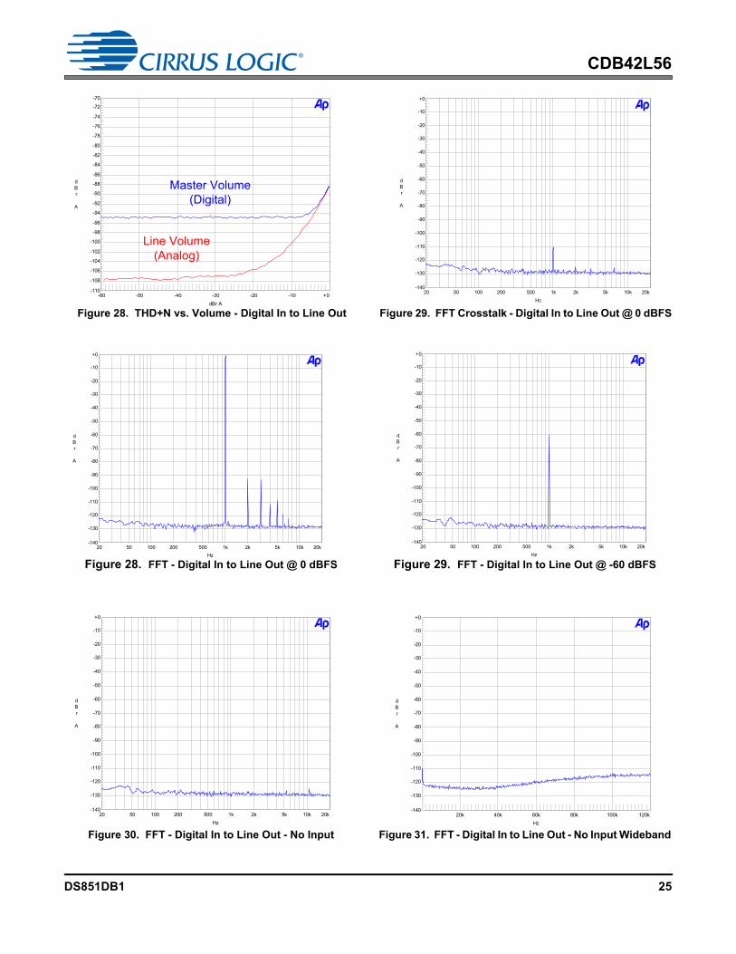
Test conditions (unless otherwise specified): TA = 25°C; VA=VCP=VLDO=VL=1.8 V; input test signal is a full-scale997 Hz sine wave; dB values relative to full-scale output; measurement bandwidth 20 Hz to 20 kHz (un-weighted);Sample Frequency = 48 kHz; +2 dB analog gain for Line Output path; -4 dB analog gain for Headphone Output path;Headphone test load: RL = 16 ; no LPF option for Headphone Output path.
Note: The total harmonic distortion + noise (THD+N) performance of the ADC in the CS42L56 is determined bythe value of the capacitor on the FILT+ pin. Larger capacitor values yield significant improvement in THD+Nat low frequencies. Fig. 10 shows the THD+N vs. frequency performance measured with several FILT+ ca-pacitor values.
-100
-60
-98
-96
-94
-92
-90
-88
-86
-84
-82
-80
-78
-76
-74
-72
-70
-68
-66
-64
-62
dBFS
20 20k50 100 200 500 1k 2k 5k 10k
Hz
-100
-60
-98
-96
-94
-92
-90
-88
-86
-84
-82
-80
-78
-76
-74
-72
-70
-68
-66
-64
-62
dBFS
-120 -20-100 -80 -60 -40
dBr
Figure 10. THD+N vs. Freq. - Analog In to Digital Out Figure 11. THD+N vs. Amplitude - Analog In to Digital Out
2.2µF
10µF
22µF
-140
+0
-130
-120
-110
-100
-90
-80
-70
-60
-50
-40
-30
-20
-10
dBFS
20 20k50 100 200 500 1k 2k 5k 10k
Hz
-140
+0
-130
-120
-110
-100
-90
-80
-70
-60
-50
-40
-30
-20
-10
dBFS
20 20k50 100 200 500 1k 2k 5k 10k
Hz
Figure 12. FFT - Analog In to Digital Out @ -1 dBFS Figure 13. FFT - Analog In to Digital Out @ -60 dBFS
Contacting Cirrus Logic SupportFor all product questions and inquiries, contact a Cirrus Logic Sales Representative. To find the one nearest you, go to www.cirrus.com.
IMPORTANT NOTICE
Cirrus Logic, Inc. and its subsidiaries ("Cirrus") believe that the information contained in this document is accurate and reliable. However, the information is subjectto change without notice and is provided "AS IS" without warranty of any kind (express or implied). Customers are advised to obtain the latest version of relevantinformation to verify, before placing orders, that information being relied on is current and complete. All products are sold subject to the terms and conditions of salesupplied at the time of order acknowledgment, including those pertaining to warranty, indemnification, and limitation of liability. No responsibility is assumed by Cirrusfor the use of this information, including use of this information as the basis for manufacture or sale of any items, or for infringement of patents or other rights of thirdparties. This document is the property of Cirrus and by furnishing this information, Cirrus grants no license, express or implied under any patents, mask work rights,copyrights, trademarks, trade secrets or other intellectual property rights. Cirrus owns the copyrights associated with the information contained herein and givesconsent for copies to be made of the information only for use within your organization with respect to Cirrus integrated circuits or other products of Cirrus. This consentdoes not extend to other copying such as copying for general distribution, advertising or promotional purposes, or for creating any work for resale.
CERTAIN APPLICATIONS USING SEMICONDUCTOR PRODUCTS MAY INVOLVE POTENTIAL RISKS OF DEATH, PERSONAL INJURY, OR SEVEREPROPERTY OR ENVIRONMENTAL DAMAGE (“CRITICAL APPLICATIONS”). CIRRUS PRODUCTS ARE NOT DESIGNED, AUTHORIZED OR WARRANTEDFOR USE IN PRODUCTS SURGICALLY IMPLANTED INTO THE BODY, AUTOMOTIVE SAFETY OR SECURITY DEVICES, LIFE SUPPORT PRODUCTS OROTHER CRITICAL APPLICATIONS. INCLUSION OF CIRRUS PRODUCTS IN SUCH APPLICATIONS IS UNDERSTOOD TO BE FULLY AT THE CUSTOMER’SRISK AND CIRRUS DISCLAIMS AND MAKES NO WARRANTY, EXPRESS, STATUTORY OR IMPLIED, INCLUDING THE IMPLIED WARRANTIES OFMERCHANTABILITY AND FITNESS FOR PARTICULAR PURPOSE, WITH REGARD TO ANY CIRRUS PRODUCT THAT IS USED IN SUCH A MANNER. IF THECUSTOMER OR CUSTOMER’S CUSTOMER USES OR PERMITS THE USE OF CIRRUS PRODUCTS IN CRITICAL APPLICATIONS, CUSTOMER AGREES, BYSUCH USE, TO FULLY INDEMNIFY CIRRUS, ITS OFFICERS, DIRECTORS, EMPLOYEES, DISTRIBUTORS AND OTHER AGENTS FROM ANY AND ALLLIABILITY, INCLUDING ATTORNEYS’ FEES AND COSTS, THAT MAY RESULT FROM OR ARISE IN CONNECTION WITH THESE USES.
Cirrus Logic, Cirrus, and the Cirrus Logic logo designs are trademarks of Cirrus Logic, Inc. All other brand and product names in this document may be trademarksor service marks of their respective owners.
Microsoft and Windows are registered trademarks of Microsoft Corporation.