CDMA Cellular Phone Jammer EE413 – Communication Electronics Instructor: Pao-Lo Liu TA: Saurav K. Bandyopadhyay Michael D. Kaprow Justin R. Antes Adam J. Pace JAM TECH ® • Version 2005 • All Rights Reserved
Transcript
CDMA Cellular Phone Jammer
EE413 – Communication Electronics Instructor: Pao-Lo Liu TA: Saurav K. Bandyopadhyay
Michael D. KaprowJustin R. AntesAdam J. Pace
JAM TECH ® • Version 2005 • All Rights Reserved
Presentation Outline
• Goals of Project • Description and Analysis of Circuit• Demonstration of Circuit• Accomplishments• Questions
EE 413 Communication Electronics
Spring 05’
JAM TECH ® • Version 2005 • All Rights Reserve
Project Goals• To create a device that will disrupt cellular
communication with respect to the following:- Operate in the 1900 MHz band.- Disallow any communication of phones that
use that band. (Denial of Service)- Have a two meter effective blocking radius.
JAM TECH ® • Version 2005 • All Rights Reserved
EE 413 Communication Electronics
Spring 05’
Circuit Description
JAM TECH ® • Version 2005 • All Rights Reserve
EE 413 Communication Electronics
Spring 05’
TL074 Quad Op Amp
EE 413 Communication Electronics
Spring 05’
JAM TECH ® • Version 2005 • All Rights Reserve
Square Wave GeneratorGenerates the signal that will be manipulated to control the VCO.
EE 413 Communication Electronics
Spring 05’
JAM TECH ® • Version 2005 • All Rights Reserve
Integrator-The Integrator takes the square wave and transforms it into triangular wave.
- This triangular wave is what allows the VCO to sweep the band of CDMA frequencies.
EE 413 Communication Electronics
Spring 05’
JAM TECH ® • Version 2005 • All Rights Reserve
BufferBuffer prevents the noise from interfering with the Square wave generator and Integrator.
EE 413 Communication Electronics
Spring 05’
JAM TECH ® • Version 2005 • All Rights Reserve
Noise Generator-Operate a Zener diode in reverse bias to create noise.
-Amplified with 2N3904 transistor and the LM386 audio amplifier
EE 413 Communication Electronics
Spring 05’
JAM TECH ® • Version 2005 • All Rights Reserve
-Noisy signal is what overloads the frequencies.
Mixer-The mixer is where the triangular wave and the nose get mixed.
-The tuning circuit adjusts amplitude of wave and amount of noise being coupled to signal.
EE 413 Communication Electronics
Spring 05’
JAM TECH ® • Version 2005 • All Rights Reserve
Voltage Controlled Oscillator(VCO)
- An oscillator designed so the output frequency can be changed by applying a voltage to its control port or tuning port
- Crystek CVCO55BE- 1650-2050
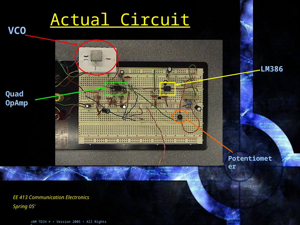
Actual Circuit
EE 413 Communication Electronics
Spring 05’
JAM TECH ® • Version 2005 • All Rights Reserve
VCO
Quad OpAmp
LM386
Potentiometer
Demonstration
JAM TECH ® • Version 2005 • All Rights Reserve
EE 413 Communication Electronics
Spring 05’
JAM TECH ® • Version 2005 • All Rights Reserve
Weeks 1 2 3 4 5 6 7 8 9
1.0 Research and Development
1.1 research technology
1.2 Develop circuit diagram
1.3 Select and order Componets
2.0 Construct Project
2.1 Build Circuit
2.2 Evaluate Circuit
2.3 Debug Circuit
3.0 Prototype Design + Evaluate
3.1Test Final Build
3.2 Demo
3.3 Documentation
Possible Improvements
• We can add another VCO to block the 800MHz digital roam feature on some phones. (Verizon comes standard)
• We can also add amplifiers that can boost the area that is affected.
JAM TECH ® • Version 2005 • All Rights Reserve
Accomplishments
• We were able to block communication coming into and going out from a CDMA phone operating on the 1900MHz frequency band.
• We were able to reach the 2 meter blocking radius.


![Kaprow-essays[1] (1)](https://static.documents.pub/doc/80x56/5695d5141a28ab9b02a3f2b7/kaprow-essays1-1.jpg)


