23

Outline• Recap of Resistivity Equations• Connection to Cell Geometry• Discussion of Cell Processing and Geometry• Series Resistance Effects Throughout

Series Resistance• V=IR• R= sum of terms:
– Bulk silicon resistance– Sheet Resistance of top Layer– External Load
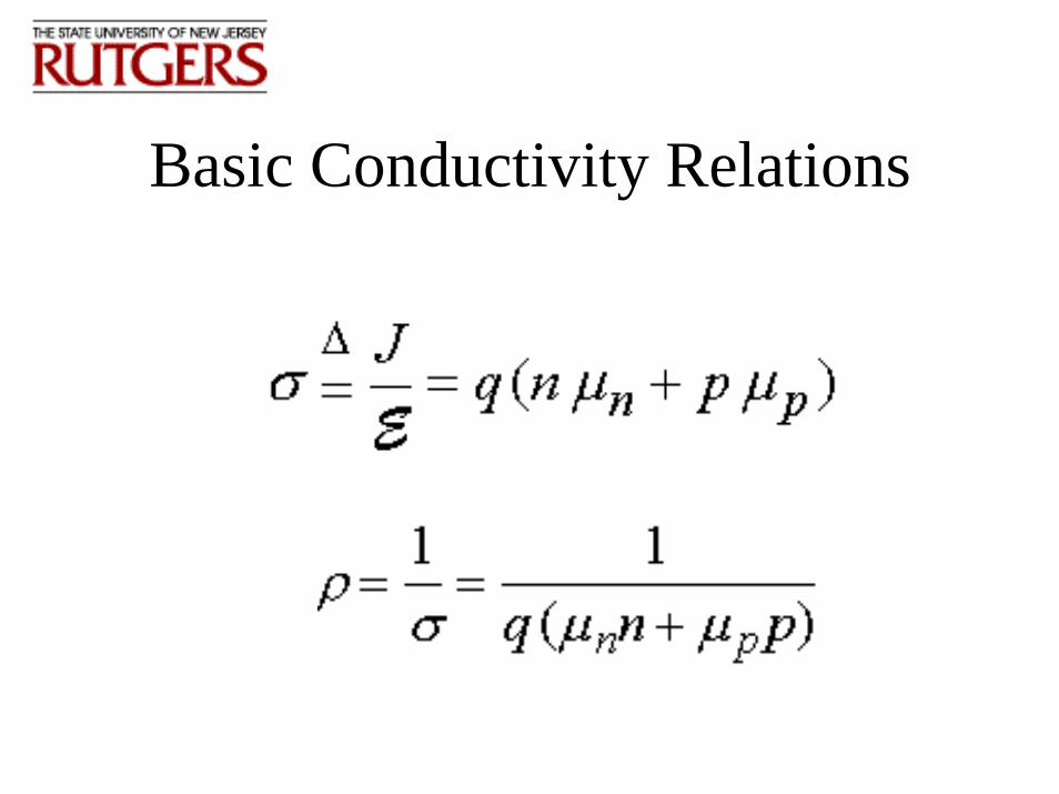
Basic Conductivity Relations

Mobility vs. Doping
Red = n-type, Blue = p-typehttp://ece-www.colorado.edu/~bart/book/mobility.htm

Resistivity vs. Doping
Red = n-type, Blue = p-typehttp://ece-www.colorado.edu/~bart/book/mobility.htm

Sheet Resistance Equations
tRS
ρ=
WLRR S=

Sheet Resistance vs. Doping
Red = n-type, Blue = p-type --- 14 mil Si wafer Thicknesshttp://ece-www.colorado.edu/~bart/book/mobility.htm

Case Study on Single Crystal Cell Processing Sequence
• Credit to SJSU/Prof. David Parent• Processing Sequence• Data

Fabrication of Solar Cells
• Diffuse donor region• Apply aluminum coating to front of wafer• Photolithography to define solar cell pattern• Etch aluminum to create solar cell pattern• Apply anti-reflection coating *• Apply aluminum coating to back of wafer • Anneal wafers• Remove outer edges of wafers

Diffuse Donor Region• Spin on phosphorous doped silica glass
Apply 3ml to front of waferSpin @ 3000 rpm for 20 seconds
• Diffuse in furnaceHeat furnace to 1100ocPush in wafers ½ inch per 15 secondsDiffuse for 1 hourPull out wafers ½ inch per 15 seconds
• Makes wafer into a large diode

Apply Aluminum Coating
• Desire 2 microns thickness• Sputter on the aluminum
Accurate and preciseFast (2 microns onto 8 wafers in 15 min.)Prone to breaking down
- Or -• Evaporate on aluminum
ReliableSlow (2 microns onto 24 wafers in 3 to 4 hours)Not very precise

Photolithography• Apply 3ml photo-resist; Spin for 20s @ 5000 rpm • Soft bake for 90oc for 30 minutes• Place solar cell mask on wafer• Place both into wooden and glass holder• Expose under lamp for 2 minutes• Develop for 15 seconds

Etch Aluminum• Etch exposed al using hot sulfuric acid• Rinse with DI water• Remove remaining PR using plasma etch

Apply Anti-reflection Coating
• Apply 3ml Titaniumsilicafilm• Spin @ 3000 rpm for 20 seconds• Spreads film to thickness of 1000 angstroms

Anneal Wafers
• Anneal for 30 minutes in furnace• Creates ohmic contact between al and Si

Cleave Edges of Wafers• Need to prevent shorting along edge of wafer• Use scribe tool to score along edges of solar cell• Cleave wafer along scoring
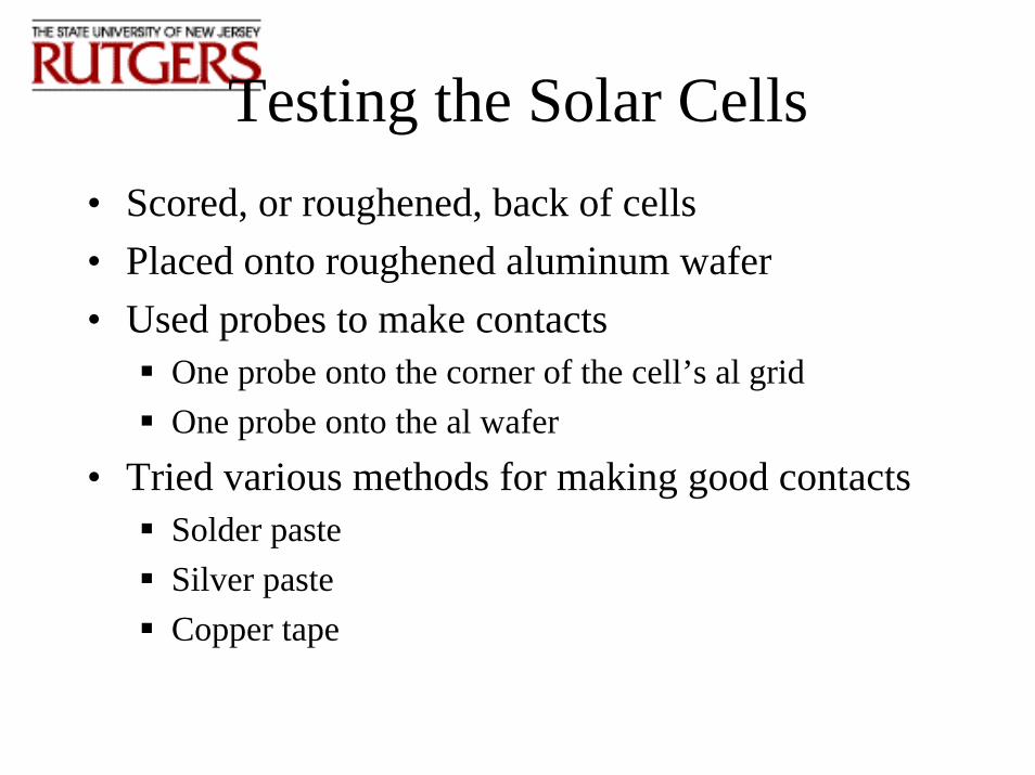
Testing the Solar Cells• Scored, or roughened, back of cells• Placed onto roughened aluminum wafer• Used probes to make contacts
One probe onto the corner of the cell’s al gridOne probe onto the al wafer
• Tried various methods for making good contactsSolder pasteSilver pasteCopper tape

Testing the Solar Cells
• Illuminated the cellUsed 75W light bulb at 3cm distance
• Connected voltmeter to probe terminalsGives open circuit voltage
• Connected current source to probe terminalsRan current against that being generated by the cellsMeasured voltage for different current levels

IV Curves for One Half of Grid Solar CellsPmax S13A = 41.9 mW Pmax S6A = 49.8
-250
-200
-150
-100
-50
0
50
-100 0 100 200 300 400 500 600 700
Voltage (mV)
Cur
rent
(mA
)
Cell S13A (Small Grid, no AR)Cell S6A (Small Grid, AR)

IV Curves for Small Grid Solar CellsPmax S21 = 61.4 mW Pmax S8 = 71.5 mW
-500
-400
-300
-200
-100
0
100
0 100 200 300 400 500 600 700
V o lt ag e ( mV )
Ce ll S 8 (S ma ll Grid, AR)
Ce ll S 21 (S ma ll Grid, no AR)

Metal Contact Geometry on Cells

Sheet Resistance vs. Doping
Red = n-type, Blue = p-type --- 14 mil Si wafer Thicknesshttp://ece-www.colorado.edu/~bart/book/mobility.htm


![THE EFFECT OF THERMOMECHANICAL PROCESSING ON THE ...boehlert/GROUP/publications/Superalloys2008M… · weldability, low-cycle fatigue resistance, and corrosion resistance [1-6]. Despite](https://static.documents.pub/doc/80x56/604588db4cb84c75ea011fdb/the-effect-of-thermomechanical-processing-on-the-boehlertgrouppublicationssuperalloys2008m.jpg)


