Challenges on ENEPIG Finished PCBs: Gold Ball Bonding and Pad Metal Lift Young K. Song and Vanja Bukva Teledyne DALSA Inc. Waterloo, ON, Canada Abstract As a surface finish for PCBs, Electroless Nickel/Electroless Palladium/Immersion Gold (ENEPIG) was selected over Electroless Nickel/Immersion Gold (ENIG) for CMOS image sensor applications with both surface mount technology (SMT) and gold ball bonding processes in mind based on the research available on-line. Challenges in the wire bonding process on ENEPIG with regards to bondability and other plating related issues are summarized. Gold ball bonding with 25um diameter wire was performed. Printed circuit boards (PCBs) were surface mounted prior to the wire bonding process with Pb-free solder paste with water soluble organic acid (OA) flux. The standard gold ball bonding process (ball / stitch bonds) was attempted during process development and pre-production stages, but this process was not stable enough for volume production due to variation in bondability within one batch and between PCB batches. This resulted in the standard gold ball bonding process being changed to stand-off-stitch bonding (SSB) or the ball-stitch-on-ball (BSOB) bonding process, in order to achieve gold ball bonding successfully on PCBs with an ENEPIG finish for volume production. Another area of concern was pad metal lifting (PML) experienced on some PCBs, and PCB batches, where the palladium (Pd) layer was completely separated from nickel (Ni) either during wire bonding or during sample destructive wire pull tests, indicating potential failures in the remainder of the batch. Evaluation of failed PCBs was performed using cross-section analysis, X-Ray Fluorescence (XRF), and Scanning Electron Microscopy (SEM)/Energy Dispersive x-ray Spectroscopy (EDS), which identified process issues, such as inclusions, or hyper corrosion which caused either localized or complete separation of the Pd from Ni layer. Through extensive investigation, using 8D and Kepner-Tregoe problem solving methods, solutions to the problem were discovered in the majority of cases, even though the exact root cause remained unclear due to multiple PCB manufacturing variables being changed at the same time. Introduction There are various types of surface finishes of PCBs available depending on the requirements of applications. One of the most popular surface finishes used is Electroless Nickel/Immersion Gold (ENIG) with advantages such as good wettability [1,2], relatively low cost [1,2], ability to meet small form factor with finer lines, smaller pitch, and high routing density [1,3]. However, ENIG historically exhibited black pad issues [1,2,4,5] and is incompatible with the thermosonic gold ball bonding process [1,2,6]. Electrolytic nickel and electrolytic gold provides excellent wire bonding performance, but trade-offs include high process cost, poorer solder joint reliability due to the high gold content, and worse co-planarity, which limits feature densities [6]. The Electroless Ni/Electroless Pd/Immersion Gold (ENEPIG) emerged in the late 1990’s [6]. The addition of a palladium layer between nickel and gold was expected to solve the black pad issue due to hyper corrosion of Ni during gold plating because Pd serves as a barrier preventing gold bath penetration into Ni and diffusion of Ni to the surface of gold [1,2,6,7]. Gold wire bondability has been reported to be compatible with an ENEPIG plated surface finish from multiple authors [1,2, 6] and suggestions with regards to Pd and Au plating thickness [3] and purity of Pd for gold wire bonding application can be found [8]. Based on our analysis of the research available on-line, ENEPIG was selected as a surface finish for PCBs over Electroless Nickel/Immersion Gold (ENIG) for CMOS image sensor applications with both surface mount technology (SMT) and gold ball bonding processes. However, the plating specifications suggested in the literature [3, 8] could not be sourced. Gold ball bonding was preferred over aluminum wedge bonding for our applications, mainly due to faster bonding speed which would significantly affect production throughput. Challenges in the gold ball bonding process on ENEPIG finished surface mounted PCBs are described below. In addition to wire bonding challenges, pad metal lift failures between Pd and Ni layers As originally published in the IPC APEX EXPO Proceedings.
Transcript
Challenges on ENEPIG Finished PCBs: Gold Ball Bonding and Pad Metal Lift
Young K. Song and Vanja Bukva
Teledyne DALSA Inc.
Waterloo, ON, Canada
Abstract
As a surface finish for PCBs, Electroless Nickel/Electroless Palladium/Immersion Gold (ENEPIG) was selected over
Electroless Nickel/Immersion Gold (ENIG) for CMOS image sensor applications with both surface mount technology (SMT)
and gold ball bonding processes in mind based on the research available on-line. Challenges in the wire bonding process on
ENEPIG with regards to bondability and other plating related issues are summarized.
Gold ball bonding with 25um diameter wire was performed. Printed circuit boards (PCBs) were surface mounted prior to the
wire bonding process with Pb-free solder paste with water soluble organic acid (OA) flux. The standard gold ball bonding
process (ball / stitch bonds) was attempted during process development and pre-production stages, but this process was not
stable enough for volume production due to variation in bondability within one batch and between PCB batches. This
resulted in the standard gold ball bonding process being changed to stand-off-stitch bonding (SSB) or the ball-stitch-on-ball
(BSOB) bonding process, in order to achieve gold ball bonding successfully on PCBs with an ENEPIG finish for volume
production.
Another area of concern was pad metal lifting (PML) experienced on some PCBs, and PCB batches, where the palladium
(Pd) layer was completely separated from nickel (Ni) either during wire bonding or during sample destructive wire pull tests,
indicating potential failures in the remainder of the batch. Evaluation of failed PCBs was performed using cross-section
analysis, X-Ray Fluorescence (XRF), and Scanning Electron Microscopy (SEM)/Energy Dispersive x-ray Spectroscopy
(EDS), which identified process issues, such as inclusions, or hyper corrosion which caused either localized or complete
separation of the Pd from Ni layer. Through extensive investigation, using 8D and Kepner-Tregoe problem solving methods,
solutions to the problem were discovered in the majority of cases, even though the exact root cause remained unclear due to
multiple PCB manufacturing variables being changed at the same time.
Introduction
There are various types of surface finishes of PCBs available depending on the requirements of applications. One of the most
popular surface finishes used is Electroless Nickel/Immersion Gold (ENIG) with advantages such as good wettability [1,2],
relatively low cost [1,2], ability to meet small form factor with finer lines, smaller pitch, and high routing density [1,3].
However, ENIG historically exhibited black pad issues [1,2,4,5] and is incompatible with the thermosonic gold ball bonding
process [1,2,6]. Electrolytic nickel and electrolytic gold provides excellent wire bonding performance, but trade-offs include
high process cost, poorer solder joint reliability due to the high gold content, and worse co-planarity, which limits feature
densities [6].
The Electroless Ni/Electroless Pd/Immersion Gold (ENEPIG) emerged in the late 1990’s [6]. The addition of a palladium
layer between nickel and gold was expected to solve the black pad issue due to hyper corrosion of Ni during gold plating
because Pd serves as a barrier preventing gold bath penetration into Ni and diffusion of Ni to the surface of gold [1,2,6,7].
Gold wire bondability has been reported to be compatible with an ENEPIG plated surface finish from multiple authors [1,2,
6] and suggestions with regards to Pd and Au plating thickness [3] and purity of Pd for gold wire bonding application can be
found [8].
Based on our analysis of the research available on-line, ENEPIG was selected as a surface finish for PCBs over Electroless
Nickel/Immersion Gold (ENIG) for CMOS image sensor applications with both surface mount technology (SMT) and gold
ball bonding processes. However, the plating specifications suggested in the literature [3, 8] could not be sourced. Gold ball
bonding was preferred over aluminum wedge bonding for our applications, mainly due to faster bonding speed which would
significantly affect production throughput. Challenges in the gold ball bonding process on ENEPIG finished surface
mounted PCBs are described below. In addition to wire bonding challenges, pad metal lift failures between Pd and Ni layers
As originally published in the IPC APEX EXPO Proceedings.
during wire bonding and the destructive pull test, and attempts to determine the root causes of pad metal lifts are presented.
To identity the root cause of pad metal lift, 8D and Kepner-Tregoe problem solving techniques were used.
Experimental
Printed circuit board
Printed circuit boards (PCBs) discussed in this paper are for multiple image sensor product applications with different PCB
layouts. There were 5 different bare board samples (a batch or batches) as shown in Table 1. All the PCBs utilized for gold
ball bonding process were surface mounted with water soluble organic acid (OA) flux prior to wire bonding process at the
same contract manufacturer. PCB sample E which was surface mounted with no-clean flux and was aluminum wire bonded,
will be reviewed for PML results only. The plating specifications and flux types used for PCB assembly for different bare
board samples are summarized in Table 1.The PCB material for all the products is FR4 with multiple layers with thickness of
about 1.8mm except for that from sample E which is about 1.3mm.
Table 1-SMT Process Used and Plating Specifications
Bare board
sample
Flux type Bonding Process Plating thickness specifications (um)
Ni (P) Pd (P) Au
A OA gold ball bonding 3.0-5.08 0.1-0.2 0.05-0.15
B OA gold ball bonding 3.0-8.0 0.3-1.0 0.05-0.18
C OA gold ball bonding 3.0-5.08 0.1-0.2 0.05-0.15
D OA gold ball bonding 3.0-5.08 0.1-0.2 0.05-0.15
E No clean aluminum wedge bonding 3.0-6.0 0.05-0.30 > 0.03
Wire bonding
All the PCB samples in Table 1 were sourced for production use. Some PCBs from samples A, B, and C were selected for
gold wire bonding evaluation (wire pull strength evaluation) and the results are discussed in the following gold ball bonding
section. From 5 samples, PMLs were observed from samples A, D, and E during production builds. Those samples are
discussed in the PML section.
The evolution of gold ball bonding process on ENEPIG surface finished PCBs is to be examined. Figure 1 shows a partial
view of the PCB layout used for one of the image sensor products showing surface mounted components and wire bonding
pads with wire bonding rings indicated by arrows as well as individually defined wire bonding pads. The area shown in a
rectangular shape in red is representative of 4 similar areas on the subject board and was used for standard gold bonding and
will be the subject of the subsequent evaluation.
Figure 1- Partial View of Sample PCB
Gold wire bonding evaluations were conducted on both bare and populated PCBs for experiments, but the wire bonding
process during image sensor assembly was applied to populated PCBs. Each populated board was plasma cleaned two times
during image sensor assembly process, once prior to die attach and another prior to wire bonding.
Wire bonding was conducted on a gold ball bonder at a bonding temperature of about 155-160°C on the PCB surface using
25um 4N gold wire. The bonding tool used for the wire bonding process was for off-the-shelf 80um pitch applications with
capillary tip dimensions of about 100um. Wire pull tests were conducted to measure wire bond strength.
Results and Discussions
Gold Ball Bonding
The standard gold ball bonding process makes a bonded wire that consists of a ball bond and a stitch bond as shown in Figure
2 and Figure 3, respectively. The ball bond, also called the first bond, is commonly made on die bonding pads, and the stitch
bond, also called the second bond, is made on substrate bonding pads. In Figure 2 and Figure 3, both ball bonds and stitch
bonds are made on a PCB substrate and the wire bonding evaluation is focused on stitch bond (second bond) capability on a
PCB. In general, bonding windows for the stitch bonds (second bonds) are smaller than those for the ball bonds (first bonds)
which means that stitch bonds are more susceptible to non-sticking due to plating quality or surface contamination compared
The standard gold wire bonding process as shown in Figure 2 and Figure 3 has been planned as the wire bonding process at
the beginning of process development based on the literature reviews [1,2,6]. However, it has been noticed that wire pull
strength of populated boards varies significantly within and between the batches. Figure 4 and Figure 5 show the box plots of
pull strength of populated boards compared to that of bare board samples A and B. The box plots show the median in the
central rectangle and the central rectangle shows interquartile range. In addition, bare boards baked at 245°C/5min are
included in Figure 4 to simulate the effect of temperature during the SMT process on wire pull strength. This was based on
the assumption that if a 245°C/5min bake only affects the wire bondability, Ni (or other metallic elements such as Cu)
diffusion to a wire bonding surface would be a potential mechanism for wire bonding issues for populated boards.
Wire bonds were made in PCB areas as shown in Figure 1 in red for wire pull strength comparison for the standard gold
bonding process. For comparison between bare and populated boards, boards from the same bare board batch were used to
eliminate the effect of batch to batch variation. As shown in Figure 4 and Figure 5, it is obvious that wire pull strength of
populated boards is lower than that of bare boards. However, the bare boards baked at 245°C/5min., in order to simulate
thermal effect during SMT process, do not show any degradation in wire pull strength compared to bare boards, indicating
that Ni migration is not likely to occur to wire bonding surfaces during the SMT process.
Note that all of the samples evaluated have been subjected to die attach cure at 150°C/40min. Even though boards were
washed with extra cycles using deionized (DI) water to remove OA flux residues at the subcontractor and plasma cleaned
during image sensor assembly in-house, there seemed to be some level of contamination still remaining on wire bonding pads
from the SMT process affecting wire bondability. However, contamination was not noticeable on an optical microscope
from the populated boards used in Figure 4 and Figure 5.
In addition to potential contamination during the SMT process, another potential issue observed was variation in flatness
and/or roughness of the bonding surface, which was indicated by non-uniform tool marks on the PCB pad surface. There was
one outlier with low pull strength value obtained from bare board 3 and there were three non-sticking bonds during wire
bonding from populated boards 3 in Figure 4. Low pull strength from bare board 3 and non-sticking bonds from populated
boards might be related to insufficient squash of bonding wire due to the non-flat bonding surface. Otherwise, ENEPIG
plated boards seem to show good wire bondability on the bare board level.
Figure 4 - Wire Pull Strength Comparison Between Bare and Populated Boards from Sample A
Figure 5 –Wire Pull Strength Comparison Between Bare and Populated Boards from Sample B
Figure 6 shows tool mark variation observed during evaluation, likely related to surface flatness or roughness. A tool mark
shape (Figure 6, right-bottom) exhibits the preferred full circle, but most tool mark shapes are broken circles. One low pull
strength value from bare board 3 in Figure 4 is from the bond with the tool mark at the left-top in Figure 6 (half or less than
half circle opposite to squashed wire). Very similar tool marks are also observed from the non-stuck wire bonds on
populated boards 3 in Figure 4.
Figure 6 - Variation in Tool Marks
Figure 7 shows the pull strength variation of mixed batches of populated boards from sample C as an example of potential
wire pull variation of populated boards using the standard gold ball bonding process. However, it could not be clearly
determined whether the plating process or the SMT process was responsible for the variation in pull strength for each board
used for Figure 7.
Figure 7 - Wire Pull Strength from Mixed Batches of Populated Boards from Sample C
Due to the variation and degradation of wire bondability of the standard gold bonding process on populated boards for our
image sensor applications, the wire bonding process was changed, first from the originally planned standard ball bonding
process, then to security bump process, and ultimately to the stand-off-stitch bond (SSB) process (also called the ball-stitch-
on-ball process). The security bump process and the SSB process are also types of gold ball bonding process and the
difference between standard bonding, security bump, and SSB processes is described in detail in the following paragraphs.
Figure 8 and Figure 9 show the shapes of ball bonds on the die and stitch bonds on the PCB bonding pads for the security
bump process. Compare stitch bond shapes between the standard gold bonding process in Figure 3 and the security bump
process in Figure 9. The security bump process enhances wire pull strength on the stitch bond since additional bump is
applied on the stitch bond as shown in Figure 9, but the process still requires continuous bonding capability without non-
sticking or losing the tail during the stitch bond process.
However, when the wire bondability of the populated PCBs is not adequate, the implementation of the security bump process
does not guarantee a satisfactory result in preventing non-sticking or losing tails. A stable bonding process without wire
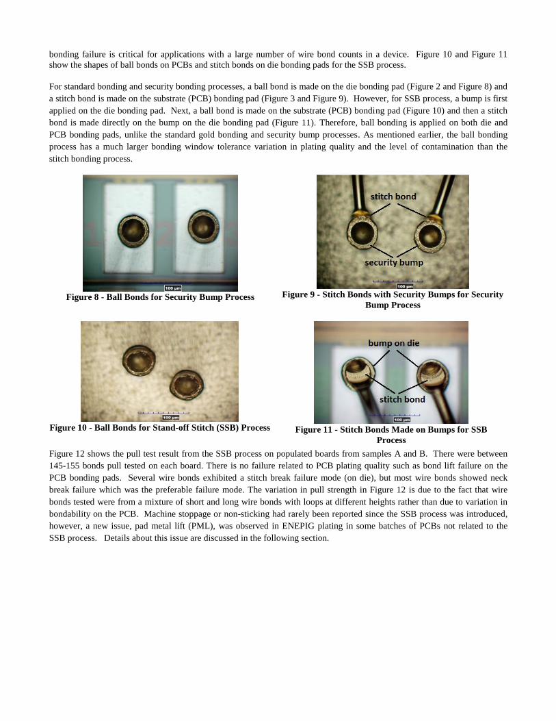
bonding failure is critical for applications with a large number of wire bond counts in a device. Figure 10 and Figure 11
show the shapes of ball bonds on PCBs and stitch bonds on die bonding pads for the SSB process. For standard bonding and security bonding processes, a ball bond is made on the die bonding pad (Figure 2 and Figure 8) and
a stitch bond is made on the substrate (PCB) bonding pad (Figure 3 and Figure 9). However, for SSB process, a bump is first
applied on the die bonding pad. Next, a ball bond is made on the substrate (PCB) bonding pad (Figure 10) and then a stitch
bond is made directly on the bump on the die bonding pad (Figure 11). Therefore, ball bonding is applied on both die and
PCB bonding pads, unlike the standard gold bonding and security bump processes. As mentioned earlier, the ball bonding
process has a much larger bonding window tolerance variation in plating quality and the level of contamination than the
stitch bonding process.
Figure 8 - Ball Bonds for Security Bump Process
Figure 9 - Stitch Bonds with Security Bumps for Security
Bump Process
Figure 10 - Ball Bonds for Stand-off Stitch (SSB) Process
Figure 11 - Stitch Bonds Made on Bumps for SSB
Process
Figure 12 shows the pull test result from the SSB process on populated boards from samples A and B. There were between
145-155 bonds pull tested on each board. There is no failure related to PCB plating quality such as bond lift failure on the
PCB bonding pads. Several wire bonds exhibited a stitch break failure mode (on die), but most wire bonds showed neck
break failure which was the preferable failure mode. The variation in pull strength in Figure 12 is due to the fact that wire
bonds tested were from a mixture of short and long wire bonds with loops at different heights rather than due to variation in
bondability on the PCB. Machine stoppage or non-sticking had rarely been reported since the SSB process was introduced,
however, a new issue, pad metal lift (PML), was observed in ENEPIG plating in some batches of PCBs not related to the
SSB process. Details about this issue are discussed in the following section.
Figure 12 - Wire Pull Strength from Populated Boards with SSB Process
Pad metal lift
Another area of concern was pad metal lift (PML) experienced on some PCBs and PCB batches where the palladium (Pd)
layer was completely separated from the nickel (Ni) either during wire bonding or during the sample destructive wire pull
tests. PMLs have been observed from both bare and populated boards, therefore, they do not seem to be related to the SMT
process. Figure 13 shows the bottom of the lifted bond as an example.
Separation of the Pd layer from the Ni layer was confirmed by EDS analyses conducted on the area on the bonding pad with
the lifted bond and the bottom of lifted bonds as shown in Figure 14 and Figure 15, respectively. Ni was the major element
in the area on the bonding pad with a lifted bond in Figure 14 and Pd was the major element detected at the bottom of the
lifted bond in Figure 15.
Figure 13 - Bottom of a Lifted Bond
Figure 14 - EDS Analysis Spectrum Obtained from The Area on Bonding Pad with Lifted Bond
Figure 15 - EDS Analysis Spectrum Obtained from The Bottom of Lifted Bond
A PML was observed on 3 different PCB samples. The following section presents the various degrees of the PML
experienced on the PCB samples.
Sample A
One of the incidents where PML was observed on the sample A of the PCBs is shown as per Figure 16 and Figure 17.
Figure 16 - Five Black Circles Represent PML Including Attempts to Repair
Figure 17 – Zoom in on PML Area
The circular shape of the pad metal lifted area is the shape of the wire bond. Using an optical microscope, it is clear that the
entire area with pad metal lift looked black in color, which was different from those identified from other samples presented
in the following sections.
A supplier noticed a process issue during the production of this batch. The root cause proposed by the supplier was an
overactive Ni bath, which can be caused by temperature or excessive copper loading, or a combination of both. In this case,
it was determined that the copper loading had been excessive over the course of several consecutive loads. ENEPIG plating
was found on the solder mask and some boards failed the tape test for poor Pd adhesion to Ni. However, the tape testing,
which was performed per IPC-TM-650, was not effective in completely screening out the PCBs affected and wire bonding
failures were observed as per Figure 16 and Figure 17.
Sample D
Figure 18 shows an example of PML occurring in one of PCB batches from the sample D. PML was observed during wire
bonding. The color of the area with the lifted bonds showed mostly a mixture of fresh Ni-like color and spots in black color
as shown in Figure 18, but some showed just fresh Ni-like color in the entire area.
Figure 18 - PML from Sample D
Boards were sent for cross-section, XRF measurements and SEM analysis. Hyper-corrosion was observed through the
analysis as shown in Figure 19. It was believed that hyper-corrosion was the cause of the PML, where Pd had separated from
the Ni layer. Hyper-corrosion is a result of hyperactivity of the immersion gold bath causing severe corrosion of the nickel,
which then creates the possibility of the Pd layer having poor adhesion. Note that the top thick layer in Figure 19 is an over-
plated nickel layer, the purpose being for sample preparation.
Figure 19 - Image of Edge Hyper Corrosion at Lens 1000x (ignore top, over-plated layer for sample preparation)
Figure 20 shows a cross-sectioned view of the edge of the bonding pad. The top thick layer is the over-plated Ni layer for the
purpose of sample preparation. Hyper corrosion of Ni beneath Pd is visible in Figure 20. Figure 21 shows hyper corrosion of
Ni in the wire bonding pad in the area with the lifted Pd layer.
Figure 20 – SEM Image of the Edge of the Pad Showing Hyper Corrosion of the Ni Beneath the Pd
Figure 21 – SEM Image of the Same Failed Site Showing Lifted Pd and Hyper Corrosion of the Ni
Comparison between batches that have been successfully wire bonded and the batch which failed at wire bonding was made
in respect to plating thickness. XRF measurements of the failed board demonstrated the thinnest Pd deposit combined with
the thickest Au deposit, both within tolerance of the IPC-4556 specification for plating thickness. The combination of thin Pd
and thick Au deposit appeared to compromise Pd bond strength possibly from the undercutting of the Ni/Pd interface due to
localized heavy hyper corrosion. In technical discussions with multiple experts, it was suggested to reduce the Au thickness
range from specified 0.05 – 0.15 um to the range of 0.03 – 0.06um, and increase Pd thickness range from the specified 0.10 –
0.20 um, to 0.15 – 0.30 um as shown in Table 2. Two trials were performed with the modified plating thickness specification,
with two different suppliers and results were encouraging. No PML was observed during wire bonding and wire pull tests.
The cross-section was performed on trial boards from both suppliers and hyper corrosion was not observed.
Table 2 – Plating Thickness for Reduced Hyper Corrosion
Thickness Original specification Modified specification to
minimize hype-corrosion
Au 0.05 – 0.15 um
(2 – 6 uin)
0.03 – 0.06 um
(1.2 – 2.4 uin)
Pd 0.10 – 0.20 um
(4 – 8 uin)
0.15 – 0.30 um
(6 – 12 uin)
Ni 3 - 5um
(118 – 200 uin)
3 – 6 um
(118 – 236 uin)*
*Increased Ni thickness to be consistent with IPC-4556, not relevant to hyper corrosion investigation.
A second PML incident involving another PCB batch occurred during wire bond and wire pull tests. Boards were sent for
cross-section, XRF measurements and SEM analysis. It was determined that the cause of Pd and Ni separation in this case
was not due to hyper corrosion. Cross-sectioned boards exhibited the separation between the Pd and the Ni without hyper
corrosion of nickel. Figure 22 shows a demarcation (separation) line which should not normally be visible.
Figure 22 - Edge of the Pad Showing Demarcation Line at 1000x Lens.
SEM analysis showed some variation in the grain size of the Ni deposit from failed boards in Figure 23. However, variation
in grain size of Ni is not expected to be responsible for PML. Figure 24 shows a small area with missing Pd layer from the
surface and the grain boundary attack on the underlying nickel indicating that the Pd layer was missing when the sample was
plated in the Au bath.
Figure 23 – SEM Image of Wire Bond Pad Showing
Variation in the Grain Size of Ni Deposit at 1000x
Figure 24 – SEM Image Showing Missing Pd at 8000X
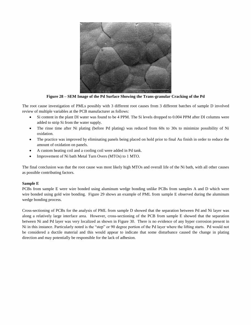
The third incident of PML was observed from a new batch of PCBs. Figure 25 shows an optical microscope image of PML
observed on this batch.
Figure 25 – Optical Microscope Image of PML
Plating thickness measurements using XRF on a same board of this batch showed inconsistency of Au and Pd thickness. The
board showed extensive hyper corrosion, causing Pd and Ni separation as shown in the cross-section of the board in Figure
26 and also showed the evidence of flaked or lifted off Pd layer at the edge of bonding pad in Figure 27. Trans-granular
cracking in the Pd layer was also observed as shown in Figure 28 even though it is not known if trans-granular cracking is
related to PML.
Figure 26 – SEM Image at 2500X Showing Extensive Hyper Corrosion
Figure 27 –SEM Image at 4000X Showing the Lifting Pd Layer
Figure 28 – SEM Image of the Pd Surface Showing the Trans-granular Cracking of the Pd
The root cause investigation of PMLs possibly with 3 different root causes from 3 different batches of sample D involved
review of multiple variables at the PCB manufacturer as follows:
Si content in the plant DI water was found to be 4 PPM. The Si levels dropped to 0.004 PPM after DI columns were
added to strip Si from the water supply.
The rinse time after Ni plating (before Pd plating) was reduced from 60s to 30s to minimize possibility of Ni
oxidation.
The practice was improved by eliminating panels being placed on hold prior to final Au finish in order to reduce the
amount of oxidation on panels.
A custom heating coil and a cooling coil were added in Pd tank.
Improvement of Ni bath Metal Turn Overs (MTOs) to 1 MTO.
The final conclusion was that the root cause was most likely high MTOs and overall life of the Ni bath, with all other causes
as possible contributing factors.
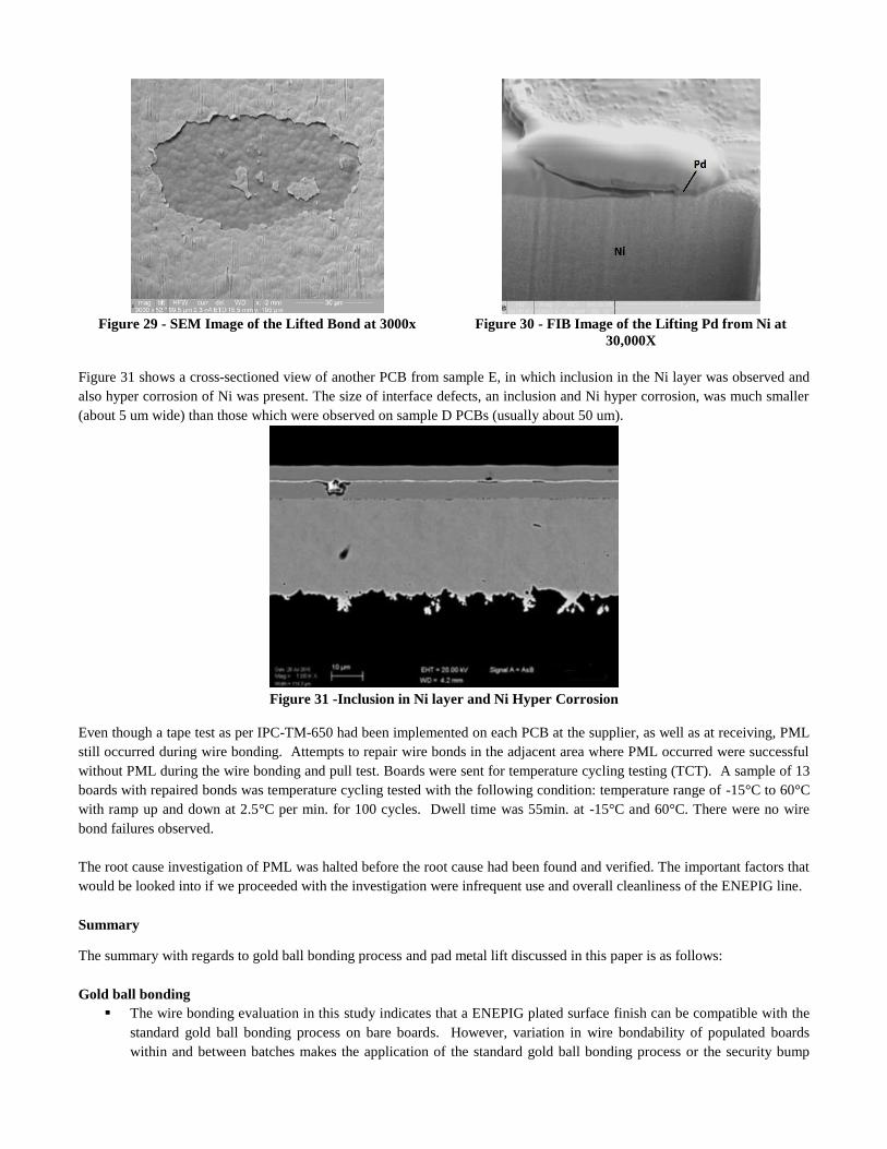
Sample E
PCBs from sample E were wire bonded using aluminum wedge bonding unlike PCBs from samples A and D which were
wire bonded using gold wire bonding. Figure 29 shows an example of PML from sample E observed during the aluminum
wedge bonding process.
Cross-sectioning of PCBs for the analysis of PML from sample D showed that the separation between Pd and Ni layer was
along a relatively large interface area. However, cross-sectioning of the PCB from sample E showed that the separation
between Ni and Pd layer was very localized as shown in Figure 30. There is no evidence of any hyper corrosion present in
Ni in this instance. Particularly noted is the “step” or 90 degree portion of the Pd layer where the lifting starts. Pd would not
be considered a ductile material and this would appear to indicate that some disturbance caused the change in plating
direction and may potentially be responsible for the lack of adhesion.
Figure 29 - SEM Image of the Lifted Bond at 3000x
Figure 30 - FIB Image of the Lifting Pd from Ni at
30,000X
Figure 31 shows a cross-sectioned view of another PCB from sample E, in which inclusion in the Ni layer was observed and
also hyper corrosion of Ni was present. The size of interface defects, an inclusion and Ni hyper corrosion, was much smaller
(about 5 um wide) than those which were observed on sample D PCBs (usually about 50 um).
Figure 31 -Inclusion in Ni layer and Ni Hyper Corrosion
Even though a tape test as per IPC-TM-650 had been implemented on each PCB at the supplier, as well as at receiving, PML
still occurred during wire bonding. Attempts to repair wire bonds in the adjacent area where PML occurred were successful
without PML during the wire bonding and pull test. Boards were sent for temperature cycling testing (TCT). A sample of 13
boards with repaired bonds was temperature cycling tested with the following condition: temperature range of -15°C to 60°C
with ramp up and down at 2.5°C per min. for 100 cycles. Dwell time was 55min. at -15°C and 60°C. There were no wire
bond failures observed.
The root cause investigation of PML was halted before the root cause had been found and verified. The important factors that
would be looked into if we proceeded with the investigation were infrequent use and overall cleanliness of the ENEPIG line.
Summary
The summary with regards to gold ball bonding process and pad metal lift discussed in this paper is as follows:
Gold ball bonding
The wire bonding evaluation in this study indicates that a ENEPIG plated surface finish can be compatible with the
standard gold ball bonding process on bare boards. However, variation in wire bondability of populated boards
within and between batches makes the application of the standard gold ball bonding process or the security bump
process difficult for volume production. Contamination on bonding pads during the SMT process seems to be the
main factor for the variation in wire bondability of populated boards.
The SSB process enables the gold ball bonding process on ENEPIG plated PCBs for volume production
applications.
Pad metal lift
PMLs were observed during the wire bonding process and/or wire pull test from multiple ENEPIG PCB samples.
An overactive Ni bath resulting in compromised Ni deposit is a potential factor in PML on wire bonding pads.
PMLs were observed with and without the evidence of hyper corrosion of Ni. PMLs due to hyper corrosion of Ni
might be related to Au and Pd thickness, and/or Ni MTOs with multiple other contributing factors.
Inclusions and hyper corrosion in the Ni layer in the wire bonding area that are at the smaller scale (approx. 5 um)
could result in reliable re-wire bonding in the same pad.
A tape test as per IPC-TM-650 is not an effective method to screen for PML on wire bonding boards.
Acknowledgments
The authors would like to acknowledge the following parties for their co-operation and technical support during PML
problem solving activities: AT&S (Leoben, Austria), FTG (Toronto, Canada), TTM (Toronto, Canada). The authors would
also like to acknowledge Gerard O’Brien from ST&S, for his ongoing support in resolution of PML and for bringing up this
issue to the IPC 4-14 Plating Processes Subcommittee.
References
[1] C. Fu, L. Hung, D. Jiang, C. Chang, Y. Wang, C. Haiso, “Evaluation of New Substrate Surface Finish: Electroless
Nickel/Electroless Palladium/Immersion Gold (ENEPIG)”, Electronic Components and Technology Conference, 1931-1935,
2008
[2] N. Sitte, “Palladium as Diffusion Barrier – a Way to Multifunctional Printed Circuit Board Finish”, Journal of the
HKPCA, Issue No. 32, 18-25, Q2, 2009
[3] Y. Oda, M. Kiso, S. Kurosaka, A. Okada, K. Kitajima, S. Hashimoto, “Study of Suitable Palladium and Gold Thickness
in ENEPIG Deposits for Lead Free Soldering and Gold Wire Bonding”, C. Uyemura and Corporation Ltd., Central Research
Laboratory, Osaka, Japan and George Milard, Don Gudeczauskas UIC Technical Center, Southinton, Connecticut, USA
[4] K. Zeng, R. Stierman, D. Abbott, and M. Murtuza, “The Root Cause of Black Pad Failure of Solder Joints with