27
Chapter 1 Fundamental Solid-State Principles

Chapter 1
Fundamental Solid-State Principles
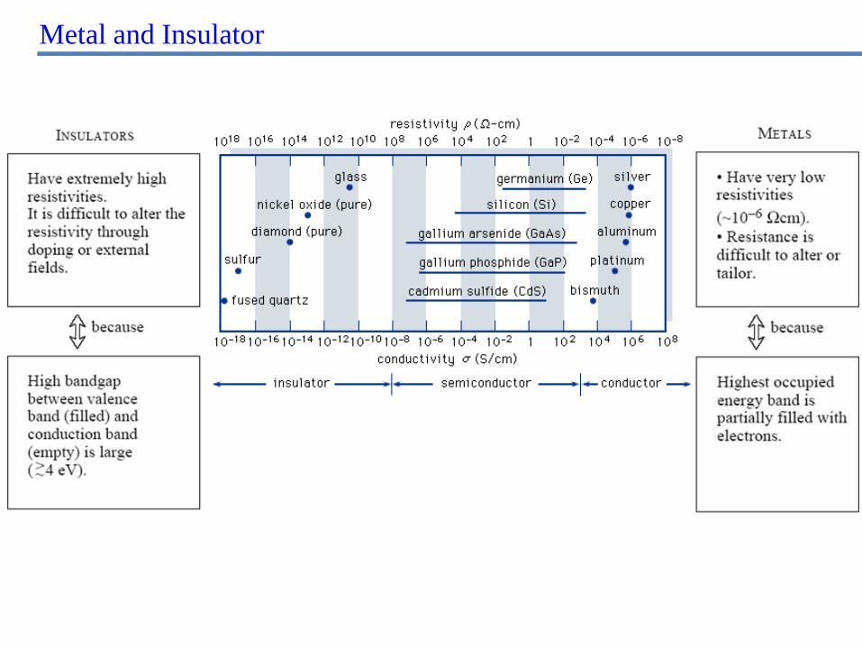
Metal and Insulator
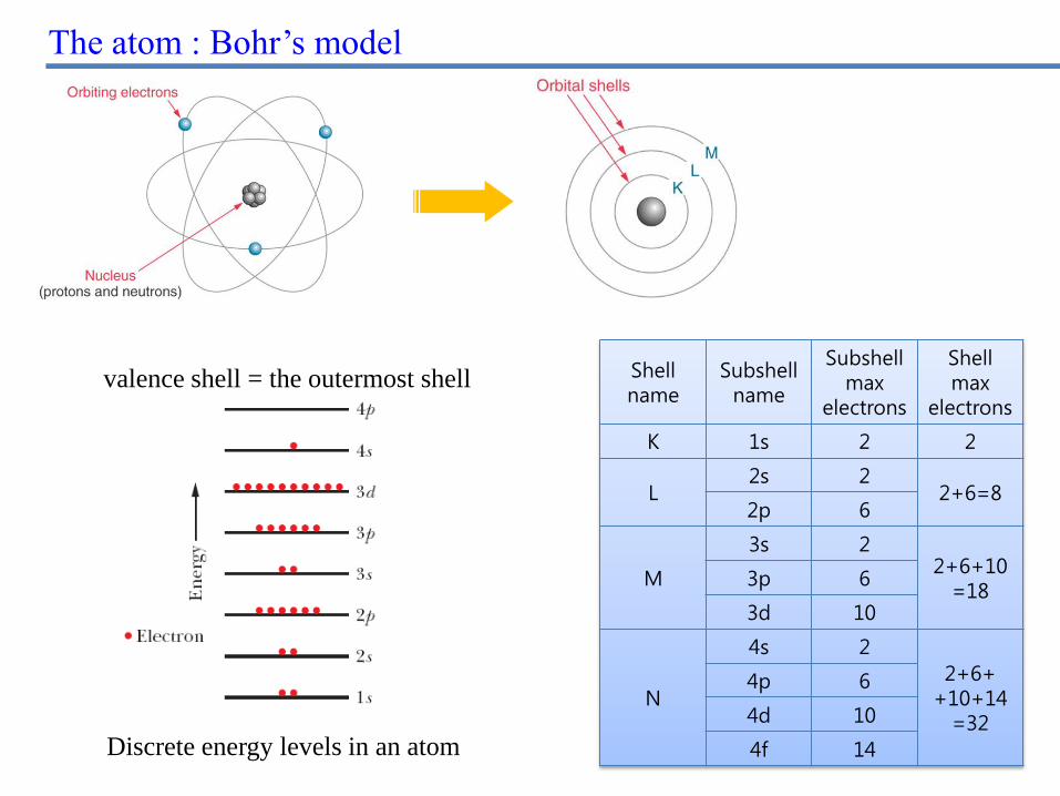
The atom : Bohr’s model
Shell name
Subshell name
Subshell max
electrons
Shell max
electrons
K 1s 2 2
L 2s 2
2+6=8 2p 6
M
3s 2 2+6+10
=18 3p 6
3d 10
N
4s 2
2+6+ +10+14
=32
4p 6
4d 10
4f 14 Discrete energy levels in an atom
valence shell = the outermost shell
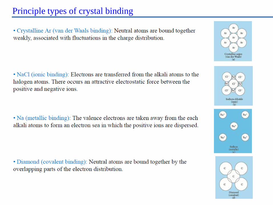
Principle types of crystal binding
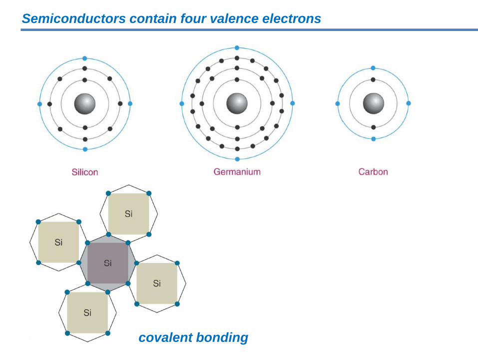
Semiconductors contain four valence electrons
covalent bonding

Probability density function for the lowest electron energy state of an isolated hydrogen atom
Overlapping two wave functions for two atoms in close proximity to each other
Interacting two electrons results in the energy level splitting into two discrete energy levels
For a regular periodic array of N hydrogen atoms, there occur N discrete energy levels
1019 atoms in 1 eV > 10-19 eV separation
E
Interatomic distance r0
Formation of energy bands
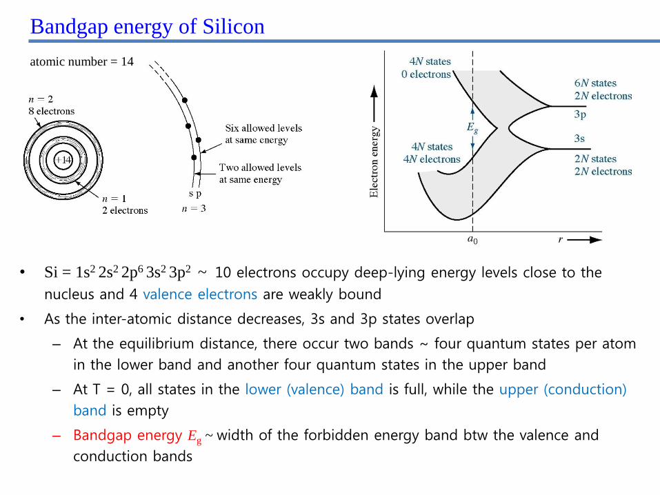
• Si = 1s2 2s2 2p6 3s2 3p2 ~ 10 electrons occupy deep-lying energy levels close to the
nucleus and 4 valence electrons are weakly bound
• As the inter-atomic distance decreases, 3s and 3p states overlap
– At the equilibrium distance, there occur two bands ~ four quantum states per atom
in the lower band and another four quantum states in the upper band
– At T = 0, all states in the lower (valence) band is full, while the upper (conduction)
band is empty
– Bandgap energy Eg ~ width of the forbidden energy band btw the valence and
conduction bands
Bandgap energy of Silicon
atomic number = 14

Electrons in crystalline solids
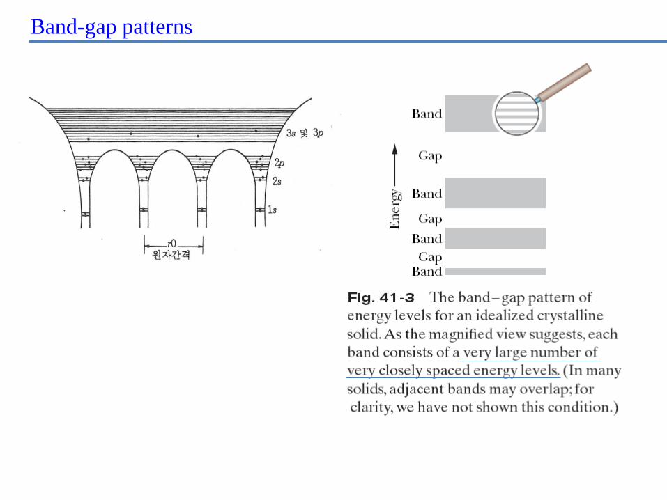
Band-gap patterns

Insulators:

Metals:
The level at the bottom of the partially filled band
of Fig. 41-5 corresponds to E =0. The highest
occupied level in this band at absolute zero (T =0 K)
is called the Fermi level, and the energy
corresponding to it is called the Fermi energy EF;
for copper, EF =7.0 eV.
The electron speed corresponding to the Fermi
energy is called the Fermi velocity vF . For copper
the Fermi speed is=1.6 x10⁶ m/s.
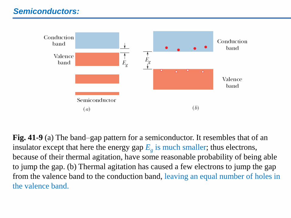
Semiconductors:
Fig. 41-9 (a) The band–gap pattern for a semiconductor. It resembles that of an
insulator except that here the energy gap Eg is much smaller; thus electrons,
because of their thermal agitation, have some reasonable probability of being able
to jump the gap. (b) Thermal agitation has caused a few electrons to jump the gap
from the valence band to the conduction band, leaving an equal number of holes in
the valence band.
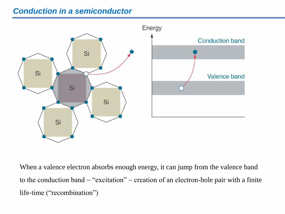
Conduction in a semiconductor
When a valence electron absorbs enough energy, it can jump from the valence band
to the conduction band ~ “excitation” ~ creation of an electron-hole pair with a finite
life-time (“recombination”)
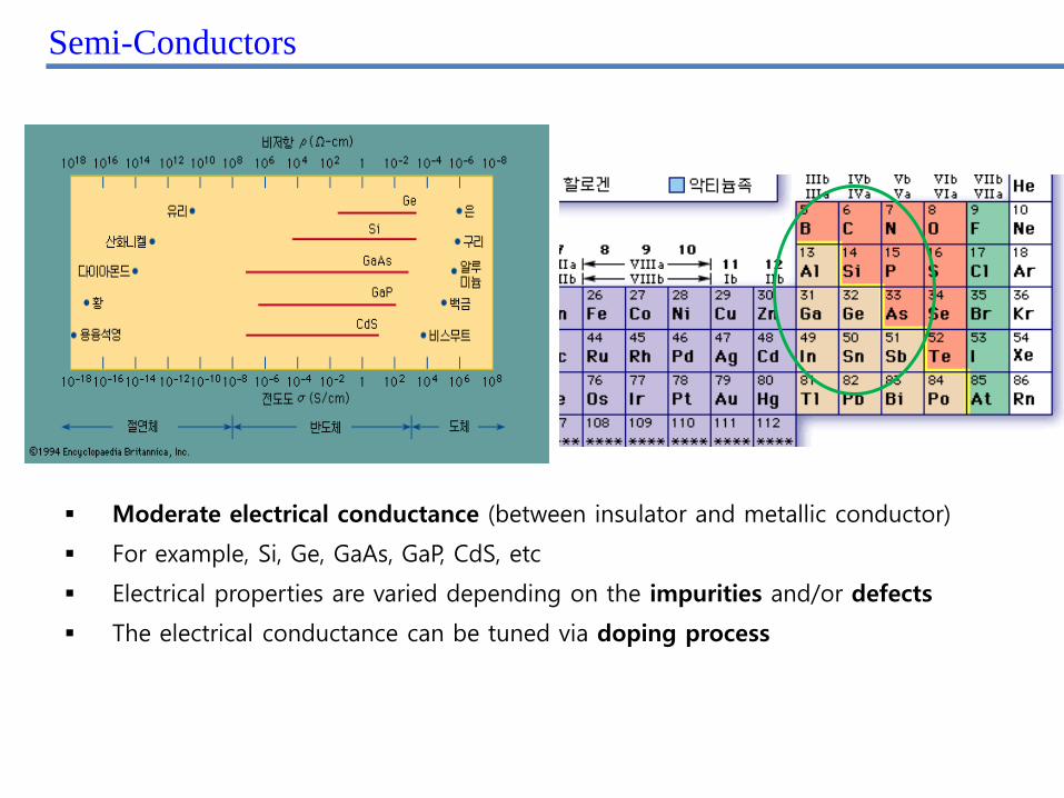
Moderate electrical conductance (between insulator and metallic conductor)
For example, Si, Ge, GaAs, GaP, CdS, etc
Electrical properties are varied depending on the impurities and/or defects
The electrical conductance can be tuned via doping process
Semi-Conductors
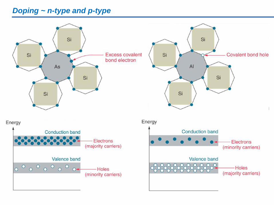
Doping ~ n-type and p-type

Doped Semiconductors:
Semiconductors
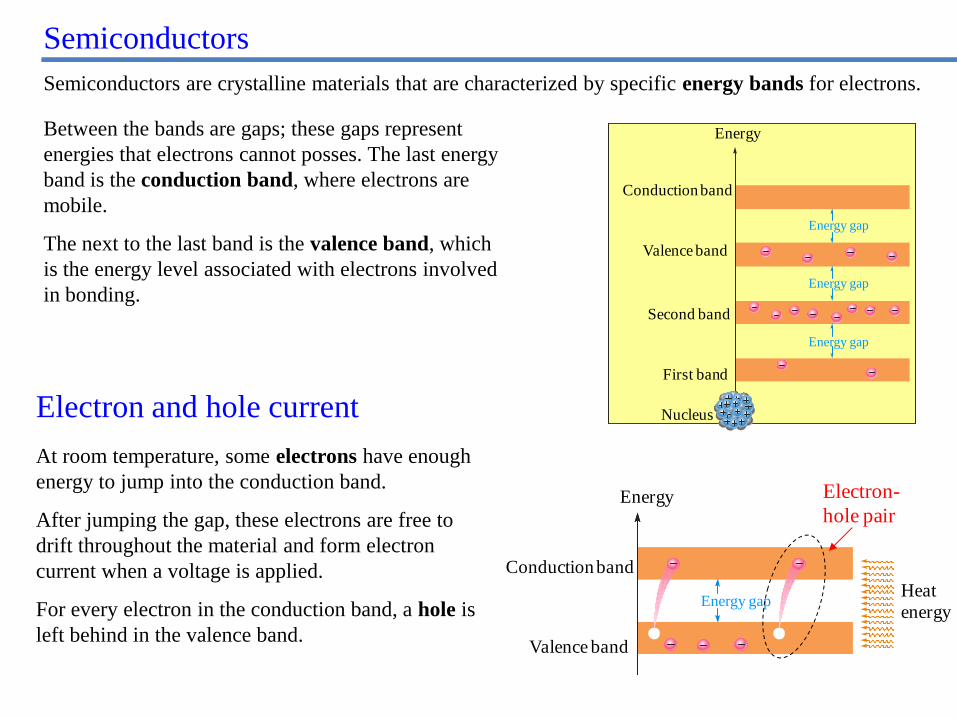
Semiconductors are crystalline materials that are characterized by specific energy bands for electrons.
Between the bands are gaps; these gaps represent
energies that electrons cannot posses. The last energy
band is the conduction band, where electrons are
mobile.
The next to the last band is the valence band, which
is the energy level associated with electrons involved
in bonding.
Nucleus
First band
Second band
Valence band
Conduction band
Energy gap
Energy gap
Energy gap
Energy
Electron and hole current
At room temperature, some electrons have enough
energy to jump into the conduction band.
After jumping the gap, these electrons are free to
drift throughout the material and form electron
current when a voltage is applied.
For every electron in the conduction band, a hole is
left behind in the valence band. Valence band
Conduction band
Energy gap
Energy
Heat
energy
Electron-
hole pair
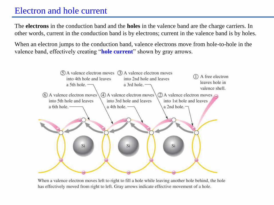
Electron and hole current
The electrons in the conduction band and the holes in the valence band are the charge carriers. In
other words, current in the conduction band is by electrons; current in the valence band is by holes.
When an electron jumps to the conduction band, valence electrons move from hole-to-hole in the
valence band, effectively creating “hole current” shown by gray arrows.
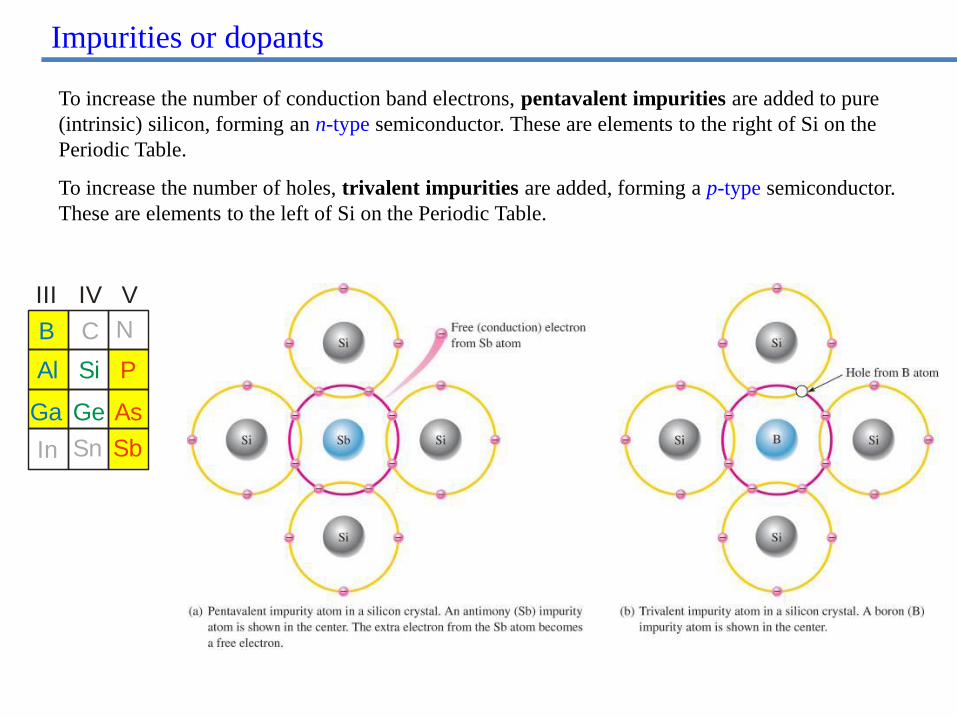
Impurities or dopants
To increase the number of conduction band electrons, pentavalent impurities are added to pure
(intrinsic) silicon, forming an n-type semiconductor. These are elements to the right of Si on the
Periodic Table.
To increase the number of holes, trivalent impurities are added, forming a p-type semiconductor.
These are elements to the left of Si on the Periodic Table.
Si
B
Al
Ga
P
As
Sb
Ge
C
Sn
N
III IV V
In

The pn junction diode
The pn junction is basically a diode, which is a device that allows
current in only one direction. A few typical diodes are shown.
When a pn junction is formed, electrons in the n-material diffuse across
the junction and recombine with holes in the p-material.
This action continues until the voltage of the barrier repels further
diffusion. Further diffusion across the barrier requires the application of
a voltage.

~ built-in potential
Barrier potential and dynamic resistance
equivalent for a diode
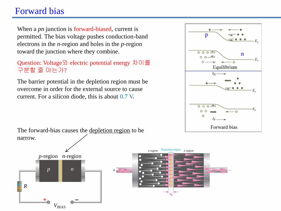
Forward bias
When a pn junction is forward-biased, current is
permitted. The bias voltage pushes conduction-band
electrons in the n-region and holes in the p-region
toward the junction where they combine.
Question: Voltage와 electric potential energy 차이를
구분할 줄 아는가?
The barrier potential in the depletion region must be
overcome in order for the external source to cause
current. For a silicon diode, this is about 0.7 V.
The forward-bias causes the depletion region to be
narrow.
p-region n-region
p n
+ -
R
VBIAS
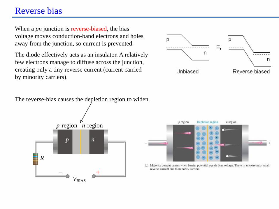
Reverse bias
When a pn junction is reverse-biased, the bias
voltage moves conduction-band electrons and holes
away from the junction, so current is prevented.
The diode effectively acts as an insulator. A relatively
few electrons manage to diffuse across the junction,
creating only a tiny reverse current (current carried
by minority carriers).
The reverse-bias causes the depletion region to widen.
p-region n-region
p n
+-VBIAS
R
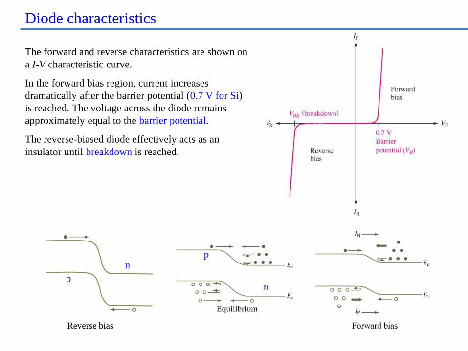
Diode characteristics
The forward and reverse characteristics are shown on
a I-V characteristic curve.
In the forward bias region, current increases
dramatically after the barrier potential (0.7 V for Si)
is reached. The voltage across the diode remains
approximately equal to the barrier potential.
The reverse-biased diode effectively acts as an
insulator until breakdown is reached.
p
n
Reverse bias

Diode structure, schematic symbol, and bias circuits.
VBIAS is the bias voltage, and VB is the barrier potential.
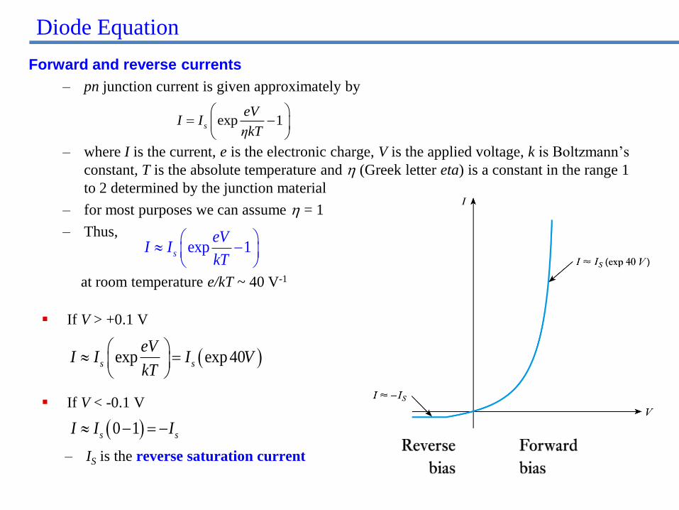
Diode Equation
Forward and reverse currents
– pn junction current is given approximately by
– where I is the current, e is the electronic charge, V is the applied voltage, k is Boltzmann’s
constant, T is the absolute temperature and (Greek letter eta) is a constant in the range 1
to 2 determined by the junction material
– for most purposes we can assume = 1
– Thus,
exp 1s
eVI I
ηkT
-
exp 1s
eVI I
kT
-
at room temperature e/kT ~ 40 V-1
If V > +0.1 V
exp exp40s s
eVI I I V
kT
If V < -0.1 V
0 1s sI I I - -
– IS is the reverse saturation current


