in DEPARTMENT OF PHYICS MOTHER TERESA SR. SEC. CO-ED SCHOOL BHOPAL MOTHER TERESA SR. SEC. CO-ED SCHOOL KOLAR ROAD BHOAPL DEPARTMENT OF PHYSICS PROJECT REPORT INVESTIGATORY PROJECT ON PN JUNCTION AND DIODES PROJECT REPORT Submitted by Govind Patel Submitted to Mrs Ratna Hajela RegisterationNo:
Transcript
in
DEPARTMENT OF PHYICS
MOTHER TERESA SR. SEC. CO-ED SCHOOL
BHOPAL
MOTHER TERESA SR. SEC. CO-ED SCHOOL
KOLAR ROAD BHOAPLDEPARTMENT OF PHYSICS
PROJECT REPORT
INVESTIGATORY PROJECT ON
PN JUNCTION AND
DIODES
PROJECT REPORT
Submitted by
Govind Patel
Submitted toMrs Ratna Hajela
RegisterationNo:
In the accomplishment of this project
successfully, many people have best
owned upon me their blessings and the
heart pledged support, this time I am
utilizing to thank all the people who
have been concerned with project.
Primarily I would thank god for being
able to complete this project with
success. Then I would like to thank my
principal Mr. James MJ and physics
teacher Mrs Ratna hajela, whose
valuable guidance has been the ones
that helped me patch this project and
make it full proof success her
suggestions and her instructions has
served as the major contributor towards
the completion of the project. Then I
would like to thank my parents and
friends who have helped me with their
valuable suggestions and guidance has
been helpful in various phases of the
completion of the project. Last but not
the least I would like to thank my
classmates who have helped me a lot.
ACKNOWLEDGEMENT
CERTIFICATE
This is to certify that project
work titled A STUDY ON PN
JUNCTIONS AND DIODES being
submitted by Govind Patel a
student of class XII-A has
successfully completed the research
on the below mentioned project
under the guidance of Mrs Ratna
Hajela ( Subject Teacher ) during
the year 2016-17 in partial
fulfillment of physics practical
examination conducted by AISSCE
Signature of external
examiner
Signature of
physics teacher
INDEX
• PN Junction
• Diode Equation
• Zener Diodes
Semiconductor: An Introduction
• Conductors: Allow Electric
current to flow through them
• Insulators: Do not Allow Electric current to flow through them
• Semiconductors: Materials whose conductivity lies in between of Conductors and Semiconductor
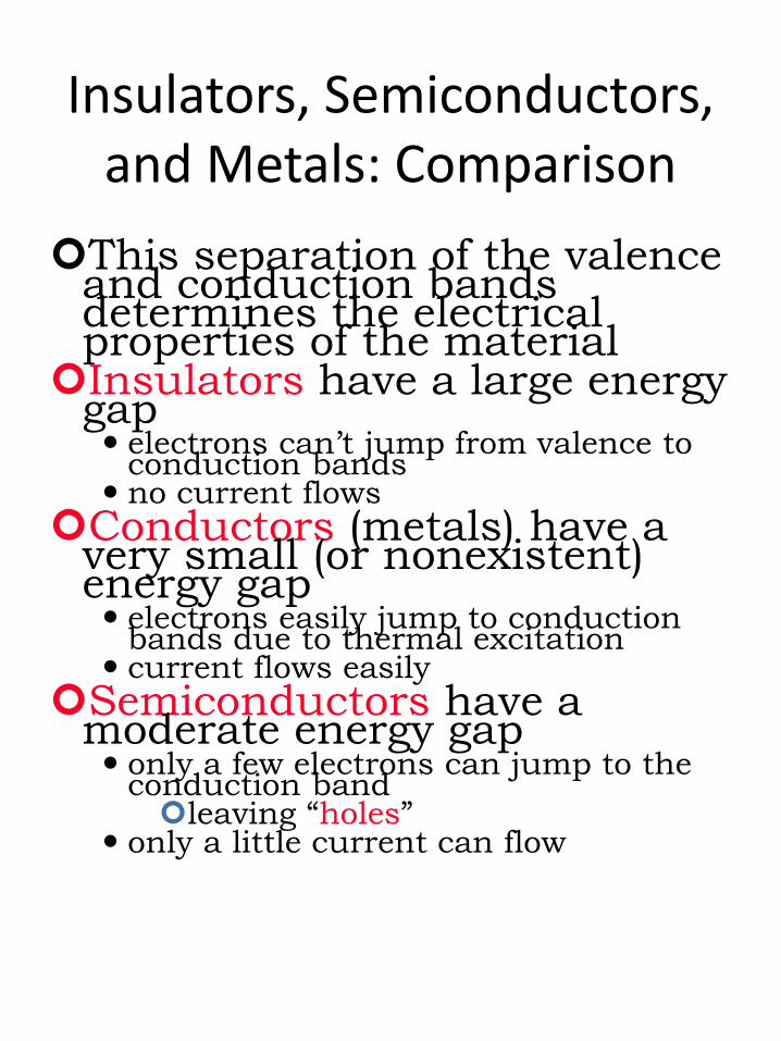
Insulators, Semiconductors,and Metals: Comparison
This separation of the valence and conduction bands determines the electrical properties of the material
Insulators have a large energy gap electrons can’t jump from valence to
conduction bands no current flows
Conductors (metals) have a very small (or nonexistent) energy gap electrons easily jump to conduction
bands due to thermal excitation current flows easily
Semiconductors have a moderate energy gap only a few electrons can jump to the
conduction bandleaving “holes”
only a little current can flow
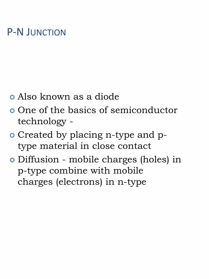
P-N JUNCTION
Also known as a diode
One of the basics of semiconductor
technology -
Created by placing n-type and p-
type material in close contact
Diffusion - mobile charges (holes) in
p-type combine with mobile
charges (electrons) in n-type
P-N JUNCTION
Region of charges left behind
(dopants fixed in crystal lattice)
Group III in p-type (one less
proton than Si- negative charge)
Group IV in n-type (one more
proton than Si - positive charge)
Region is totally depleted of mobile
charges - “depletion region”
Electric field forms due to fixed
charges in the depletion region
Depletion region has high
resistance due to lack of mobile
charges
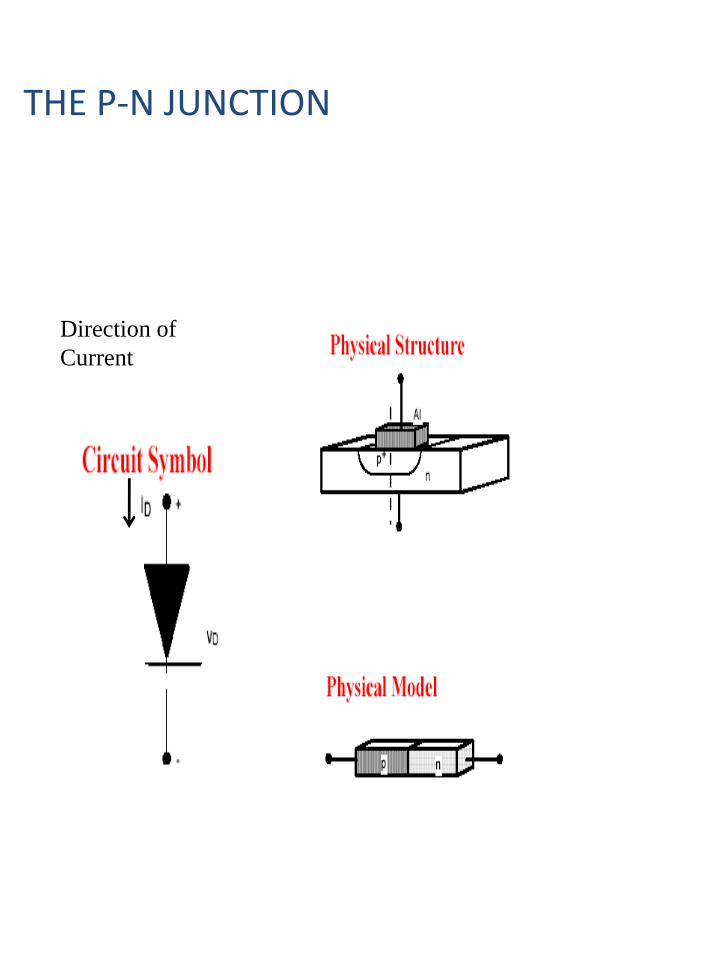
THE P-N JUNCTION
Direction of
Current
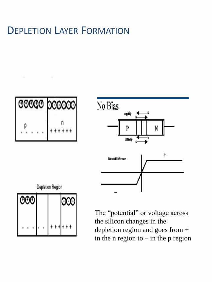
DEPLETION LAYER FORMATION
The “potential” or voltage across
the silicon changes in the
depletion region and goes from +
in the n region to – in the p region
Biasing the P-N Diode
Forward
Bias
Applies -
voltage to the
n region and
+ voltage to
the p region
CURRENT!
Reverse Bias
Applies +
voltage to n
region and –
voltage to p
region
NO
CURRENT
DIODES CAN BE
CONSIDERED AS
SWITCH
P-N Junction – Reverse Bias
positive voltage placed on n-type material
electrons in n-type move closer to positive terminal, holes in p-type move closer to negative terminal
width of depletion region increasesallowed current is essentially zero (small
“drift” current)
No current Flow
Depletion layer width
Increses
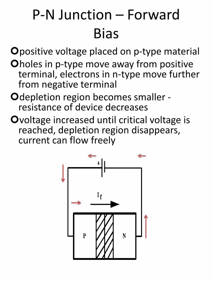
P-N Junction – Forward Bias
positive voltage placed on p-type materialholes in p-type move away from positive
terminal, electrons in n-type move further from negative terminal
depletion region becomes smaller -resistance of device decreases
voltage increased until critical voltage is reached, depletion region disappears, current can flow freely
P-N Junction - V-I characteristics
Voltage-Current relationship for a p-n junction (diode)
Current-Voltage Characteristics
THE IDEAL DIODE
Positive voltage yields
finite current
Negative voltage
yields zero currentREAL DIODE
Ideal diode equation
where:I = the net current flowing through the
diode;I0 = "dark saturation current", the diode
leakage current density in the absenceof light;V = applied voltage across the terminals
of the diode;q = absolute value of electron charge;k = Boltzmann's constant; andT = absolute temperature (K).
The diode equation gives an expression for the current through a diode as a function of voltage.