• 3 Steps to Analyze AC Circuits:1. Transform the circuit to the phasor or frequency domain.2. Solve the problem using circuit techniques (nodal analysis,
mesh analysis, superposition, etc.).3. Transform the resulting phasor to the time domain.
2
10.1 Basic Approach
• Sinusoidal Steady-State Analysis:Frequency domain analysis of AC circuit via phasors is much easier than analysis of the circuit in the time domain.
Time to Freq Solve variables in Freq
Freq to Time
PhasorLaplace xformFourier xform
PhasorInv. Laplace xform
Fourier xform
10.2 Nodal Analysis
Example: Using nodal analysis, find v1 and v2 in the figure.
3
The basic of Nodal Analysis is KCL.
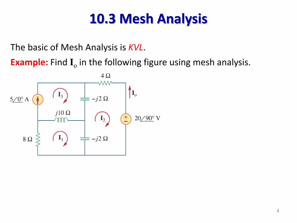
10.3 Mesh Analysis
Example: Find Io in the following figure using mesh analysis.
4
The basic of Mesh Analysis is KVL.
5
10.4 Superposition Theorem
When a circuit has sources operating at different frequencies,• The separate phasor circuit for each frequency must be solved
independently, and • The total response is the sum of time-domain responses of all
the individual phasor circuits.
6
Example: Calculate vo in the circuit using the superposition theorem.
4.3 Superposition Theorem (1)
7
- Superposition states that the voltage across (or current through) an element in a linear circuit is the algebraic sum of the voltage across (or currents through) that element due to EACH independent source acting alone.
- The principle of superposition helps us to analyze a linear circuit with more than one independent source by calculating the contribution of each independent source separately.
- Steps to Apply Superposition Principle:1. Turn off all indep. sources except one source. Find the output (v or i) due
to that active source using techniques in Chapters 2 & 3.2. Repeat Step 1 for each of the other indep. sources.3. Find total contribution by adding all contributions from indep. sources.
Note: In Step 1, this implies that we replace every voltage source by 0 V (or a short circuit), and every current source by 0 A (or an open circuit). Dependent sources are left intact because they are controlled by others.
10.5 Source Transformation (1)
8
Example: Find Io using the concept of source transformation.
9
10.5 Source Transformation (2)
4.4 Source Transformation (1)
10
- Like series-parallel combination and wye-delta transformation, source transformation is another tool for simplifying circuits.
- An equivalent circuit is one whose v-i characteristics are identicalwith the original circuit.
- A source transformation is the process of replacing a voltage source vs in series with a resistor R by a current source is in parallel with a resistor R, and vice versa.• Transformation of independent sources
• Transformation of dependent sources
The arrow of the current source is directed toward the positive terminal of the voltage source.
The source transformation is not possible when R = 0 for voltage source and R = ∞ for current source.
+ +
--+ +
- -
11
A voltage source vs connected in series with a resistor Rs and a current source is is connected in parallel with a resistor Rp are equivalent circuits provided that
& p s s s sR R v R i= =
4.4 Source Transformation (2)
10.6 Thevenin & Norton Equivalent Circuits
12
Thevenin Equivalent Norton Equivalent
Example: Find the Thevenin equivalent at terminals a–b.
4.5 Thevenin’s Theorem (1)
13
It states that a linear two-terminal circuit (Fig. a) can be replaced by an equivalent circuit (Fig. b) consisting of a voltage source VTh in series with a resistor RTh, where VTh is the open-circuit voltage at the
terminals. RTh is the input or equivalent
resistance at the terminals when the independent sources are turned off.
14
To find RTh : Case 1: If the network has no dependent sources, we turn off all
indep. Source. RTh is the input resistance of the network looking btw terminals a & b.
Case 2: If the network has depend. Sources. Depend. sources are not to be turned off because they are controlled by circuit variables. (a) Apply vo at a & b and determine the resulting io. Then RTh = vo/io. Alternatively, (b) insert io at a & b and determine vo. Again RTh = vo/io.(a) (b)
4.5 Thevenin’s Theorem (2)
15
It states that a linear two-terminal circuit (Fig. a) can be replaced by an equivalent circuit (Fig. b) consisting of a current source IN in parallel with a resistor RN,
where IN is the short-circuit current through the terminals. RN is the input or equivalent resistance at the terminals when
the indepen. sources are turned off.
(b)(a)
4.6 Norton’s Theorem (1)
10.7 Op Amp AC Circuits (1)
16
The key to analyzing op amp circuits is to keep two important properties of an ideal op amp in mind:• No current enters either of its input terminals.• The voltage across its input terminals is zero.
Example: Compute the closed-loop gain and phase shift. Assume that R1 = R2 = 10 kΩ, C1 = 2 μF , C2 = 1 μF, and ω = 200 rad/s.
Inverting Amplifier:
5.2 Ideal Op Amp
An ideal op amp has the following characteristics:1. Infinite open-loop gain, A ≈ ∞2. Infinite input resistance, Ri ≈ ∞3. Zero output resistance, Ro ≈ 0
17
Example: Determine the value of io.
when 1 Vsv =
5.3 Configurations of Op amp (1)
1 11 2
1
1
1 2
By KCL at node 1,
0 for an ideal op amp
since the noninverting terminal is grounded.
Closed-loop voltage gain is
fo i
v o i
i o
f
Rv v
R
A
v v v vi i
R R
v
v v
v
− −= ⇒ =
=
∴
=
=
= −
= −
1fR R
18
• Inverting Amplifier: reverses the polarity of the input signal while amplifying it.
Negative feedback btw the inverting input (vi) & output (vo)
vi is connected to the inverting input via R1
To find the relationship btw vi & vo:
Noninverting input is groundedEquivalent circuit
Example: Find vo & i in R1 if vi = 0.5 V, R1 = 10 kΩ, & Rf = 25 kΩ.
19
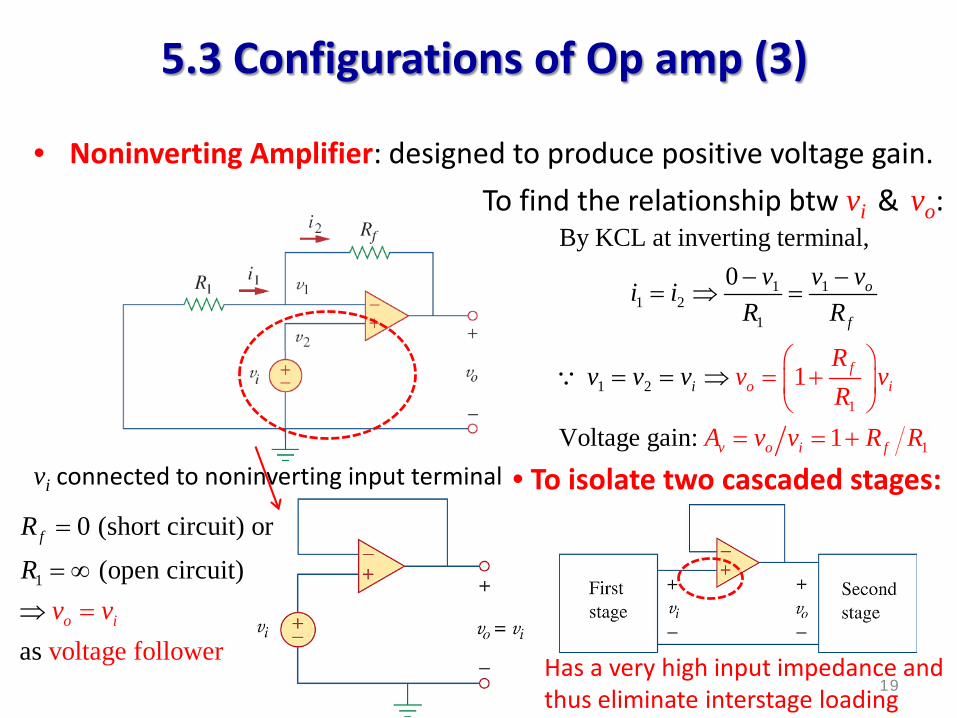
• Noninverting Amplifier: designed to produce positive voltage gain.
1 11
1
1
21
1 2
By K
1
1
CL at inverting terminal,
0
Voltage gain:
o
f
if
o i
v o i f
v v vi i
R R
Rv v v
R
A
v
v R
v
v R
− −= ⇒ =
=
= +
= = +
= ⇒
To find the relationship btw vi & vo:
vi connected to noninverting input terminal
1
0 (short circuit) or
(open c
ircuit)
a voltage follows er
f
o i
R
R
v v
=
= ∞=⇒
• To isolate two cascaded stages:
Has a very high input impedance and thus eliminate interstage loading
5.3 Configurations of Op amp (3)
10.7 Op Amp AC Circuits (2)
20
Oscillator: a circuit produces an ac waveform as output when powered by dc input.• In order for a sine wave oscillator to sustain oscillations, it must
meet the Barkhausen criteria:1. The overall gain of the oscillator must be unity or greater.
Thus losses must be compensated for by an amplifying device.
2. The overall phase shift (from the output and back to the input) must be zero.
• Three common types of sine wave oscillators are phase-shift, twin T, and Wein-bridge oscillators.
1
2of RCπ= 1.
2.
10.7 Op Amp AC Circuits (3)
21
Capacitance Multiplier: to create a large capacitance.
Example:
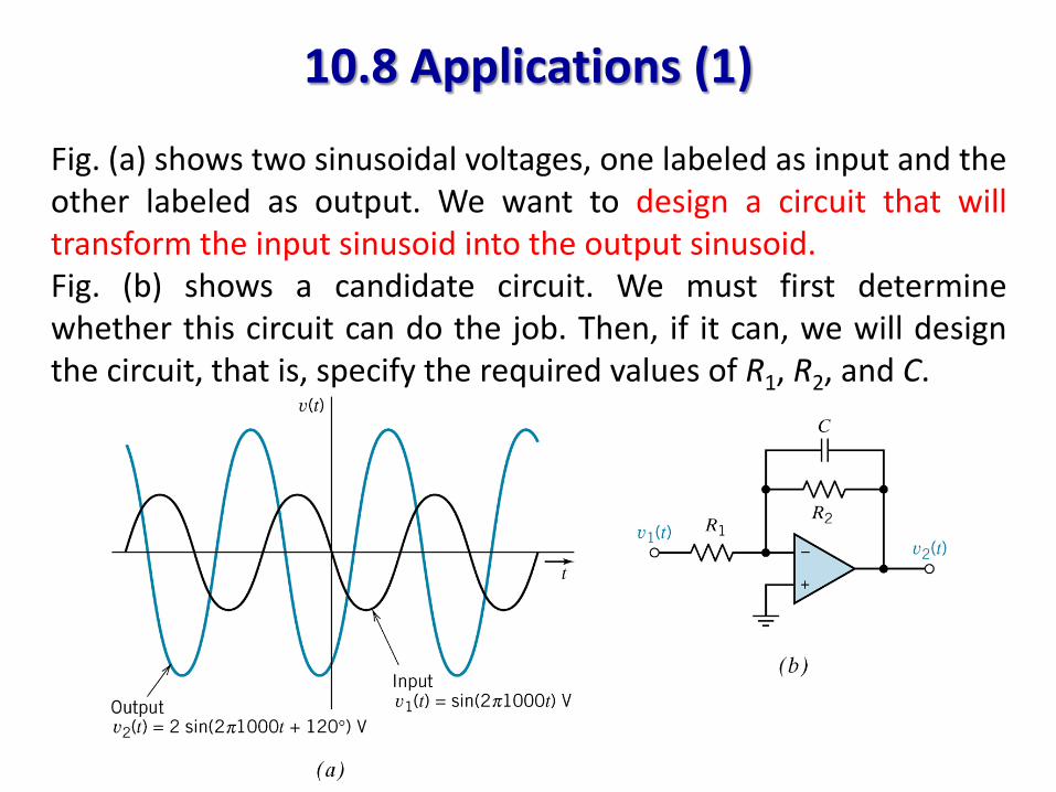
Fig. (a) shows two sinusoidal voltages, one labeled as input and theother labeled as output. We want to design a circuit that willtransform the input sinusoid into the output sinusoid.Fig. (b) shows a candidate circuit. We must first determinewhether this circuit can do the job. Then, if it can, we will designthe circuit, that is, specify the required values of R1, R2, and C.
10.8 Applications (1)
The input sinusoid is
and the corresponding phasor is
The output sinusoid is
and the corresponding phasor is
The ratio of these phasors is
The magnitude of this ratio, called the gain, G, of the circuit usedto transform the input sinusoid into the output sinusoid is
The angle of this ratio is called the phase shift, θ, of the requiredcircuit:
Therefore, we need a circuit that has a gain of 2 and a phase shiftof 120°.
1( ) sin(2 1000 ) cos(2 1000 90 ) Vv t t tπ π= = − °90
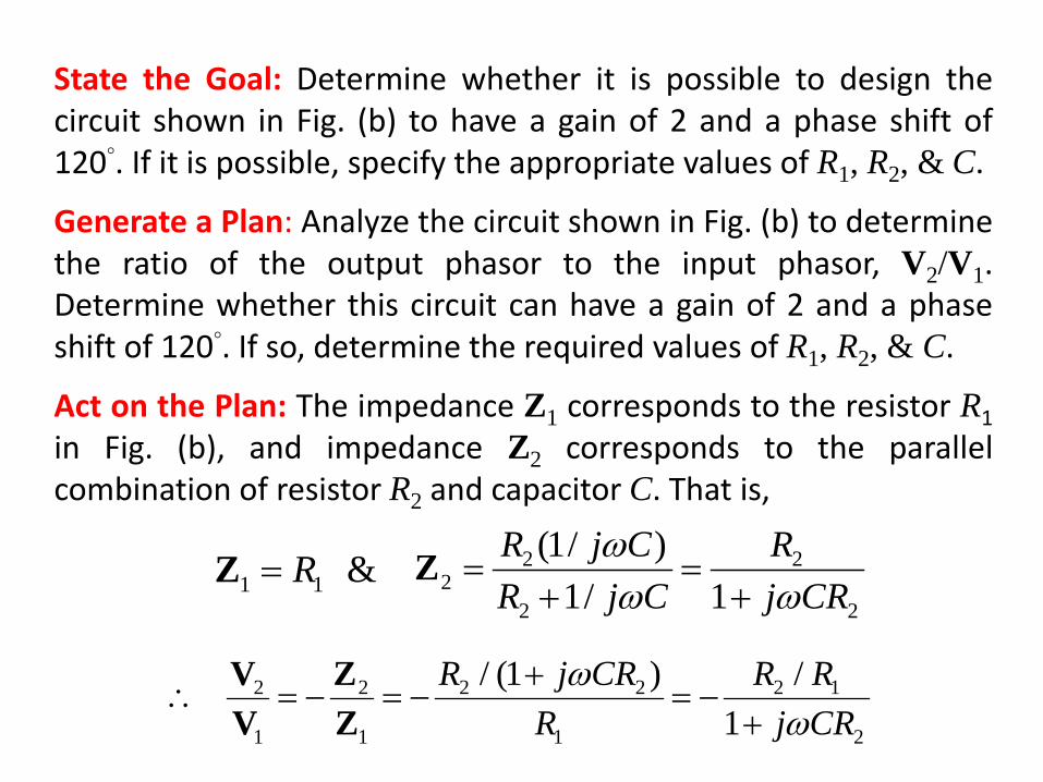
State the Goal: Determine whether it is possible to design thecircuit shown in Fig. (b) to have a gain of 2 and a phase shift of120°. If it is possible, specify the appropriate values of R1, R2, & C.
Generate a Plan: Analyze the circuit shown in Fig. (b) to determinethe ratio of the output phasor to the input phasor, V2/V1.Determine whether this circuit can have a gain of 2 and a phaseshift of 120°. If so, determine the required values of R1, R2, & C.
Act on the Plan: The impedance Z1 corresponds to the resistor R1in Fig. (b), and impedance Z2 corresponds to the parallelcombination of resistor R2 and capacitor C. That is,
1 1 &R=Z 2 22
2 2
(1/ )
1/ 1
R j C R
R j C j CR
ωω ω
= =+ +
Z
2 2 2 2 2 1
1 1 1 2
/ (1 ) /
1
R j CR R R
R j CR
ωω
+∴ = − = − = −
+V Z
V Z
The phase shift:
What values of phase shift are possible? Notice that ω, C, and R2
are all positive, which means that
Therefore, the circuit shown in Fig. (b) can be used to obtain phaseshifts between 90° and 180°. Hence, we can use this circuit toproduce a phase shift of 120°.
The gain:
To find R2
These equations can be used to design the circuit. For ω = 6283rad/s, C = 0.02 μF, G = 2, and θ = 120°, we calculate
12 2 12
1 2
/180 tan
1
R RCR
j CRθ ω
ω−= ∠ = ∠− = °−
+V
V
120 tan 90CRω−° ≤ ≤ °
2 2 1 2 1 2 1
2 2 2 21 2 2
/ / /
1 1 1 tan (180 )
R R R R R RG
j CR C Rω ω θ= = − = =
+ + + °−
V
V
2
tan(180 ) R
C
θω
°−= ⇒ 2
1 2
/
1 tan (180 )
R GR
θ=
+ °−
1 23446 and 13.78 kR R= Ω = Ω
• With the pervasive use of ac electric power in the home andindustry, it is important for engineers to analyze circuits withsinusoidal independent sources.
• The steady-state response of a linear circuit to a sinusoidal inputis itself a sinusoid having the same frequency as the input signal.
• Circuits that contain inductors and capacitors are represented bydifferential equations. When the input to the circuit is sinusoidal,the phasors and impedances can be used to represent thecircuit in the frequency domain. In the frequency domain, thecircuit is represented by algebraic equations.
• The steady-state response of a linear circuit with a sinusoidalinput is obtained as follows:1. Transform the circuit into the frequency domain, using
phasors and impedances.
10.9 Summary (1)
2. Represent the frequency-domain circuit by algebraicequation, for example, mesh or node equations.
3. Solve the algebraic equations to obtain the response of thecircuit.
4. Transform the response into the time domain, using phasors.• A circuit contains several sinusoidal sources, two cases: When all of the sinusoidal sources have the same frequency,
the response will be a sinusoid with that frequency, and theproblem can be solved in the same way that it would be ifthere was only one source.
When the sinusoidal sources have different frequencies,superposition is used to break the time-domain circuit up intoseveral circuits, each with sinusoidal inputs all at the samefrequency. Each of the separate circuits is analyzed separatelyand the responses are summed in the time domain.