130
Chapter 14 Memory System
| Date post: | 19-Dec-2015 |
| Category: |
Documents |
| View: | 236 times |
| Download: | 0 times |

Chapter 14
Memory System
HCS12 Memory System
• It has three internal memory blocks:– Program memory (EPROM or flash memory)– Data memory (SRAM)– Data EEPROM
• Many HCS12 members also support external memory.
• External memory can be SRAM, EPROM, EEPROM, or flash memory.
Internal Resource Remapping (1 of 2)
• The on-chip register block, SRAM, EEPROM, and flash memory have default locations within the 64 KB standard address.
• On-chip register block, SRAM, and EEPROM can be relocated to other places.
• It is advisable to explicitly establish these resource locations during the initialization phase of program execution to protect the inadvertent modification later.
• Writes to resource remapping registers require one cycle to take effect.
• If conflict occurs when mapping resources, the register block will take precedence over other resources.
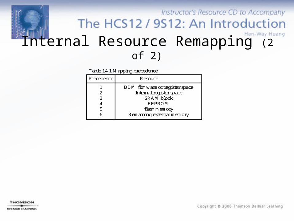
Precedence Resouce
123456
BDM firmware or register spaceInternal register space
SRAM blockEEPROM
flash memoryRemaining external memory
Table 14.1 Mapping precedence
Internal Resource Remapping (2 of 2)
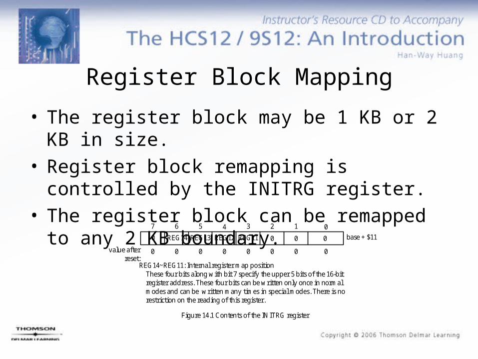
7 6 5 4 3 2 1 0
value afterreset:
0 0 0 0 0 0 0 0
0 REG14 REG13 REG12 REG11 00 0
REG14~REG11: Internal register map position These four bits along with bit 7 specify the upper 5 bits of the 16-bit register address. These four bits can be written only once in normal modes and can be written many times in special modes. There is no restriction on the reading of this register.
Figure 14.1 Contents of the INITRG register
base + $11
Register Block Mapping
• The register block may be 1 KB or 2 KB in size.• Register block remapping is controlled by the
INITRG register.• The register block can be remapped to any 2 KB
boundary.

RAM15 RAM14 RAM13 RAM12 RAM11 0 0 RAMHAL
7 6 5 4 3 2 1 0
0 0 0 0 0 01 0Value after
reset:
Figure 14.2 RAM initilization register (INITRM)
base+$10
RAM15~RAM11: Internal RAM map position These bits determine the upper five bits of the base address for the system's internal RAM array.RAMHAL: RAM high-align 0 = aligns the RAM to the lowest address ($0000) of the mappable space 1 = aligns the RAM to the highest address ($FFFF) of the mapping space.
SRAM Mapping• SRAM can be remapped to any 2 KB boundary within the 64 KB
memory space.• The SRAM remapping is controlled by the INITRM register. • RAM15 to RAM11 determine the upper five bits of the base address
for the SRAM.
7 6 5 4 3 2 1 0
value afterreset: 0 0 0 1 0 0 0 1
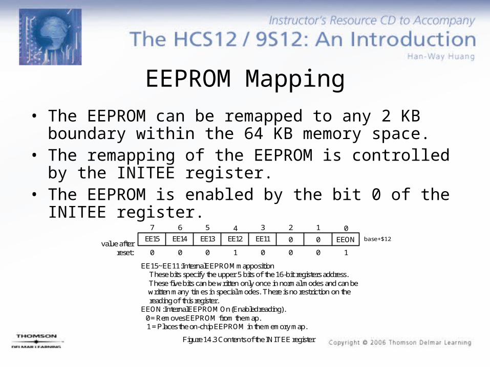
EE15 EE14 EE13 EE12 EE11 EEON0 0
EE15~EE11: Internal EEPROM map position These bits specify the upper 5 bits of the 16-bit registers address. These five bits can be written only once in normal modes and can be written many times in special modes. There is no restriction on the reading of this register.EEON: Internal EEPROM On (Enabled reading). 0 = Removes EEPROM from the map. 1 = Places the on-chip EEPROM in the memory map.
Figure 14.3 Contents of the INITEE register
base+$12
EEPROM Mapping
• The EEPROM can be remapped to any 2 KB boundary within the 64 KB memory space.
• The remapping of the EEPROM is controlled by the INITEE register.
• The EEPROM is enabled by the bit 0 of the INITEE register.
7 6 5 4 3 2 1 0
reset value:
0 0 0 0 1 1 0 _1
0 0 0 0 EXSTR1 ROMONEXSTR0 ROMHM
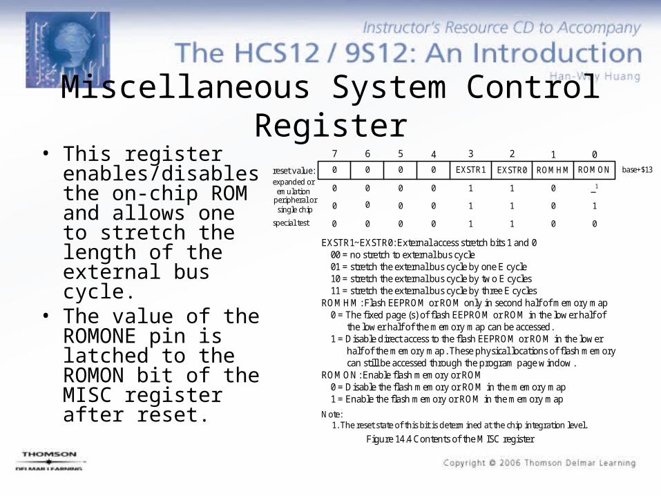
EXSTR1~EXSTR0: External access stretch bits 1 and 0 00 = no stretch to external bus cycle 01 = stretch the external bus cycle by one E cycle 10 = stretch the external bus cycle by two E cycles 11 = stretch the external bus cycle by three E cyclesROMHM: Flash EEPROM or ROM only in second half of memory map 0 = The fixed page (s) of flash EEPROM or ROM in the lower half of the lower half of the memory map can be accessed. 1 = Disable direct access to the flash EEPROM or ROM in the lower half of the memory map. These physical locations of flash memory can still be accessed through the program page window.ROMON: Enable flash memory or ROM 0 = Disable the flash memory or ROM in the memory map 1 = Enable the flash memory or ROM in the memory map
Figure 14.4 Contents of the MISC register
base+$13
expanded oremulation
peripheral orsingle chip
special test
0 0 0 0 1 1 0 1
0 0 0 0 1 1 0 0
Note: 1. The reset state of this bit is determined at the chip integration level.
Miscellaneous System Control Register• This register
enables/disables the on-chip ROM and allows one to stretch the length of the external bus cycle.
• The value of the ROMONE pin is latched to the ROMON bit of the MISC register after reset.

REG_SW0 EEP_SW1 EEP_SW0 RAM_SW2RAM_SW1RAM_SW00 0
7 6 5 4 3 2 1 0
-- -- -- -- -- -- -- --reset:
REG_SW0: Allocated system register space 0 = Allocated system register space size is 1 KB 1 = Allocated system register space size is 2 KBEEP_SW1~EEP_SW0: Allocated system EEPROM memory space 00 = 0 KB 01 = 2 KB 10 = 4 KB 11 = 8 KBRAM_SW2~RAM_SW0: Allocated system RAM memory space The allocated system RAM space size is as given in Table 14.2.
base+$1C
Figure 14.5 Memory size register zero (MEMSIZ0)
Memory Size Register Zero (MEMSIZ0)
• Read-only• This register reflects the size of the on-chip I/O
register block, EEPROM, and SRAM.

RAM_SW2:RAM_SW0Allocated
RAM spaceRAM mappable
regionINITRMbits used
RAM resetbase address(1)
Table 14.2 Allocated RAM memory space
000001010011100101110111
2K bytes4K bytes6K bytes8K bytes10K bytes12K bytes14K bytes16K bytes
2K bytes4K bytes
8K bytes(2)
8K bytes16K bytes(2)
16K bytes(2)
16K bytes(2)
16K bytes
RAM15~RAM11RAM15~RAM12RAM15~RAM13RAM15~RAM13RAM15~RAM14RAM15~RAM14RAM15~RAM14RAM15~RAM14
$0800$0000$0800$0000$1800$1000$0800$0000
Notes: 1. The RAM reset base address is based on the reset value of the INITRM register, $09. 2. Alignment of the allocated RAM space within the RAM mappable region is depedent on the value of RAMHAL.
7 6 5 4 3 2 1 0
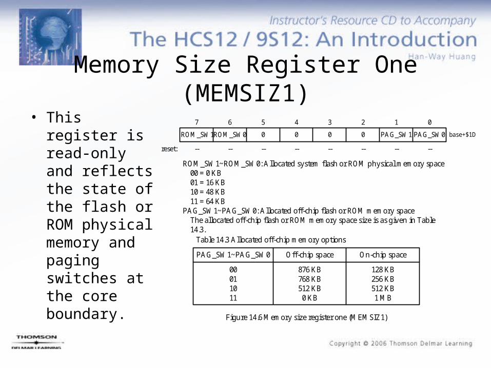
ROM_SW1ROM_SW0 0 0 0 0 PAG_SW1PAG_SW0
-- -- -- -- -- -- -- --reset:
ROM_SW1~ROM_SW0: Allocated system flash or ROM physical memory space 00 = 0 KB 01 = 16 KB 10 = 48 KB 11 = 64 KBPAG_SW1~PAG_SW0: Allocated off-chip flash or ROM memory space The allocated off-chip flash or ROM memory space size is as given in Table 14.3.
PAG_SW1~PAG_SW0 Off-chip space On-chip space
00011011
876 KB768 KB512 KB0 KB
128 KB256 KB512 KB1 MB
Table 14.3 Allocated off-chip memory options
Figure 14.6 Memory size register one (MEMSIZ1)
base+$1D
Memory Size Register One (MEMSIZ1)
• This register is read-only and reflects the state of the flash or ROM physical memory and paging switches at the core boundary.
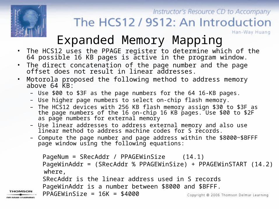
PageNum = SRecAddr / PPAGEWinSize (14.1)PageWinAddr = (SRecAddr % PPAGEWinSize) + PPAGEWinSTART (14.2)
where,SRecAddr is the linear address used in S recordsPageWinAddr is a number between $8000 and $BFFF.PPAGEWinSize = 16K = $4000
Expanded Memory Mapping• The HCS12 uses the PPAGE register to determine which of the 64 possible
16 KB pages is active in the program window. • The direct concatenation of the page number and the page offset does not
result in linear addresses. • Motorola proposed the following method to address memory above 64 KB:
– Use $00 to $3F as the page numbers for the 64 16-KB pages.– Use higher page numbers to select on-chip flash memory. – The HCS12 devices with 256 KB flash memory assign $30 to $3F as the page
numbers of the 16 on-chip 16 KB pages. Use $00 to $2F as page numbers for external memory
– Use linear addresses to address external memory and also use linear method to address machine codes for S records.
– Compute the page number and page address within the $8000~$BFFF page window using the following equations:
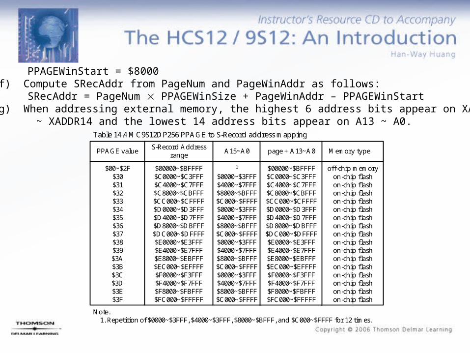
PPAGEWinStart = $8000(f) Compute SRecAddr from PageNum and PageWinAddr as follows:
SRecAddr = PageNum PPAGEWinSize + PageWinAddr – PPAGEWinStart(g) When addressing external memory, the highest 6 address bits appear on XADDR19 ~ XADDR14 and the lowest 14 address bits appear on A13 ~ A0.
Table 14.4 MC9S12DP256 PPAGE to S-Record address mapping
PPAGE valueS-Record Address
rangeA15~A0 page + A13~A0 Memory type
$00~$2F$30$31$32$33$34$35$36$37$38$39$3A$3B$3C$3D$3E$3F
$00000~$BFFFF$C0000~$C3FFF$C4000~$C7FFF$C8000~$CBFFF$CC000~$CFFFF$D0000~$D3FFF$D4000~$D7FFF$D8000~$DBFFF$DC000~$DFFFF$E0000~$E3FFF$E4000~$E7FFF$E8000~$EBFFF$EC000~$EFFFF$F0000~$F3FFF$F4000~$F7FFF$F8000~$FBFFF$FC000~$FFFFF
1
$0000~$3FFF$4000~$7FFF$8000~$BFFF$C000~$FFFF$0000~$3FFF$4000~$7FFF$8000~$BFFF$C000~$FFFF$0000~$3FFF$4000~$7FFF$8000~$BFFF$C000~$FFFF$0000~$3FFF$4000~$7FFF$8000~$BFFF$C000~$FFFF
$00000~$BFFFF$C0000~$C3FFF$C4000~$C7FFF$C8000~$CBFFF$CC000~$CFFFF$D0000~$D3FFF$D4000~$D7FFF$D8000~$DBFFF$DC000~$DFFFF$E0000~$E3FFF$E4000~$E7FFF$E8000~$EBFFF$EC000~$EFFFF$F0000~$F3FFF$F4000~$F7FFF$F8000~$FBFFF$FC000~$FFFFF
off-chip memoryon-chip flashon-chip flashon-chip flashon-chip flashon-chip flashon-chip flashon-chip flashon-chip flashon-chip flashon-chip flashon-chip flashon-chip flashon-chip flashon-chip flashon-chip flashon-chip flash
Note. 1. Repetition of $0000~$3FFF, $4000~$3FFF, $8000~$BFFF, and $C000~$FFFF for 12 times.

• Example 14.2 What are the PageNum and PageWinAddr for the SRecAddr of $E1003?• Solution: Apply equation 14.1 and 14.2 as follows:
PageNum = $E1003 / $4000 = $38PageWinAddr= ($E1003 % $4000) + $8000 = $1003 + $8000 = $9003
• Example 14.3 What is the corresponding SRecAddr for the pair of (PageNum, PageWinAddr) equal to ($20, $A003)?• Solution: Apply equation 15.3 as follows:
SRecAddr = $20 $4000 (16K) + $A003 - $8000 = $82003

On-Chip Flash Memory (1 of 3)
• The on-chip flash memory size can be 32 KB, 64 KB, 128 KB, 256KB, and 512 KB for the HCS12 devices.
• A flash memory larger than 64 KB is divided into 64-KB blocks.
• Programming and erasure of flash memory are performed by sending commands to the command register.
• The flash memory has a flexible protection scheme against accidental programming and erasure.
• The flash memory also implements security measures to prevent the application code from being pirated.
• The flash memory map is shown in Figure 14.8.

(16 bytes) flash registersregister base + $100
··register base + $10F
Flash protected low sectors0.5K, 1K, 2K, 4K bytes
flash start = $4000$4200$4400
$4800
$5000 $3E
12K
$8000
flash array
$C000
16 K pagedmemory
$38 $39 $3A $3B $3C $3D $3E $3F
Block 1 Block 0
$30 $31 $32 $33 $34 $35 $36 $37
Block 3 Block 2
flash proteected high sectors2K, 4K, 8K, 16K bytes
$FF00~$FF0F, flash protection/ security field
$3F$E000
$F000
$F800Flash end = $FFFF
Figure 14.8 MC9S12DP256 memory map
On-Chip Flash Memory (2 of 3)
On-Chip Flash Memory (3 of 3)
• The memory space from $0000 to $3FFF has been occupied by I/O registers, EEPROM, and SRAM and is not available to the flash memory.
• The first 64 KB of the flash memory is referred to as block 0 and is assigned with page numbers $3C to $3F.
• The pages with addresses from $4000 to $7FFF, $8000 to $BFFF, and $C000 to $FFFF are assigned with the page numbers of $3E, $3D, and $3F.

Flash Memory Protection (1 of 3)
• Flash memory protection is provided to prevent against accidental erasure or programming.
• Flash protection is controlled by a flash protection register (FPROT).• For HCS12 devices with multiple flash blocks, there is a separate
flash protection register for each flash block.• Flash protection registers share a common address, with the active
register selected by the bank select bits of the flash configuration register (FCNFG).
• During the HCS12 reset sequence (execution of reset start up routine), the flash protection registers for each flash block are loaded from the programmed bytes within a flash block.
• For the MC9S12DP256, the locations $FF0A,$FF0B, $FF0C, and $FF0D store the protection information of block three, two, one, and zero, respectively.

Flash Memory Protection (2 of 3)
• The contents of each FPROT register determine whether the entire block or just a subsection is protected from being accidentally erased or programmed.
• Each flash block (64 KB) can be entirely protected, or can have one or two separate protected areas.– One area to be protected is the lower protected block starting at a point
32 KB below the maximum flash block address and is extensible toward higher addresses.
– The other area is the upper protected area that ends at the top of the flash block and is extended toward lower addresses.
• The lower protected area and upper protected area do not meet up.• To change the flash protection that will be loaded on reset, the
upper sector of the flash memory must be unprotected, then the flash protect/security byte located as in Table 14.5 must be written into.
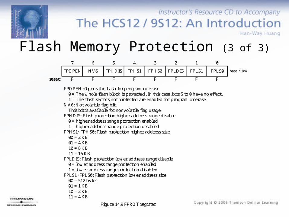
FPOPEN NV6 FPHDIS FPHS1 FPHS0 FPLDIS FPLS1 FPLS0
7 6 5 4 3 2 1 0
reset: F F F F F F F F
FPOPEN: Opens the flash for program or erase 0 = The whole flash block is protected. In this case, bits 5 to 0 have no effect. 1 = The flash sectors not protected are enabled for program or erase.NV6: Not volatile flag bit. This bit is available for nonvolatile flag usageFPHDIS: Flash protection higher address range disable 0 = higher address range protection enabled 1 = higher address range protection disabledFPHS1~FPHS0: Flash protection higher address size 00 = 2 KB 01 = 4 KB 10 = 8 KB 11 = 16 KBFPLDIS: Flash protection lower address range disable 0 = lower address range protection enabled 1 = lower address range protection disabledFPLS1~FPLS0: Flash protection lower address size 00 = 512 bytes 01 = 1 KB 10 = 2 KB 11 = 4 KB
Figure 14.9 FPROT register
base+$104
Flash Memory Protection (3 of 3)

Table 14.5 Flash protection/ options field
Address Size (bytes) Description
$FF00~$FF07$FF08~$FF09
$FF0A$FF0B$FF0C$FF0D$FF0E$FF0F
85111111
Backdoor comparison keysReservedBlock 3 flash protection byteBlock 2 flash protection byteBlock 1 flash protection byteBlock 0 flash protection byteReservedFlash options/ security byte
Flash Related Registers
• FCLKDIV• FSEC• FTSTMOD• FCNFG• FSTAT• FCMD

FDIVLD PRDIV8 FDIV5 FDIV4 FDIV3 FDIV2 FDIV1 FDIV0
7 6 5 4 3 2 1 0
reset: 0 0 0 0 0 0 0 0
FDIVLD: Clock divider loaded 0 = Register has not been written. 1 = Register has been written to since the last reset.PRDIV8: Enable prescaler by 8 0 = The input oscillator clock is directly fed into the FCLKDIV divider. 1 = Enables a divide-by-8 prescaler , to divide the flash module input oscillator clock before feeding into the CLKDIV dividerFDIV[5:0]: Clock divider bits The combination of PRDIV8 and FDIV[5:0] effectively divides the flash module input oscillator clock down to a frequency of 150KHz~200KHz. The maximum divide ratio is 512.
Figure 14.10 Flash clock divider register (FCLKDIV)
base+$100
FCLKDIV Register• The flash programming and erasure timing is
controlled by this register.• The only configuration to be done on the clock
signal is to set the prescaler to the bus clock.

KEYEN NV6 NV5 NV4 NV3 NV2 SEC1 SEC0
7 6 5 4 3 2 1 0
reset: F F F F F F F F
KEYEN: Enable backdoor key to security 0 = backdoor to flash is disabled 1 = backdoor to flash is enabledNV6~NV2: Non volatile flag bits These 5 bits are available to the user as non-volatile flagsSEC[1:0]: Memory security bits 00 = secured 01 = secured 10 = unsecured 11 = secured
Figure 14.11 Flash security register (FSEC)
base+$101
Flash Security Register (FSEC)• All the bits of this register are readable, but not writable.• This register has no reset state and must be loaded from
flash memory and, hence, its state after reset is ‘F’.• If the flash is unsecured using the backdoor key access,
the SEC bits are forced to 10.

N/ A N/ A N/ A WRALL 0 0 0 N/ A
7 6 5 4 3 2 1 0
reset: 0 0 0 0 0 0 0 0
WRALL: Write to all register banks 0 = Write only to the bank selected via BKSEL 1 = Write to all register banks
Figure 14.12 Flash test mode register (FTSTMOD)
base+$102
Flash Test Mode Register (FTSTMOD)
• This register is not banked and is mainly used to control the flash memory test modes.
• The WRALL bit allows the user to launch a command on all blocks in parallel.

CBEIE CCIE KEYACC 0 0 0 BKSEL1 BKSEL0
7 6 5 4 3 2 1 0
reset: 0 0 0 0 0 0 0 0
CBEIE: Command buffer empty interrupt enable 0 = Command buffer empty interrupts disabled 1 = An interrupt will be requested whenever the CBEIF flag is set.CCIE: Command completion interrupt enable 0 = Command complete interrupts disabled 1 = An interrupt will be requested whenever the CCIF flag is set.KEYACC: Enable security key writing 0 = Flash writes are interpreted as the start of a program or erase sequence. 1 = Writes to flash array are interpreted as keys to open the backdoor. Reads of the flash array return invalid data.BKSEL[1:0]: Register bank select 00 = flash 0 01 = flash 1 10 = flash 2 11 = flash 3
Figure 14.13 Flash configuration register (FCNFG)
base+$103
Flash Configuration Register (FCNFG)• This register enables the flash interrupts, gates the security
backdoor writes, and selects the register bank to be operated on.• For a HCS12 device with multiple flash memory banks, the BKSEL1
and BKSEL0 bits select the set of control registers to be active to be accessed.
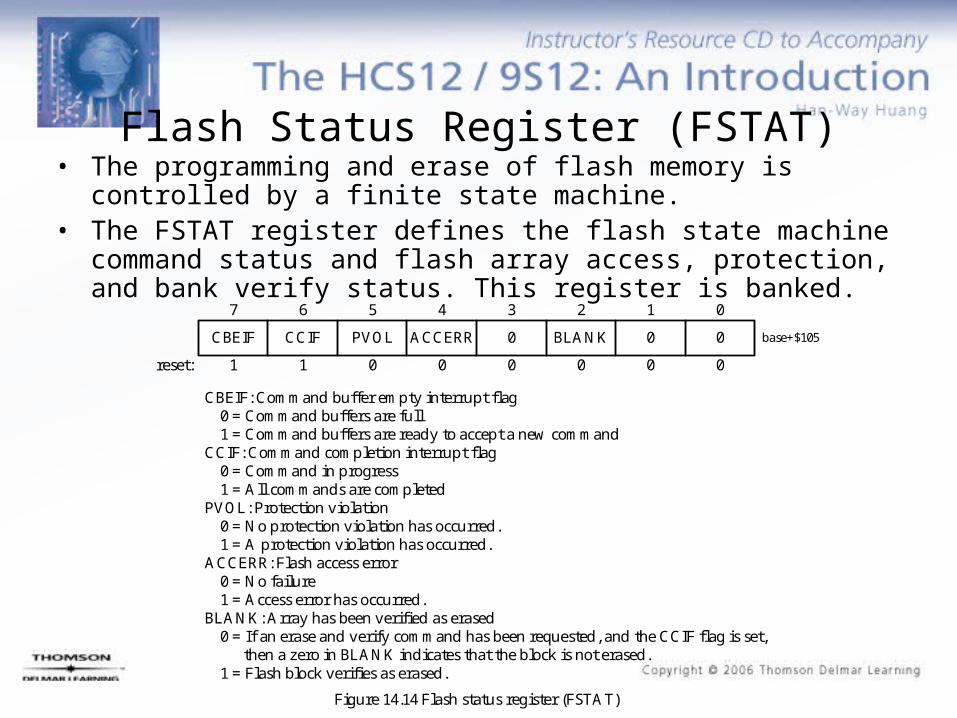
CBEIF CCIF PVOL ACCERR 0 BLANK 0 0
7 6 5 4 3 2 1 0
reset: 1 1 0 0 0 0 0 0
CBEIF: Command buffer empty interrupt flag 0 = Command buffers are full 1 = Command buffers are ready to accept a new commandCCIF: Command completion interrupt flag 0 = Command in progress 1 = All commands are completedPVOL: Protection violation 0 = No protection violation has occurred. 1 = A protection violation has occurred.ACCERR: Flash access error 0 = No failure 1 = Access error has occurred.BLANK: Array has been verified as erased 0 = If an erase and verify command has been requested, and the CCIF flag is set, then a zero in BLANK indicates that the block is not erased. 1 = Flash block verifies as erased.
Figure 14.14 Flash status register (FSTAT)
base+$105
Flash Status Register (FSTAT)• The programming and erase of flash memory is controlled by a finite
state machine.• The FSTAT register defines the flash state machine command
status and flash array access, protection, and bank verify status. This register is banked.

0 CMDB6 CMDB5 0 0 CMDB2 0 CMDB0
7 6 5 4 3 2 1 0
reset: 1 1 0 0 0 0 0 0
CMDB6, CMDB5, CMDB2, and CMDB0: Command bits Valid commands includes the following: $05 = Erase and verify $20 = Program a word (two bytes) $40 = Sector erase $41 = Bulk erase
Figure 14.15 Flash command register (FCMD)
base+$106
Flash Command Register (FCMD)
• This register defines the flash commands.• This register is banked.

Procedure to Execute the Flash Command
• Step 1– Configure the FCLKDIV register properly.
• Step 2– Make sure the sector to be erased is not protected.
• Step 3– Erase the word to be programmed and make sure it is not protected.
• Step 4– Make sure the flash address to be programmed or erased is word-
aligned.• Step 5
– If the flash address is in the range of $8000 to $BFFF, then make sure to write into the PPAGE register to select the desired page.
• Step 6– Clear the ACCERR and PVIOL bits in all flash blocks.
Secure the Flash Memory (1 of 2)
• The flash memory contents are secured by programming the security bits within the flash options/security byte at the address $FF0F.
• On devices that have a memory page window, the flash options/security byte is also available at the address $BF0F by setting the value of the PPAGE register to $3F.
• The contents of the $FF0F (or $BF0F) are copied into the flash security register (FSEC) during the reset sequence.
• The flash sector $FE00 to $FFFF must be erased before the flash options/security byte is programmed.
• Secured operation takes effect on the next reset after programming the security bits of the FSEC register to a secure value.
• The effects that the secured operation has on the HCS12 microcontroller are listed in Table 14.6.
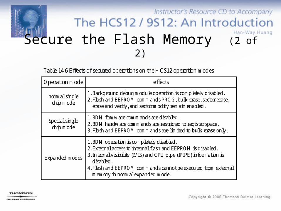
Table 14.6 Effects of secured operations on the HCS12 operation modes
Operation mode effects
normal singlechip mode
1. Background debug module operation is completely disabled.2. Flash and EEPROM commands PROG, bulk erase, sector erase, erase and verify, and sector modify remain enabled.
Special singlechip mode
1. BDM firmware commands are disabled.2. BDM hardware commands are restricted to register space.3. Flash and EEPROM commands are limited to bulk erase only.
Expanded modes
1. BDM operation is completely disabled.2. External access to internal flash and EEPROM is disabled.3. Internal visibility (IVIS) and CPU pipe (IPIPE) information is disabled.4. Flash and EEPROM commands cannot be executed from external memory in normal expanded mode.
Secure the Flash Memory (2 of 2)
Unsecuring the MCU with Backdoor Key Access
• In single chip and expanded modes, security can be temporarily disabled by means of the backdoor key access method.
• Backdoor key access requires three actions to be taken:– Program the backdoor key at $FF00~$FF07 to a valid value.– Set the KEYEN1 and KEYEN0 bits of the flash option/security byte to “10”.– In single chip mode, design applications to have the capability to write to the backdoor key
locations.• Backdoor key is not allowed to have the value of $0000 or $FFFF.• The backdoor key access sequence includes:
– Set the KEYACC bit in the flash configuration register (FCNFG).– Write the first 16-bit word of the backdoor key to $FF00.– Write the second 16-bit word of the backdoor key to $FF02.– Write the third 16-bit word of the backdoor key to $FF04.– Write the fourth 16-bit word of the backdoor key to $FF06.– Clear the KEYACC bit in the flash configuration register FCNFG.
• If all four 16-bit words match the flash contents at $FF00 to $FF07, the MCU will be forced to unsecured state “10”.

Reprogramming the Security Bits
• This method can be used only if the options/security bit is unprotected.
• In normal single chip mode, security can also be disabled by means of erasing and reprogramming the security bits within the flash option/security byte to the unsecured value.
• The erase operation will erase the entire sector from $FE00 to $FFFF, the backdoor key and interrupt vectors will also be erased.

Complete Memory Erase
• The microcontroller can be unsecured in special single chip modes by erasing the entire EEPROM and flash memory. This can be done by a BDM kit.

Configuring the FCLKDIV Register
• The FCLKDIV register controls the timing of programming and erasing of flash memory.
• It is necessary to divide the oscillator frequency down to within the 150 KHz and 200 KHz range.
• The algorithm for determining the flash clock dividing factor is illustrated in Figure 14.16.
• The following notations are used in Figure 14.16:– FCLK refers to the flash timing clock
– TBUS refers to the period of the bus clock.
– INT(x) takes integer part of x.

Start
Tbus 1 s? program/ erase impossible
PRDIV8 = 0
yes
no
oscillator clock > 12.8 MHz?
PRDCLK = oscillator clock
no
yes
PRDIV8 = 1PRDCLK = oscillator clock/ 8
PRDCLK[MHz] * (5 + Tbus[s])an integer?
FDIV[5:0]=INT(PRDCLK[MHz]*(5+Tbus[s]))
FDIV[5:0]=PRDCLK[MHz]*(5+Tbus[ms]) - 1
FCLK=PRDCLK/ (1+FDIV[5:0])
1/ FCLK[MHz] + Tbus[s] 5and FCLK 0.15MHz?
ENDyes
FDIV[5:0] 4?
Program/ erase impossible
Try to decrease Tbus
no
no
yes
Figure 14.16 PRDIV8 and FDIV bits determination procedure
no
yes
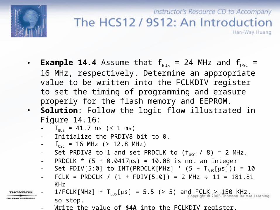
• Example 14.4 Assume that fBUS = 24 MHz and fOSC = 16 MHz, respectively. Determine an appropriate value to be written into the FCLKDIV register to set the timing of programming and erasure properly for the flash memory and EEPROM.
• Solution: Follow the logic flow illustrated in Figure 14.16: - TBUS = 41.7 ns (< 1 ms)- Initialize the PRDIV8 bit to 0.- fOSC = 16 MHz (> 12.8 MHz)- Set PRDIV8 to 1 and set PRDCLK to (fOSC / 8) = 2 MHz.- PRDCLK * (5 + 0.0417s) = 10.08 is not an integer- Set FDIV[5:0] to INT(PRDCLK[MHz] * (5 + TBUS[s])) = 10- FCLK = PRDCLK / (1 + FDIV[5:0]) = 2 MHz 11 = 181.81 KHz- 1/FCLK[MHz] + TBUS[s] = 5.5 (> 5) and FCLK > 150 KHz, so stop.- Write the value of $4A into the FCLKDIV register.

Flash Memory Programming and Erasing Algorithms
• One needs to verify that there is no pending access error or protection violation in any flash blocks. This initial set up include the following three steps:– Verify that all ACCERR and PVIOL flags in the FSTAT register
are cleared in all banks. – Write to bits BKSEL in the FCNFG register to select the bank of
registers corresponding to the flash block to be programmed or erased.
– Write to the PPAGE register to select one of the pages to be programmed if programming is to be done in the $8000~$BFFF address space.
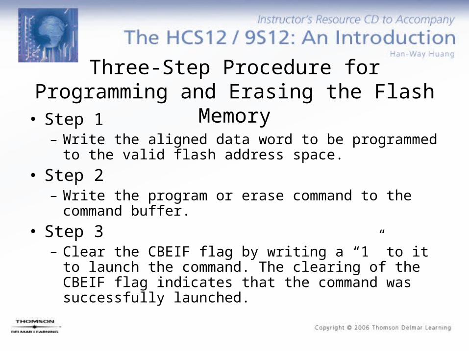
Three-Step Procedure for Programming and Erasing the Flash Memory
• Step 1– Write the aligned data word to be programmed to the
valid flash address space.
• Step 2– Write the program or erase command to the
command buffer.
• Step 3– Clear the CBEIF flag by writing a “1” to it to launch the
command. The clearing of the CBEIF flag indicates that the command was successfully launched.

• Example 14.5 Write a function to clear the ACCERR and PVIOL flags in all four blocks in the HCS12 devices with 256 KB of on-chip flash memory. • Solution:
clearflags bclr FCNFG,$03 ; select bank 0movb #ACCERR+PVIOL,FSTAT ; clear the ACCERR and PVIOL flagsbset FCNFG,$01 ; select bank 1movb #ACCERR+PVIOL,FSTAT ; clear the ACCERR and PVIOL flagsbset FCNFG,$03 ; select bank 3movb #ACCERR+PVIOL,FSTAT ; clear the ACCERR and PVIOL flagsbclr FCNFG,$01 ; select bank 2movb #ACCERR+PVIOL,FSTAT ; clear the ACCERR and PVIOL flagsrts
void clearflags (void){ FCNFG &= ~0x03; /* select bank 0 */ FSTAT = ACCERR+PVIOL; /* clear the ACCERR and PVIOL flags */ FCNFG |= 0x01; /* select bank 1 */ FSTAT = ACCERR+PVIOL; /* clear the ACCERR and PVIOL flags */ FCNFG |= 0x03; /* select bank 3 */ FSTAT = ACCERR+PVIOL; /* clear the ACCERR and PVIOL flags */ FCNFG &= 0xFE; /* select bank 2 */ FSTAT = ACCERR+PVIOL; /* clear the ACCERR and PVIOL flags */}
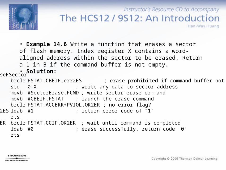
• Example 14.6 Write a function that erases a sector of flash memory. Index register X contains a word-aligned address within the sector to be erased. Return a 1 in B if the command buffer is not empty. • Solution:
EraseFSectorbrclr FSTAT,CBEIF,err2ES ; erase prohibited if command buffer not emptystd 0,X ; write any data to sector addressmovb #SectorErase,FCMD ; write sector erase commandmovb #CBEIF,FSTAT ; launch the erase commandbrclr FSTAT,ACCERR+PVIOL,OK2ER ; no error flag?
err2ES ldab #1 ; return error code of "1"rts
OK2ER brclr FSTAT,CCIF,OK2ER; wait until command is completedldab #0 ; erase successfully, return code "0"rts
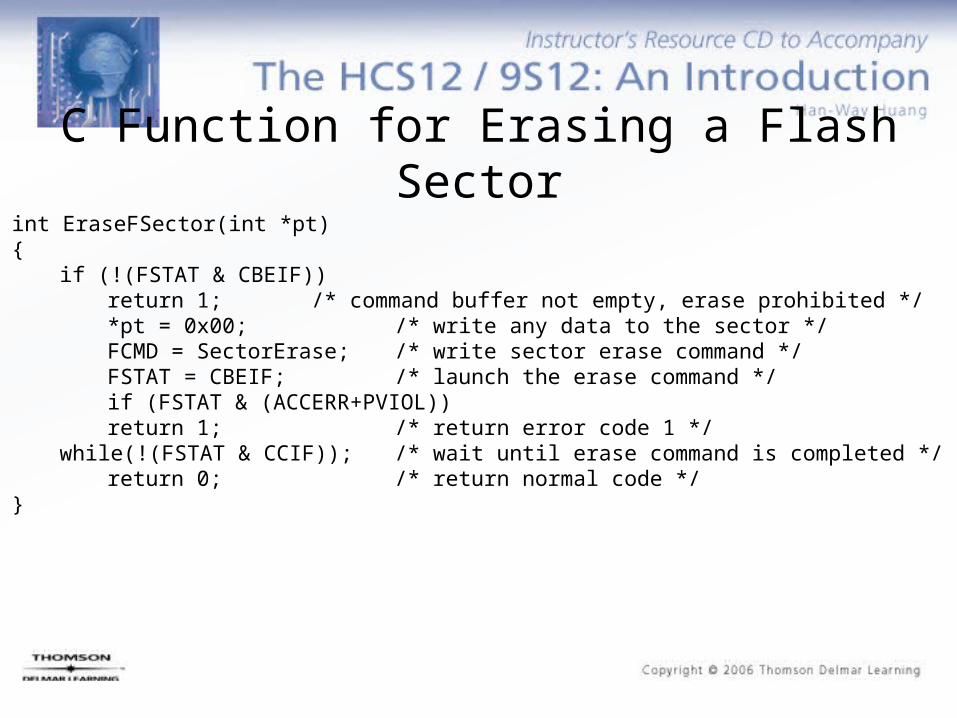
int EraseFSector(int *pt){
if (!(FSTAT & CBEIF))return 1; /* command buffer not empty, erase prohibited */
*pt = 0x00; /* write any data to the sector */ FCMD = SectorErase; /* write sector erase command */ FSTAT = CBEIF; /* launch the erase command */ if (FSTAT & (ACCERR+PVIOL)) return 1; /* return error code 1 */
while(!(FSTAT & CCIF)); /* wait until erase command is completed */ return 0; /* return normal code */}
C Function for Erasing a Flash Sector

• Example 14.7 Write a function that performs bulk erasure operation to the flash memory. The index register contains a word-aligned address of a word inside the sector to be bulk erased. Return a 1 in accumulator B if bulk erasure is not allowed.• Solution:
BulkEraseFbrset FPROT,FPOPEN+FPHDIS+FPLDIS,doBL ; Is bulk erasure allowed?ldab #1 ; return error code 1rts
doBL brclr FSTAT,CBEIF,errBL ; bulk erase prohibited if CBEIF == 0std 0,X ; write any data to sector addressmovb #BulkErase,FCMD ; write bulk erase commandmovb #CBEIF,FSTAT ; launch the erase commandbrclr FSTAT,ACCERR+PVIOL,OK2BL ; no error flag?
errBL ldab #1 ; return error code of "1"rts
OK2BL brclr FSTAT,CCIF,OK2BL ; wait until command is completedldab #0 ; erase successfully, return code "0"rts
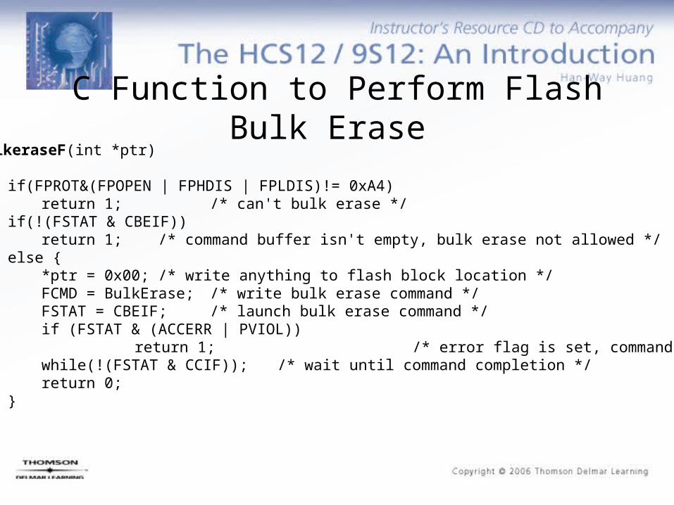
int bulkeraseF(int *ptr){ if(FPROT&(FPOPEN | FPHDIS | FPLDIS)!= 0xA4) return 1; /* can't bulk erase */ if(!(FSTAT & CBEIF)) return 1; /* command buffer isn't empty, bulk erase not allowed */ else { *ptr = 0x00; /* write anything to flash block location */ FCMD = BulkErase; /* write bulk erase command */ FSTAT = CBEIF; /* launch bulk erase command */ if (FSTAT & (ACCERR | PVIOL)) return 1; /* error flag is set, command failed */ while(!(FSTAT & CCIF)); /* wait until command completion */ return 0; }}
C Function to Perform Flash Bulk Erase
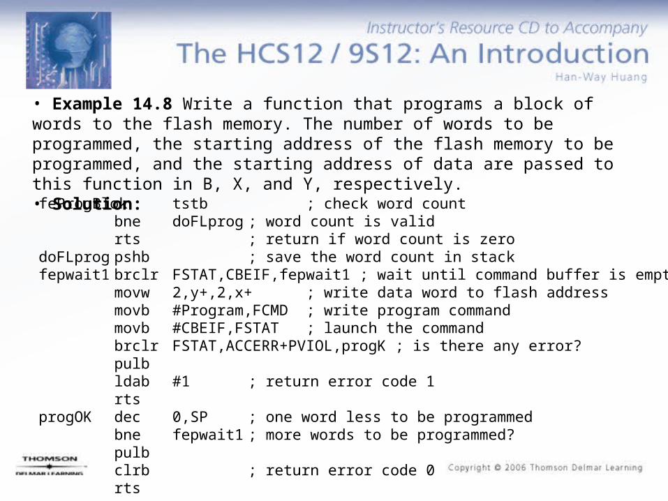
• Example 14.8 Write a function that programs a block of words to the flash memory. The number of words to be programmed, the starting address of the flash memory to be programmed, and the starting address of data are passed to this function in B, X, and Y, respectively.• Solution:
feProgBlok tstb ; check word countbne doFLprog ; word count is validrts ; return if word count is zero
doFLprog pshb ; save the word count in stackfepwait1 brclr FSTAT,CBEIF,fepwait1 ; wait until command buffer is empty
movw 2,y+,2,x+ ; write data word to flash addressmovb #Program,FCMD ; write program commandmovb #CBEIF,FSTAT ; launch the commandbrclr FSTAT,ACCERR+PVIOL,progK ; is there any error?pulbldab #1 ; return error code 1rts
progOK dec 0,SP ; one word less to be programmedbne fepwait1 ; more words to be programmed?pulbclrb ; return error code 0rts
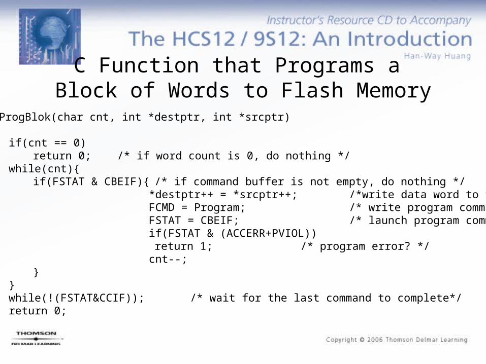
int feProgBlok(char cnt, int *destptr, int *srcptr){ if(cnt == 0) return 0; /* if word count is 0, do nothing */ while(cnt){ if(FSTAT & CBEIF){ /* if command buffer is not empty, do nothing */ *destptr++ = *srcptr++; /*write data word to flash location*/ FCMD = Program; /* write program command */ FSTAT = CBEIF; /* launch program command */ if(FSTAT & (ACCERR+PVIOL)) return 1; /* program error? */ cnt--; } } while(!(FSTAT&CCIF)); /* wait for the last command to complete*/ return 0;}
C Function that Programs a Block of Words to Flash Memory

• Example 14.9 Write a function that performs that erase-and-verify command to the flash memory. Index register contains a word-aligned address to the flash block to be erased and verified.• Solution:
feraseverify brclr FSTAT,CBEIF,cantE ; command buffer not emptystd 0,x ; write any data to flash sector addressmovb #EraseVerify,FCMD ; write the commandmovb #CBEIF,FSTAT ; launch the erase and verify commandbrclr FSTAT,ACCERR+PVIOL,EVNoErrldab #1 ; return error code 1rts
EVNoErr brclr FSTAT,CCIF,EVNoErr ; wait until command is donebrset FSTAT,BLANK,EVFOK ; successful erase and verify?
cantE ldab #1 ; flash is not blankrts
EVFOK clrb ; erase and verify OKrts

int feraseverify(int *ptr){ if(!(FSTAT & CBEIF)) return 1; /* command buffer not empty, returns */ *ptr = 0x00; /* write data to flash sector address */ FCMD = EraseVerify; /* write erase verify command */ FSTAT = CBEIF; /* launch the command */ if(FSTAT&(ACCERR | PVIOL)) return 1; /* errors have occurred */ while(!(FSTAT & CCIF)); /* wait until command is completed */ if(FSTAT & BLANK) return 0; /* command completed successfully */
elsereturn 1;
}
C Function that Performs Erase and Verify
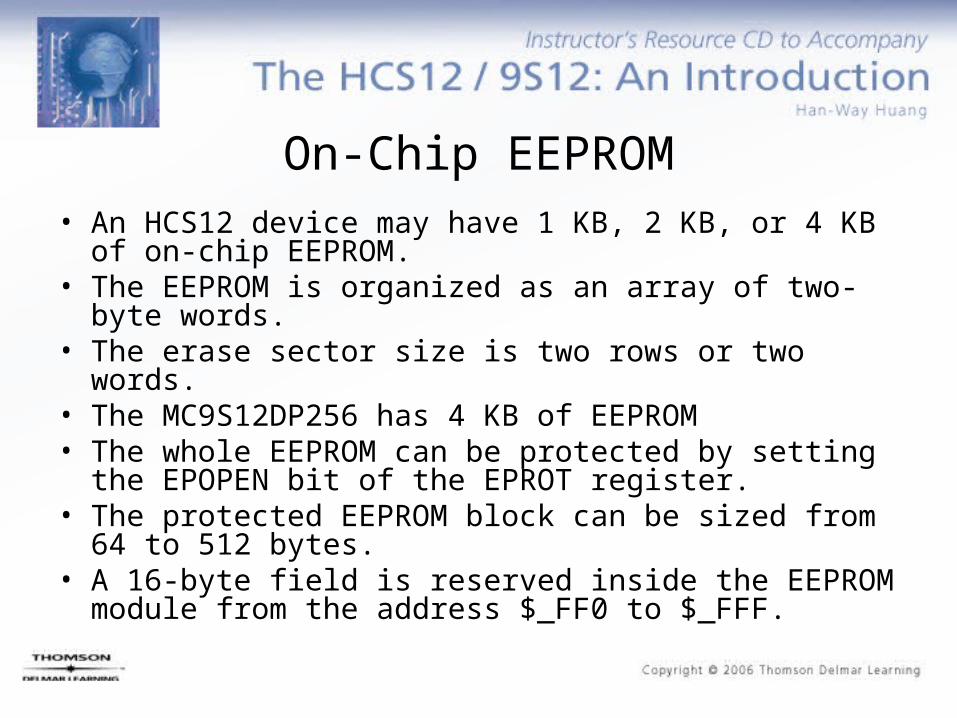
On-Chip EEPROM• An HCS12 device may have 1 KB, 2 KB, or 4 KB of on-
chip EEPROM.• The EEPROM is organized as an array of two-byte
words.• The erase sector size is two rows or two words.• The MC9S12DP256 has 4 KB of EEPROM• The whole EEPROM can be protected by setting the
EPOPEN bit of the EPROT register.• The protected EEPROM block can be sized from 64 to
512 bytes.• A 16-byte field is reserved inside the EEPROM module
from the address $_FF0 to $_FFF.
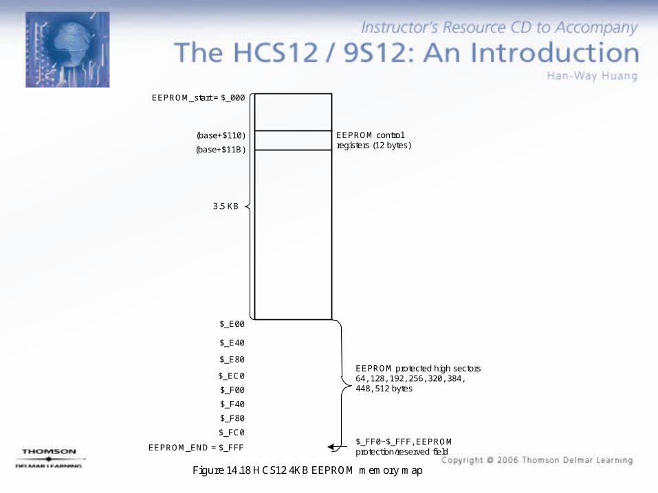
EEPROM_start = $_000
(base+$110)
(base+$11B)
EEPROM controlregisters (12 bytes)
3.5 KB
$_E00
$_E40
$_E80
$_EC0
$_F00
$_F40
$_F80
$_FC0
EEPROM_END = $_FFF
EEPROM protected high sectors64, 128, 192, 256, 320, 384,448, 512 bytes
$_FF0~$_FFF, EEPROMprotection/reserved field
Figure 14.18 HCS12 4KB EEPROM memory map
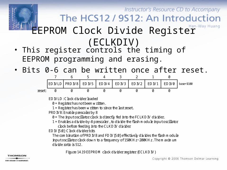
EDIVLD PRDIV8 EDIV5 EDIV4 EDIV3 EDIV2 EDIV1 EDIV0
7 6 5 4 3 2 1 0
reset: 0 0 0 0 0 0 0 0
EDIVLD: Clock divider loaded 0 = Register has not been written. 1 = Register has been written to since the last reset.PRDIV8: Enable prescaler by 8 0 = The input oscillator clock is directly fed into the FCLKDIV divider. 1 = Enables a divide-by-8 prescaler , to divide the flash module input oscillator clock before feeding into the CLKDIV dividerEDIV[5:0]: Clock divider bits The combination of PRDIV8 and FDIV[5:0] effectively divides the flash module input oscillator clock down to a frequency of 150KHz~200KHz. The maximum divide ratio is 512.
Figure 14.19 EEPROM clock divider register (ECLKDIV)
base+$100
EEPROM Clock Divide Register (ECLKDIV)• This register controls the timing of EEPROM
programming and erasing.• Bits 0-6 can be written once after reset.
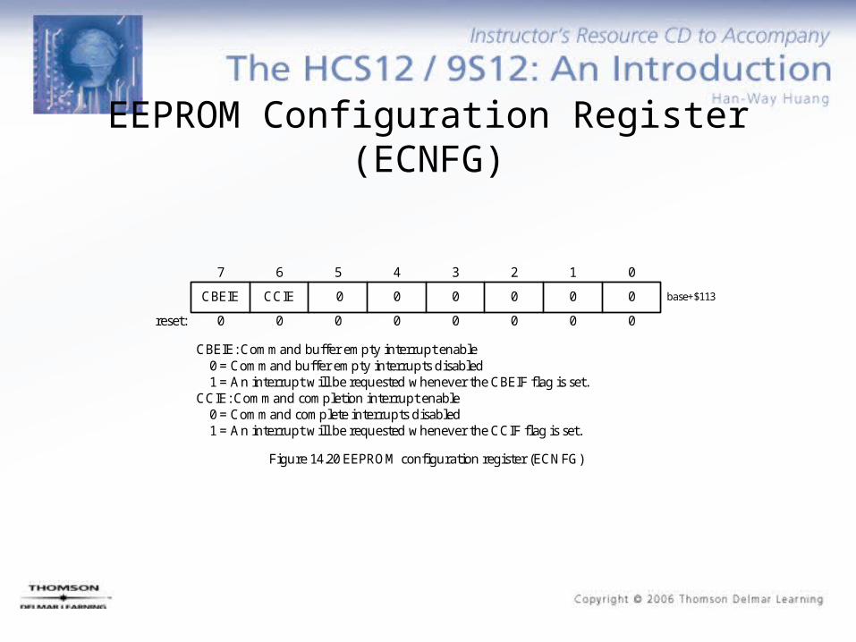
CBEIE CCIE 0 0 0 0 0 0
7 6 5 4 3 2 1 0
reset: 0 0 0 0 0 0 0 0
CBEIE: Command buffer empty interrupt enable 0 = Command buffer empty interrupts disabled 1 = An interrupt will be requested whenever the CBEIF flag is set.CCIE: Command completion interrupt enable 0 = Command complete interrupts disabled 1 = An interrupt will be requested whenever the CCIF flag is set.
Figure 14.20 EEPROM configuration register (ECNFG)
base+$113
EEPROM Configuration Register (ECNFG)

EEPROM Protection Register (EPROT) (1 of 2)
• This register defines which EEPROM sectors are protected against program or erase.
• This register is loaded from EEPROM at $_FFD in the reset sequence.
• The EP[2:0] bits can be written any time until the EPDIS bit is cleared.
• The contents of this register are shown in Figure 14.21.
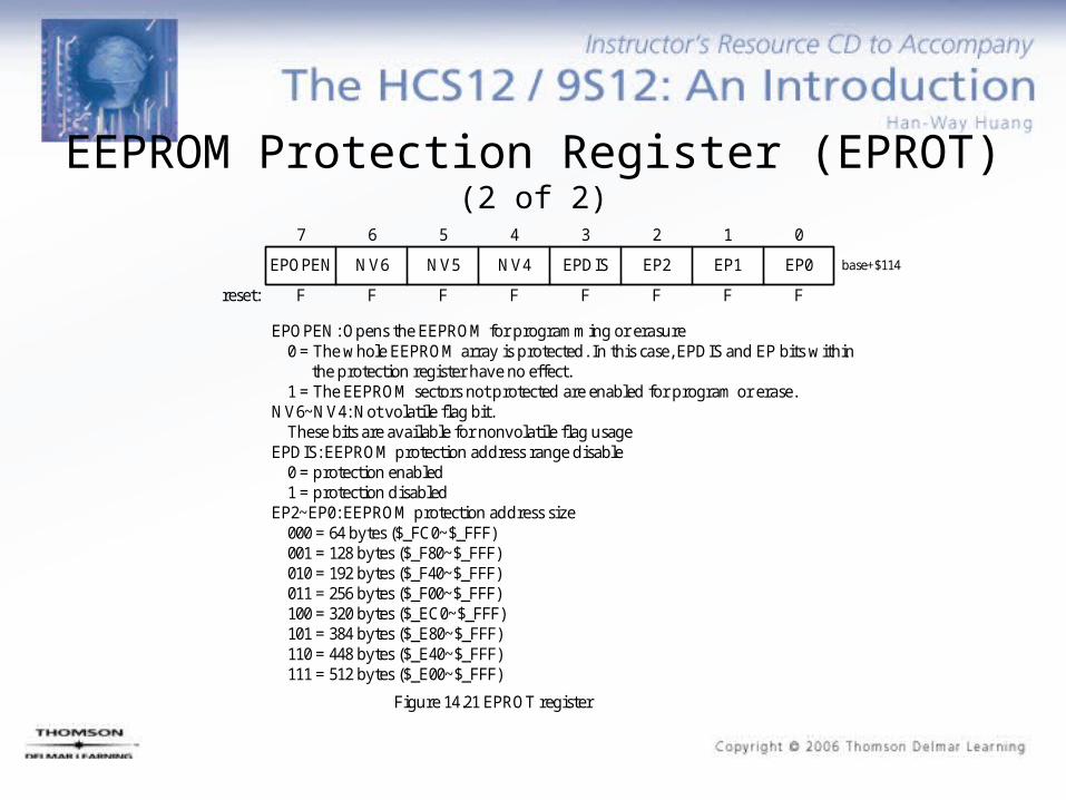
EPOPEN NV6 NV5 NV4 EPDIS EP2 EP1 EP0
7 6 5 4 3 2 1 0
reset: F F F F F F F F
EPOPEN: Opens the EEPROM for programming or erasure 0 = The whole EEPROM array is protected. In this case, EPDIS and EP bits within the protection register have no effect. 1 = The EEPROM sectors not protected are enabled for program or erase.NV6~NV4: Not volatile flag bit. These bits are available for nonvolatile flag usageEPDIS: EEPROM protection address range disable 0 = protection enabled 1 = protection disabledEP2~EP0: EEPROM protection address size 000 = 64 bytes ($_FC0~$_FFF) 001 = 128 bytes ($_F80~$_FFF) 010 = 192 bytes ($_F40~$_FFF) 011 = 256 bytes ($_F00~$_FFF) 100 = 320 bytes ($_EC0~$_FFF) 101 = 384 bytes ($_E80~$_FFF) 110 = 448 bytes ($_E40~$_FFF) 111 = 512 bytes ($_E00~$_FFF)
Figure 14.21 EPROT register
base+$114
EEPROM Protection Register (EPROT) (2 of 2)

CBEIF CCIF PVIOL ACCERR 0 BLANK 0 0
7 6 5 4 3 2 1 0
reset: 1 1 0 0 0 0 0 0
CBEIF: Command buffer empty interrupt flag 0 = Command buffers are full 1 = Command buffers are ready to accept a new commandCCIF: Command completion interrupt flag 0 = Command in progress 1 = All commands are completedPVIOL: Protection violation 0 = No failure 1 = A protection violation has occurredACCERR: Flash access error 0 = No failure 1 = Access error has occurred.BLANK: Array has been verified as erased 0 = If an erase and verify command has been requested, and the CCIF flag is set, then a zero in BLANK indicates that the block is not erased. 1 = Flash block verifies as erased.
Figure 14.22 EEPROM status register (ESTAT)
base+$115
EEPROM Status Register (ESTAT)• The bits CBEIF, PVIOL, and ACCERR are readable and
writable, bits CCIF and BLANK are readable but not writable.
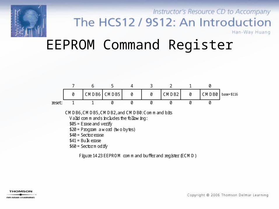
0 CMDB6 CMDB5 0 0 CMDB2 0 CMDB0
7 6 5 4 3 2 1 0
reset: 1 1 0 0 0 0 0 0
CMDB6, CMDB5, CMDB2, and CMDB0: Command bits Valid commands includes the following: $05 = Erase and verify $20 = Program a word (two bytes) $40 = Sector erase $41 = Bulk erase $60 = Sector modify
Figure 14.23 EEPROM command buffer and register (ECMD)
base+$116
EEPROM Command Register

Configuring the ECLKDIV Register
• The configuration method of this register is identical to that of the FCLKDIV register.
Programming and Erasure of EEPROM
• The programming algorithm for EEPROM is almost identical to that of the flash memory.
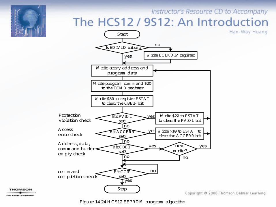
Start
Is EDIVLD bit set?
Write ECLKDIV register
Write array address andprogram data
no
yes
Write program command $20to the ECMD register
Write $80 to register ESTATto clear the CBEIF bit
Bit PVIOLset?
Bit ACCERRset?
Bit CBEIFset?
Bit CCIFset?
Stop
Write $20 to ESTATto clear the PVIOL bit
Write $10 to ESTAT toclear the ACCERR bit
nextwrite?
yes
no
yes
no
Protectionviolation check
Accesserror check
Address, data,command bufferempty check
commandcompletion checck
Figure 14.24 HCS12 EEPROM program algorithm
yes
yes
yes
no
no
no

• Example 14.10 Write a function that erase a sector (4 bytes) of EEPROM. Index register X contains a word-aligned EEPROM address within the sector to be erased.• Solution:
eraseEEsectormovb #ACCERR+PVIOL,ESTAT ; clear error flagsbrclr ESTAT,CBEIF,EERErr ; command buffer not empty, returnstd 0,X ; write any data to EEPROM sectormovb #SectorErase,ECMD ; write sector erase commandmovb #CBEIF,ESTAT ; launch erase commandbrclr ESTAT,ACCERR+PVIOL,EEROK ; no error?
EERErr ldab #1 ; error code set to 1rts
EEROK brclr ESTAT,CCIF,EEROK ; wait until command completionclrbrts
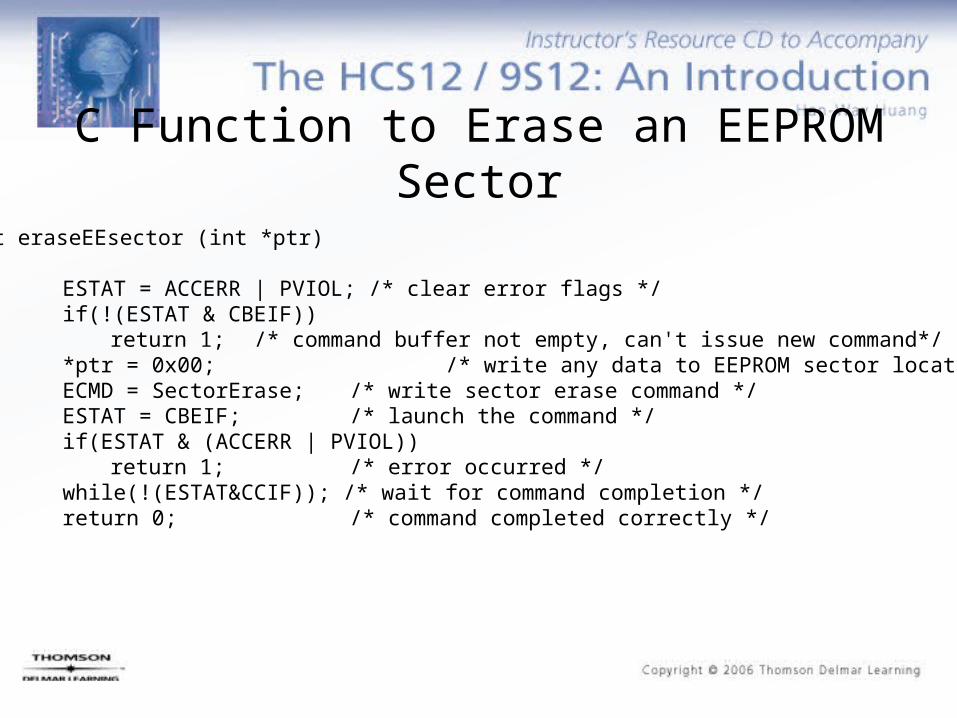
int eraseEEsector (int *ptr){ ESTAT = ACCERR | PVIOL; /* clear error flags */ if(!(ESTAT & CBEIF)) return 1; /* command buffer not empty, can't issue new command*/ *ptr = 0x00; /* write any data to EEPROM sector location */ ECMD = SectorErase; /* write sector erase command */ ESTAT = CBEIF; /* launch the command */ if(ESTAT & (ACCERR | PVIOL)) return 1; /* error occurred */ while(!(ESTAT&CCIF)); /* wait for command completion */ return 0; /* command completed correctly */}
C Function to Erase an EEPROM Sector
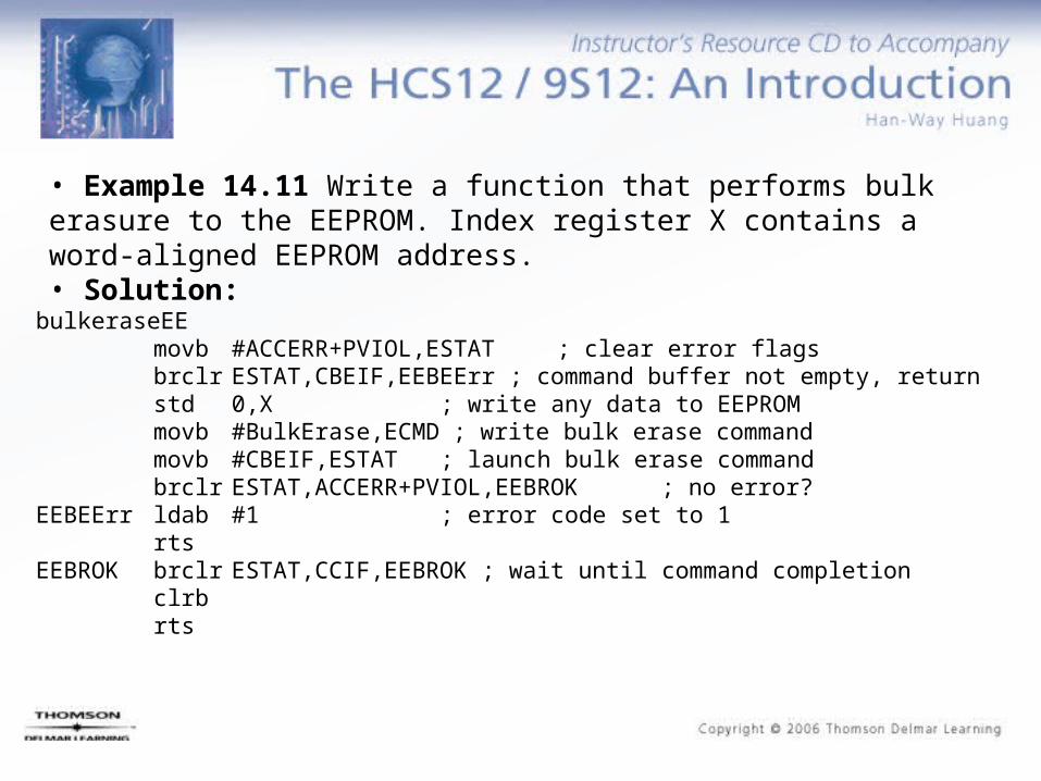
• Example 14.11 Write a function that performs bulk erasure to the EEPROM. Index register X contains a word-aligned EEPROM address.• Solution:
bulkeraseEEmovb #ACCERR+PVIOL,ESTAT ; clear error flagsbrclr ESTAT,CBEIF,EEBEErr ; command buffer not empty, returnstd 0,X ; write any data to EEPROM movb #BulkErase,ECMD ; write bulk erase commandmovb #CBEIF,ESTAT ; launch bulk erase commandbrclr ESTAT,ACCERR+PVIOL,EEBROK ; no error?
EEBEErr ldab #1 ; error code set to 1rts
EEBROK brclr ESTAT,CCIF,EEBROK ; wait until command completionclrbrts
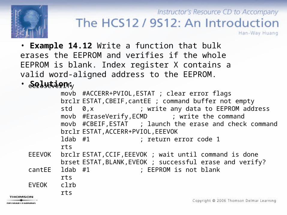
• Example 14.12 Write a function that bulk erases the EEPROM and verifies if the whole EEPROM is blank. Index register X contains a valid word-aligned address to the EEPROM.• Solution:
eeraseverifymovb #ACCERR+PVIOL,ESTAT ; clear error flagsbrclr ESTAT,CBEIF,cantEE ; command buffer not emptystd 0,x ; write any data to EEPROM addressmovb #EraseVerify,ECMD; write the commandmovb #CBEIF,ESTAT ; launch the erase and check commandbrclr ESTAT,ACCERR+PVIOL,EEEVOKldab #1 ; return error code 1rts
EEEVOK brclr ESTAT,CCIF,EEEVOK ; wait until command is donebrset ESTAT,BLANK,EVEOK ; successful erase and verify?
cantEE ldab #1 ; EEPROM is not blankrts
EVEOK clrbrts
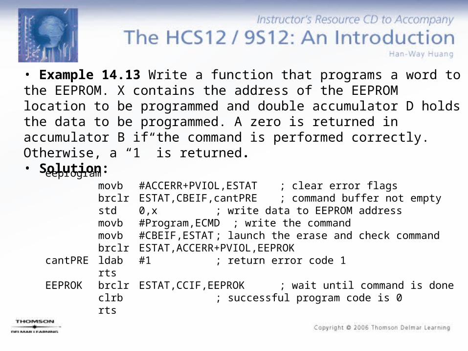
• Example 14.13 Write a function that programs a word to the EEPROM. X contains the address of the EEPROM location to be programmed and double accumulator D holds the data to be programmed. A zero is returned in accumulator B if the command is performed correctly. Otherwise, a “1” is returned.• Solution:
eeprogrammovb #ACCERR+PVIOL,ESTAT ; clear error flagsbrclr ESTAT,CBEIF,cantPRE ; command buffer not emptystd 0,x ; write data to EEPROM addressmovb #Program,ECMD ; write the commandmovb #CBEIF,ESTAT ; launch the erase and check commandbrclr ESTAT,ACCERR+PVIOL,EEPROK
cantPRE ldab #1 ; return error code 1rts
EEPROK brclr ESTAT,CCIF,EEPROK ; wait until command is doneclrb ; successful program code is 0rts
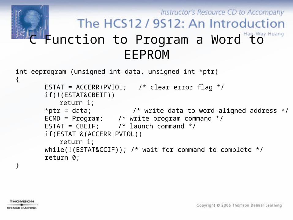
int eeprogram (unsigned int data, unsigned int *ptr){ ESTAT = ACCERR+PVIOL; /* clear error flag */ if(!(ESTAT&CBEIF)) return 1; *ptr = data; /* write data to word-aligned address */ ECMD = Program; /* write program command */ ESTAT = CBEIF; /* launch command */ if(ESTAT &(ACCERR|PVIOL)) return 1; while(!(ESTAT&CCIF)); /* wait for command to complete */ return 0;}
C Function to Program a Word to EEPROM
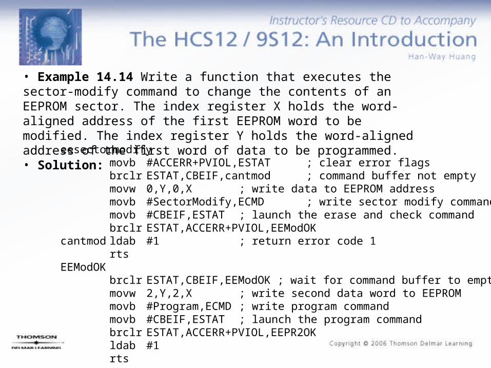
• Example 14.14 Write a function that executes the sector-modify command to change the contents of an EEPROM sector. The index register X holds the word-aligned address of the first EEPROM word to be modified. The index register Y holds the word-aligned address of the first word of data to be programmed.• Solution: eesectormodify
movb #ACCERR+PVIOL,ESTAT ; clear error flagsbrclr ESTAT,CBEIF,cantmod ; command buffer not emptymovw 0,Y,0,X ; write data to EEPROM addressmovb #SectorModify,ECMD ; write sector modify commandmovb #CBEIF,ESTAT ; launch the erase and check commandbrclr ESTAT,ACCERR+PVIOL,EEModOK
cantmod ldab #1 ; return error code 1rts
EEModOKbrclr ESTAT,CBEIF,EEModOK ; wait for command buffer to emptymovw 2,Y,2,X ; write second data word to EEPROM movb #Program,ECMD ; write program commandmovb #CBEIF,ESTAT ; launch the program commandbrclr ESTAT,ACCERR+PVIOL,EEPR2OKldab #1rts

EEPR2Ok brclr ESTAT,CCIF,EEPR2OK; wait for command completionclrb ; successful program code is 0rts
int EESectorModify(unsigned int *src, unsigned int *dest){ ESTAT = ACCERR | PVIOL; /* clear error flags */ if(!(ESTAT&CBEIF)) return 1; /* command buffer not empty is error */ *dest = *src; /* write first data word */ ECMD = SectorModify; /* write sector modify command */ ESTAT = CBEIF; /* launch the sector modify command */ if(ESTAT&(ACCERR | PVIOL)) return 1; /* command failed */ while(!(ESTAT&CBEIF)); /* wait for command buffer becomes empty */ *(dest+1) = *(src+1); /* write second data word */ ECMD = Program; /* write the program command */ ESTAT = CBEIF; /* launch the program command */ if(ESTAT&(ACCERR | PVIOL)) return 1; /* command failed */ while(!(ESTAT&CCIF)); /* wait for command buffer becomes empty */ return 0;}

HCS12 External Interface (1 of 3)
• External memory interface is implemented across four I/O ports (A, B, E, and K).• External memory signal pins are listed in Table 14.7.• Signals ADDR0…ADDR15 and XADDR14…XADDR19 are used to select a memory
location to access and are referred to as the address bus.• DATA0…DATA15 are used to carry data and hence are referred to as the data bus.• When the external memory is not paged, only the lower 16 address/data pins are
used.• If expanded memory is enabled, then ADDR14 and ADDR15 are not used.• A0…A15 are used instead of ADDR0…ADDR15.• D0…D15 are used instead of DATA0…DATA15.• XA14…XA19 are used instead of XADDR14…XADDR19.• R/W signal is used to indicate the direction of data transfer.• LSTRB signal is used to indicate whether the lower data bus (D7…D0) carries valid
data.• In expanded narrow mode, external memory data pins are connected to D15…D8.• LSTRB, R/W, and A0 interface the type of bus access that is taking place.

Table 14.7 HCS12 external memory interface signal pins
Signal name Function
ADDR0/ DATA0ADDR1/ DATA1ADDR2/ DATA2ADDT3/ DATA3ADDT4/ DATA4ADDT5/ DATA5ADDT6/ DATA6ADDT7/ DATA7ADDR8/ DATA8ADDR9/ DATA9ADDR10/ DATA10ADDT11/ DATA11ADDT12/ DATA12ADDT13/ DATA13ADDT14/ DATA14ADDT15/ DATA15XADDR14XADDR15XADDR16XADDR17XADDR18XADDR19R/ WLSTRBECLKECS/ ROMONEXCS
EMI address bit 0 or data bit 0EMI address bit 1 or data bit 1EMI address bit 2 or data bit 2EMI address bit 3 or data bit 3EMI address bit 4 or data bit 4EMI address bit 5 or data bit 5EMI address bit 6 or data bit 6EMI address bit 7 or data bit 7EMI address bit 8 or data bit 8EMI address bit 9 or data bit 9EMI address bit 10 or data bit 10EMI address bit 11 or data bit 11EMI address bit 12 or data bit 12EMI address bit 13 or data bit 13EMI address bit 14 or data bit 14EMI address bit 15 or data bit 15EMI extended address bit 14EMI extended address bit 15EMI extended address bit 16EMI extended address bit 17EMI extended address bit 18EMI extended address bit 19Read/ writelower byte strobeE clockEmulated chip select/ on-chip ROM enableExternal data chip select
Note. EMI stands for external memory interface
HCS12 External Interface (2 of 3)
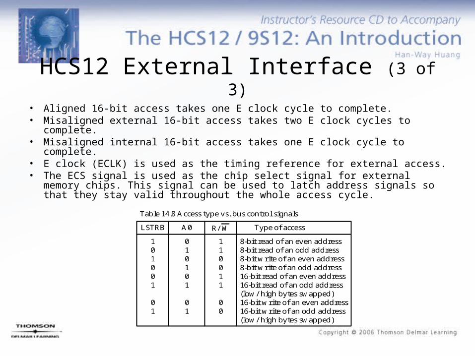
Table 14.8 Access type vs. bus control signals
LSTRB A0 R/ W Type of access
101001
01
010101
01
110011
00
8-bit read of an even address8-bit read of an odd address8-bit write of an even address8-bit write of an odd address16-bit read of an even address16-bit read of an odd address(low/ high bytes swapped)16-bit write of an even address16-bit write of an odd address(low/ high bytes swapped)
HCS12 External Interface (3 of 3)
• Aligned 16-bit access takes one E clock cycle to complete.• Misaligned external 16-bit access takes two E clock cycles to complete.• Misaligned internal 16-bit access takes one E clock cycle to complete.• E clock (ECLK) is used as the timing reference for external access.• The ECS signal is used as the chip select signal for external memory chips.
This signal can be used to latch address signals so that they stay valid throughout the whole access cycle.

trtf
0.9VDD0.9VDD
0.1VDD0.1VDD
Figure 14.25 A typical digital waveform
Waveforms of Bus Signals (1 of 3)
• The waveform of a typical digital signal is shown.
• The rise time (tr) of a signal is the time needed for a signal to rise from 10% of the power supply voltage to 90% of the power supply voltage.
• The fall time (tf) of a signal is the time needed for a signal to drop from 90% of the power supply voltage to 10% of the power supply voltage.
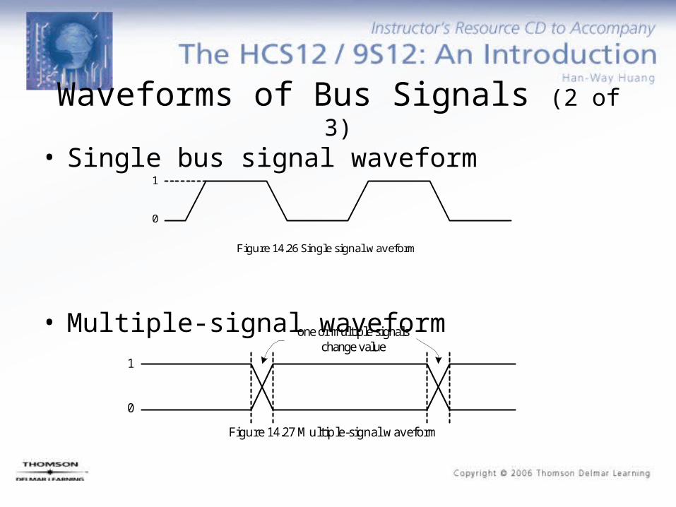
1
0
Figure 14.26 Single signal waveform
1
0
Figure 14.27 Multiple-signal waveform
one or multiple signalschange value
Waveforms of Bus Signals (2 of 3)
• Single bus signal waveform
• Multiple-signal waveform

unknown(a)
unknown
(b)
Figure 14.28 Unknown signals. (a) single signal. (b) multiple signal.
signal floating
signal floating
(a)
(b)
Figure 14.29 Floating signals. (a) Single signal. (b) Multiple signals.
Waveforms of Bus Signals (3 of 3)
• Unknown signal
• Floating signals
Categories of Bus Signals
• Address• Data• Control
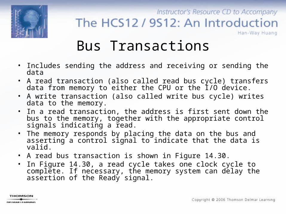
Bus Transactions• Includes sending the address and receiving or sending the data• A read transaction (also called read bus cycle) transfers data from
memory to either the CPU or the I/O device.• A write transaction (also called write bus cycle) writes data to the
memory. • In a read transaction, the address is first sent down the bus to the
memory, together with the appropriate control signals indicating a read.
• The memory responds by placing the data on the bus and asserting a control signal to indicate that the data is valid.
• A read bus transaction is shown in Figure 14.30.• In Figure 14.30, a read cycle takes one clock cycle to complete. If
necessary, the memory system can delay the assertion of the Ready signal.
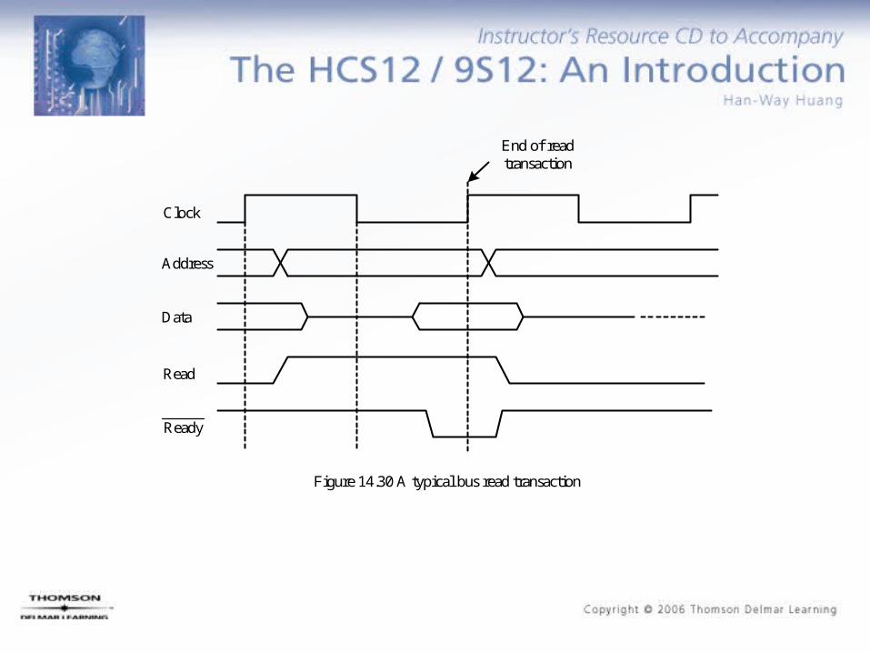
End of readtransaction
Clock
Address
Data
Read
Figure 14.30 A typical bus read transaction
Ready

Address
Data
Read
Request
ACK
Master asserts address
Slave drives data
Figure 14.31 Asynchroous read bus transaction.
Terminology• Bus master
– A device that can generate address and control signals during a bus transaction
• Bus slave– A device such as a memory
chip that can only respond to the bus transaction
• Synchronous bus– A bus that uses a clock
signal to synchronize bus transactions
• Asynchronous bus– A bus that does not use a
clock signal to synchronize the bus transaction
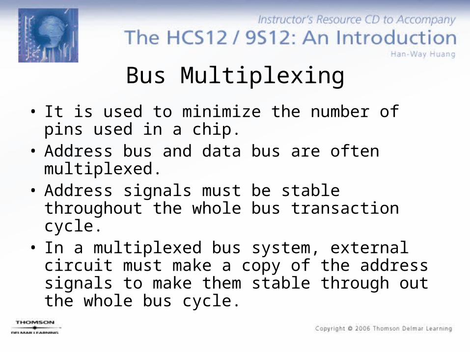
Bus Multiplexing
• It is used to minimize the number of pins used in a chip.
• Address bus and data bus are often multiplexed.• Address signals must be stable throughout the
whole bus transaction cycle.• In a multiplexed bus system, external circuit
must make a copy of the address signals to make them stable through out the whole bus cycle.

The HCS12 Bus Cycles
• The timing diagrams of a read and a write bus cycle are combined in Figure 14.32.
• Figure 14.32 shows that a bus cycle starts with the MCU driving the address signals onto the address bus.
• The events that occur during a read cycle are illustrated in Figure 14.33.
• The events that occur during a write a cycle are illustrate in Figure 14.34.

35
3 4
1, 2
363433IPIPE0IPIPE1
NOACC
30 31 32
29
26
2322
19
13
11
27
24 25
28
20 21
17 18
12 1487
615
10169
5ECLK
LSTRB
R/W
ECS
XA19:XA14
Addr/Data(write)
Addr/Data(read)
addr
addr
data
data
Figure 14.32 The HCS12 Read/Write bus cycle timing diagram
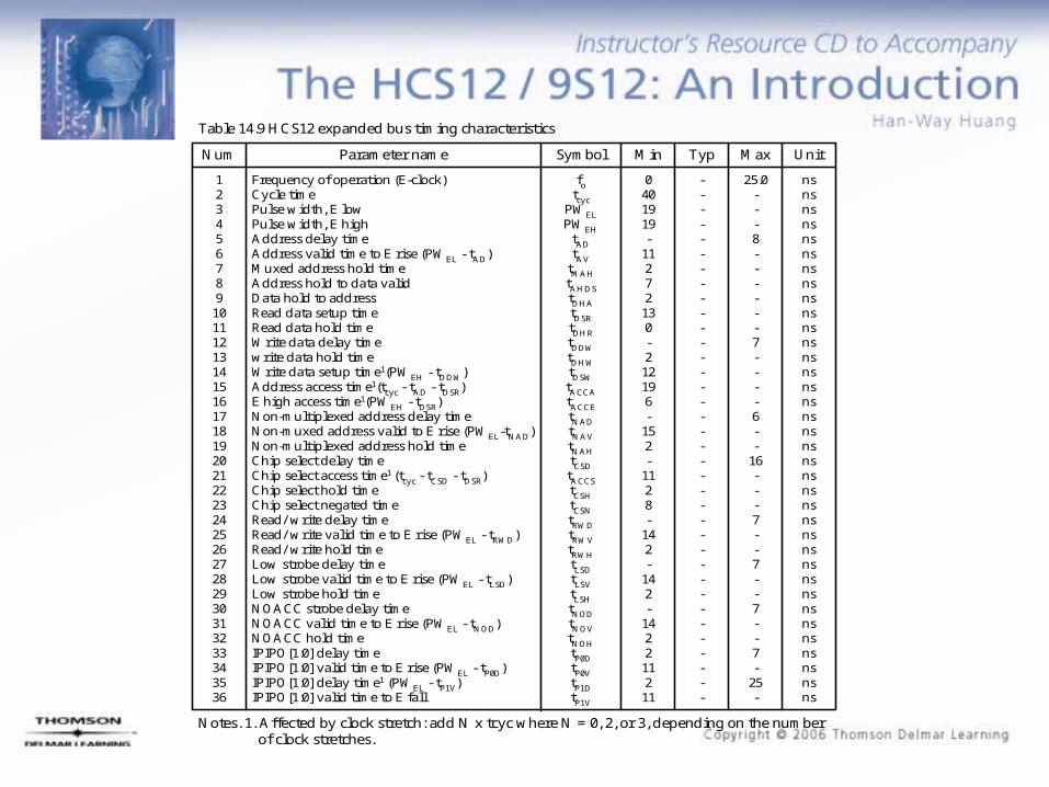
Table 14.9 HCS12 expanded bus timing characteristics
Num Parameter name Symbol UnitMin Typ Max
123456789101112131415161718192021222324252627282930313233343536
Frequency of operation (E-clock)Cycle timePulse width, E lowPulse width, E highAddress delay timeAddress valid time to E rise (PWEL - tAD)Muxed address hold timeAddress hold to data validData hold to addressRead data setup timeRead data hold timeWrite data delay timewrite data hold timeWrite data setup time1(PWEH - tDDW)Address access time1(tcyc - tAD - tDSR)E high access time1(PWEH - tDSR)Non-multiplexed address delay timeNon-muxed address valid to E rise (PWEL-tNAD)Non-multiplexed address hold timeChip select delay timeChip select access time1 (tcyc - tCSD - tDSR)Chip select hold timeChip select negated timeRead/ write delay timeRead/ write valid time to E rise (PWEL - tRWD)Read/ write hold timeLow strobe delay timeLow strobe valid time to E rise (PWEL - tLSD)Low strobe hold timeNOACC strobe delay timeNOACC valid time to E rise (PWEL - tNOD)NOACC hold timeIPIPO[1:0] delay timeIPIPO[1:0] valid time to E rise (PWEL - tP0D)IPIPO[1:0] delay time1 (PWEL - tP1V)IPIPO[1:0] valid time to E fall
fotcyc
PWELPWEHtADtAV
tMAHtAHDStDHAtDSRtDHRtDDWtDHWtDSWtACCAtACCEtNADtNAVtNAHtCSDtACCStCSHtCSNtRWDtRWVtRWHtLSDtLSVtLSHtNODtNOVtNOHtP0DtP0VtP1DtP1V
0401919-
11272130-212196-
152-
1128-
142-
142-
142211211
25.0---8------7----6--
16---7--7--7--7-
25-
nsnsnsnsnsnsnsnsnsnsnsnsnsnsnsnsnsnsnsnsnsnsnsnsnsnsnsnsnsnsnsnsnsnsnsns
Notes. 1. Affected by clock stretch: add N x tcyc where N = 0, 2, or 3, depending on the number of clock stretches.
------------------------------------
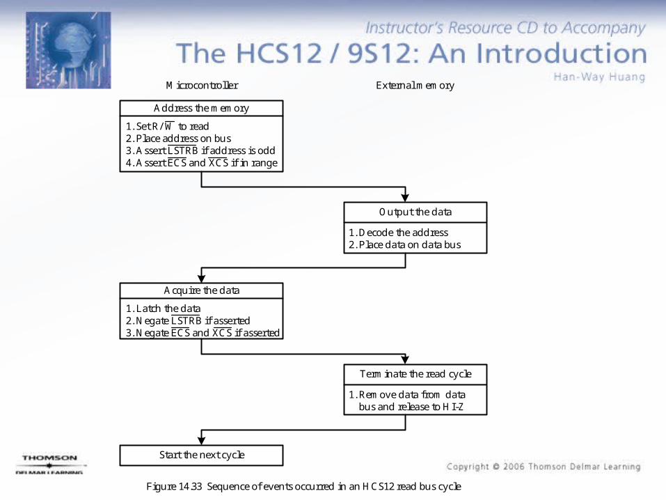
1. Set R/ W to read2. Place address on bus3. Assert LSTRB if address is odd4. Assert ECS and XCS if in range
Address the memory
Output the data
1. Decode the address2. Place data on data bus
Microcontroller External memory
1. Latch the data2. Negate LSTRB if asserted3. Negate ECS and XCS if asserted
Acquire the data
Terminate the read cycle
1. Remove data from data bus and release to HI-Z
Start the next cycle
Figure 14.33 Sequence of events occurred in an HCS12 read bus cycle
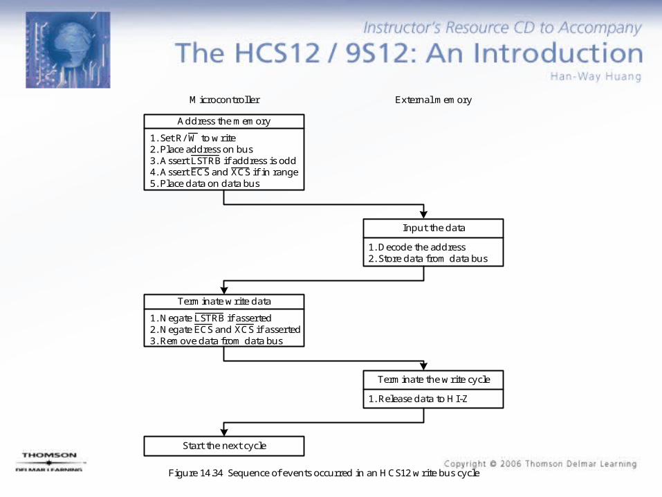
1. Set R/ W to write2. Place address on bus3. Assert LSTRB if address is odd4. Assert ECS and XCS if in range5. Place data on data bus
Address the memory
Input the data
1. Decode the address2. Store data from data bus
Microcontroller External memory
1. Negate LSTRB if asserted2. Negate ECS and XCS if asserted3. Remove data from data bus
Terminate write data
Terminate the write cycle
1. Release data to HI-Z
Start the next cycle
Figure 14.34 Sequence of events occurred in an HCS12 write bus cycle
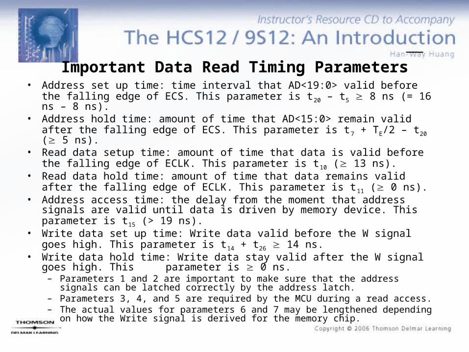
Important Data Read Timing Parameters• Address set up time: time interval that AD<19:0> valid before the falling
edge of ECS. This parameter is t20 – t5 8 ns (= 16 ns – 8 ns).• Address hold time: amount of time that AD<15:0> remain valid after the
falling edge of ECS. This parameter is t7 + TE/2 – t20 ( 5 ns).• Read data setup time: amount of time that data is valid before the falling
edge of ECLK. This parameter is t10 ( 13 ns).• Read data hold time: amount of time that data remains valid after the falling
edge of ECLK. This parameter is t11 ( 0 ns).• Address access time: the delay from the moment that address signals are
valid until data is driven by memory device. This parameter is t15 (> 19 ns).• Write data set up time: Write data valid before the W signal goes high. This
parameter is t14 + t26 14 ns.• Write data hold time: Write data stay valid after the W signal goes high. This
parameter is 0 ns.– Parameters 1 and 2 are important to make sure that the address signals can be
latched correctly by the address latch.– Parameters 3, 4, and 5 are required by the MCU during a read access.– The actual values for parameters 6 and 7 may be lengthened depending on how
the Write signal is derived for the memory chip.

Issues Related to Adding External Memory
• Memory space assignment• Address decoder and control circuitry design• Timing verification
Memory Space Assignment
• Equal size assignment– The available memory space is divided into blocks of equal size.– Each block is assigned to a memory device without regarding for
the actual size of each memory-mapped device.– Memory space tends to be wasted using this approach because
most memory-mapped peripheral chips need only a few bytes to be assigned to their internal registers.
• Demand assignment – The user assigns the memory space according to the size of
memory devices.
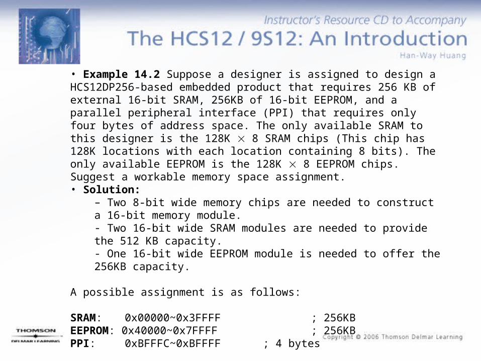
• Example 14.2 Suppose a designer is assigned to design a HCS12DP256-based embedded product that requires 256 KB of external 16-bit SRAM, 256KB of 16-bit EEPROM, and a parallel peripheral interface (PPI) that requires only four bytes of address space. The only available SRAM to this designer is the 128K 8 SRAM chips (This chip has 128K locations with each location containing 8 bits). The only available EEPROM is the 128K 8 EEPROM chips. Suggest a workable memory space assignment.• Solution:
– Two 8-bit wide memory chips are needed to construct a 16-bit memory module. - Two 16-bit wide SRAM modules are needed to provide the 512 KB capacity. - One 16-bit wide EEPROM module is needed to offer the 256KB capacity.
A possible assignment is as follows:
SRAM: 0x00000~0x3FFFF ; 256KBEEPROM: 0x40000~0x7FFFF ; 256KBPPI: 0xBFFFC~0xBFFFF ; 4 bytes

Address Decoder Design • Address decoder selects one and only one memory device to
respond to the memory access request.• All memory devices have control signals such as chip-enable (CE),
chip-select (CS), or output-enable (OE) to control their read and write operations.
• Two address-decoding schemes have been used:– Full decoding– Partial decoding
• Address decoder design is closely related to memory space assignment.
• The programmable logic devices (PLDs) make full decoding easy and flexible.
• GALs and PALs are often used to implement address decoders.
Timing Verification • In a read cycle, the most critical timing requirements are
the data setup time and data hold time required by the microcontroller.
• The address setup time and hold time requirements for the memory devices are also critical.
• In a write cycle, the most critical timing requirements are the write data setup time and write data hold time required by the memory device.
• The address setup time and hold time must also be satisfied.
• For a write cycle, the write pulse width must be long enough for the write cycle to be successful.
Memory Devices
• The control circuit designs for interfacing the SRAM, the EPROM, the EEPROM, and the FLASH memory to the HCS12 MCU are quite similar.

The K6R1008C1D (1 of 4)
• A 128K 8 SRAM asynchronous SRAM from Samsung that operates with 5V power supply– Has short access time (10 ns) and three-state output– Has automatic power-down feature to reduce power
consumption– The address signals A16-A0 select one of the 128K locations on
the chip.– The CS signal enables read/write access to the K6R1008C1D. – The OE signal is the output enable. If OE is high, I/O pins will be
in high-impedance.– Depending on the assertion times of control signals, there are
two timing diagrams for the read cycle and three timing diagrams for the write cycle

A0
A1
A2
A3
CS
A4
VCC
VSS
I/O1
I/O2
I/O3
A5
A16
A15
A14
A13
A11
A12
VSS
VCC
I/O8
I/O7
I/O6
I/O5I/O4
K6RC1008C1D
1
2
3
4
5
6
7
8
9
10
11
12
13
14 19
20
21
22
23
24
25
26
27
28
29
30
31
32
Figure 14.35 The K6R1008C1D pin assignment
15
16
18
17
OE
A10
A9
A8A7
A6
WE
The K6R1008C1D (2 of 4)
tRC
tAAtOH
Address
Data Valid DataPrevious Valid Data
(a) Read Cycle 1 (OE and CE are asserted in the whole cycle)
tPD
tDH
tOHZ
tRC
Address
Data
CS
OE tOE
tOLZ
tLZ(4,5)
tPU
Valid Data
VCCcurrent
(b) Read Cycle No. 2 (OE controlled)
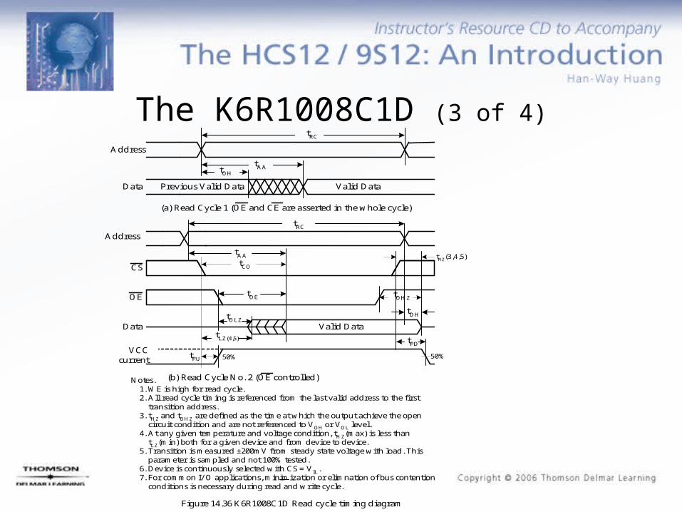
Figure 14.36 K6R1008C1D Read cycle timing diagram
tAA
tCO
50% 50%
tHZ(3,4,5)
Notes. 1. WE is high for read cycle. 2. All read cycle timing is referenced from the last valid address to the first transition address. 3. tHZ and tOHZ are defined as the time at which the output achieve the open circuit condition and are not referenced to VOH or VOL level. 4. At any given temperature and voltage condition, tHZ(max) is less than tLZ(min) both for a given device and from device to device. 5. Transition is measured ±200mV from steady state voltage with load. This parameter is sampled and not 100% tested. 6. Device is continuously selected with CS = VIL. 7. For common I/ O applications, minimization or elimnation of bus contention conditions is necessary during read and write cycle.
The K6R1008C1D (3 of 4)

The K6R1008C1D (4 of 4)
• In Figure 14.36a and 14.36b, the CS signal must be asserted (low) for at least tRC ns during a read cycle.
• The signal that is asserted the latest determines the time that data will become valid.
• In Figure 14.36b, the OE signal is asserted the latest, data becomes available tOE ns later.
• Data pins will go to high-impedance state tOHZ ns after the OE signal goes to high or tHZ ns after the CS signal goes to high.
tWC
tAW
tCW
tWP
tDW tDH
tOHZ
tAS
tWR
valid data
High-Z
Address
OE
CS
WE
Data In
Data Out
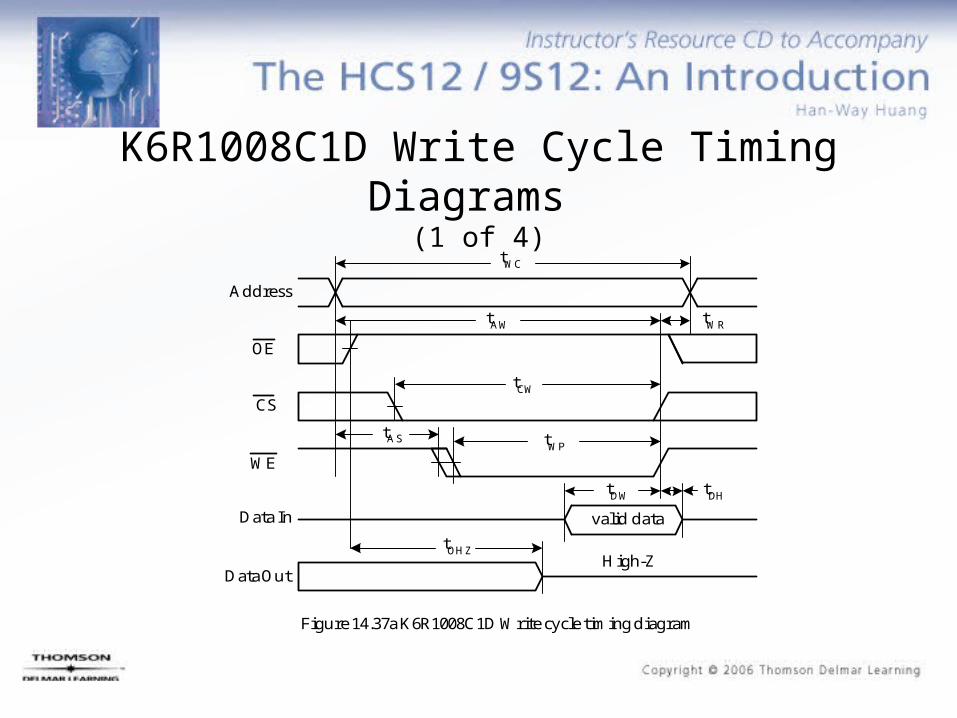
Figure 14.37a K6R1008C1D Write cycle timing diagram
K6R1008C1D Write Cycle Timing Diagrams (1 of 4)

tWC
tAW
tCW
tWP
tDW tDH
tWHZ
tAS
tWR
valid data
High-Z
Address
CS
WE
Data In
Data Out
Figure 14.37b K6R1008C1D Write cycle timing diagram (OE tied to low)
tOW
- When both CS and WE are deasserted (goes to high), Data Out pins get out of the high impedance state.
K6R1008C1D Write Cycle Timing Diagrams (2 of 4)

tWC
tAW
tCW
tWP
tDW tDH
tAS
tWR
valid data
Address
CS
WE
Data In
Figure 14.37c K6R1008C1D Write cycle timing diagram(CS controlled)
K6R1008C1D Write Cycle Timing Diagrams (3 of 4)
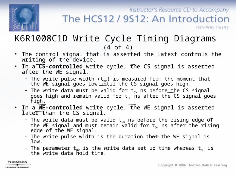
K6R1008C1D Write Cycle Timing Diagrams (4 of 4)
• The control signal that is asserted the latest controls the writing of the device.
• In a CS-controlled write cycle, the CS signal is asserted after the WE signal.– The write pulse width (tWP) is measured from the moment that the WE
signal goes low until the CS signal goes high.– The write data must be valid for tDW ns before the CS signal goes high
and remain valid for tDH ns after the CS signal goes high.• In a WE-controlled write cycle, the WE signal is asserted later than
the CS signal.– The write data must be valid tDW ns before the rising edge of the WE
signal and must remain valid for tDH ns after the rising edge of the WE signal.
– The write pulse width is the duration that the WE signal is low.– The parameter tDW is the write data set up time whereas tDH is the write
data hold time.
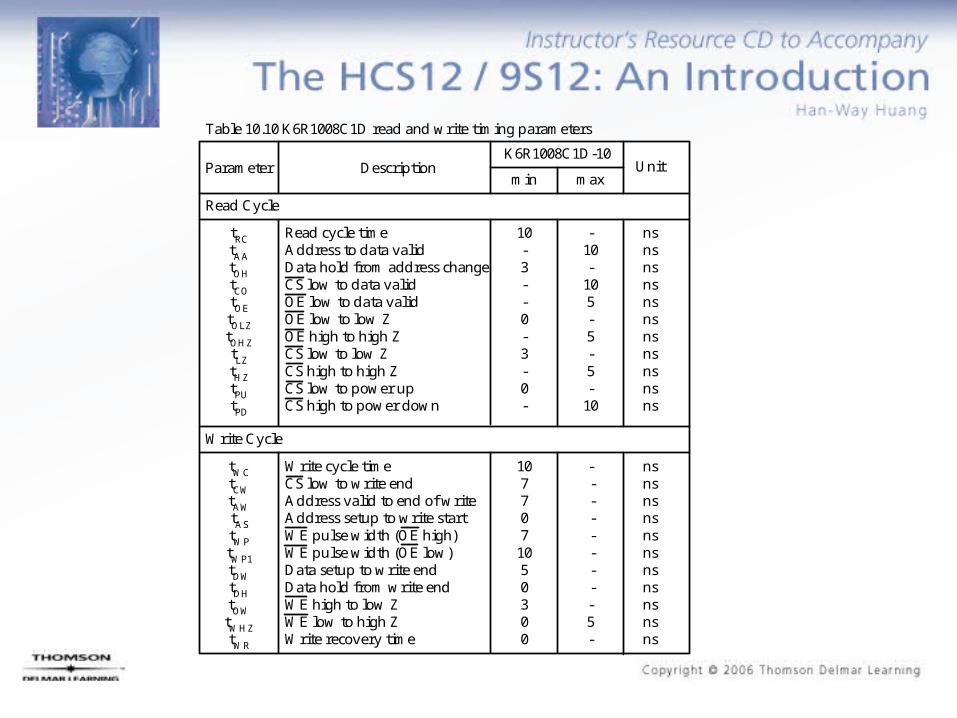
Parameter Description
tRCtAAtOHtCOtOEtOLZtOHZtLZtHZtPUtPD
Read cycle timeAddress to data validData hold from address changeCS low to data validOE low to data validOE low to low ZOE high to high ZCS low to low ZCS high to high ZCS low to power upCS high to power down
K6R1008C1D-10
min max
10-3--0-3-0-
Unit
-10-
105-5-5-
10
nsnsnsnsnsnsnsnsnsnsns
tWCtCWtAWtAStWPtWP1tDWtDHtOWtWHZtWR
Write cycle timeCS low to write endAddress valid to end of writeAddress setup to write startWE pulse width (OE high)WE pulse width (OE low)Data setup to write endData hold from write endWE high to low ZWE low to high ZWrite recovery time
1077071050300
- - - - - - - --5-
nsnsnsnsnsnsnsnsnsnsns
Write Cycle
Read Cycle
Table 10.10 K6R1008C1D read and write timing parameters
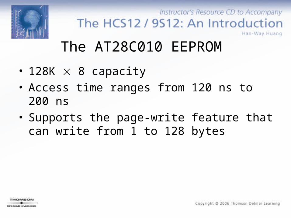
The AT28C010 EEPROM
• 128K 8 capacity• Access time ranges from 120 ns to 200 ns• Supports the page-write feature that can write
from 1 to 128 bytes
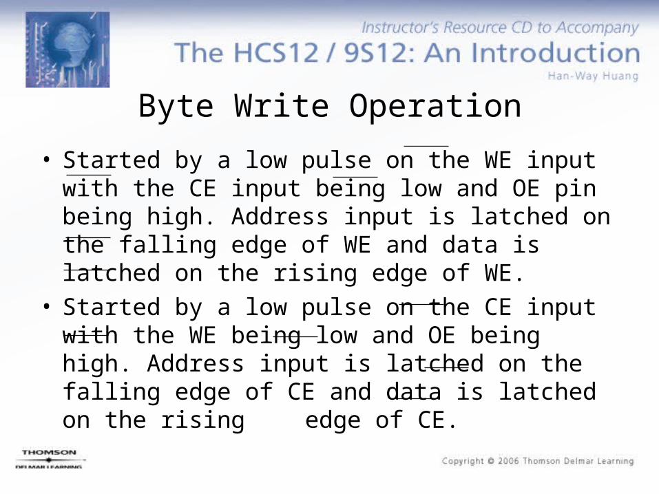
Byte Write Operation
• Started by a low pulse on the WE input with the CE input being low and OE pin being high. Address input is latched on the falling edge of WE and data is latched on the rising edge of WE.
• Started by a low pulse on the CE input with the WE being low and OE being high. Address input is latched on the falling edge of CE and data is latched on the rising edge of CE.
Page-Write Operation• Started in the same manner as in byte write operation.• Each successive byte must be loaded within 150 s (tBLC)
of the previous byte. • If the tBLC limit is exceeded, the AT28C010 will cease
accepting data and begin the internal programming operation.
• All bytes involved in a page-write operation must reside on the same page as defined by the state of the A16-A7 inputs.
• For each high-to-low transition of the signal during the page-write operation, the address signals A16-A7 must be the same.
Detecting the End of an Internal Write Operation
• Poll the I/O7 pin.• Before internal write is complete, the I/O7 shows
the complement of the value last written into it.• Successive attempts to read data from the
device will result in I/O6 toggling between 1 and 0.
Data Protection
• Both hardware and software features are provided to protect the memory against inadvertent write operations.
• Hardware protection method:– VCC sense. If VCC is below 3.8V, the write function is inhibited. – VCC power on delay. Once VCC has reached 3.8V, the device
will automatically time out for 5 ms before allowing a write operation.
– Write inhibit. Holding the OE signal low, or the CE signal high, or the WE signal high inhibits write cycles.
– Noise filter. Pulses of less than 15 ns on the WE or the CE input will not initiate a write cycle.
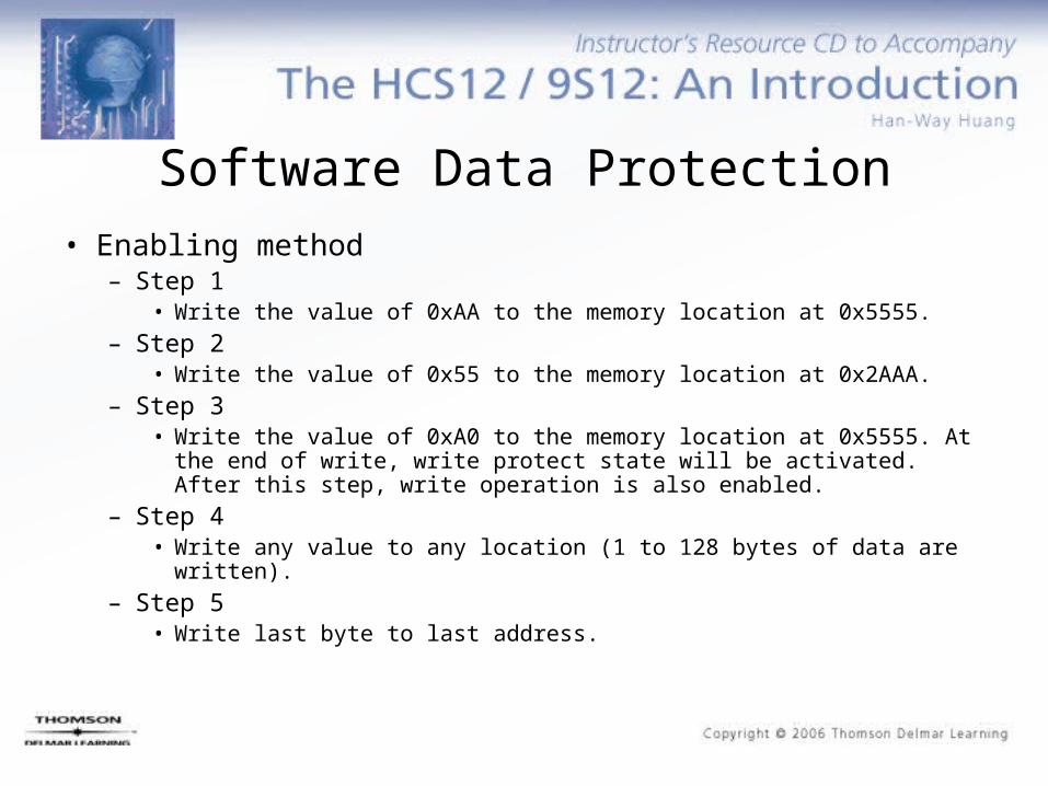
Software Data Protection
• Enabling method– Step 1
• Write the value of 0xAA to the memory location at 0x5555.
– Step 2• Write the value of 0x55 to the memory location at 0x2AAA.
– Step 3• Write the value of 0xA0 to the memory location at 0x5555. At the
end of write, write protect state will be activated. After this step, write operation is also enabled.
– Step 4• Write any value to any location (1 to 128 bytes of data are written).
– Step 5• Write last byte to last address.

Method for Disabling Software Data Protection
• Step 1– Write the value of 0xAA to the memory location at 0x5555.
• Step 2– Write the value of 0x55 to the memory location at 0x2AAA.
• Step 3– Write the value of 0x80 to the memory location at 0x5555.
• Step 4– Write the value of 0xAA to the memory location at 0x5555.
• Step 5– Write the value of 0x55 to the memory location at 0x2AAA.
• Step 6– Write the value of 0x20 to the memory location at 0x5555. After this step, software data
protection is exited.• Step 7
– Write any value (s) to any location(s). • Step 8
– Write last byte to last address.
Address
Data Output valid
tCE
tOE
Address valid
tACC
High Z
tDF
tOH
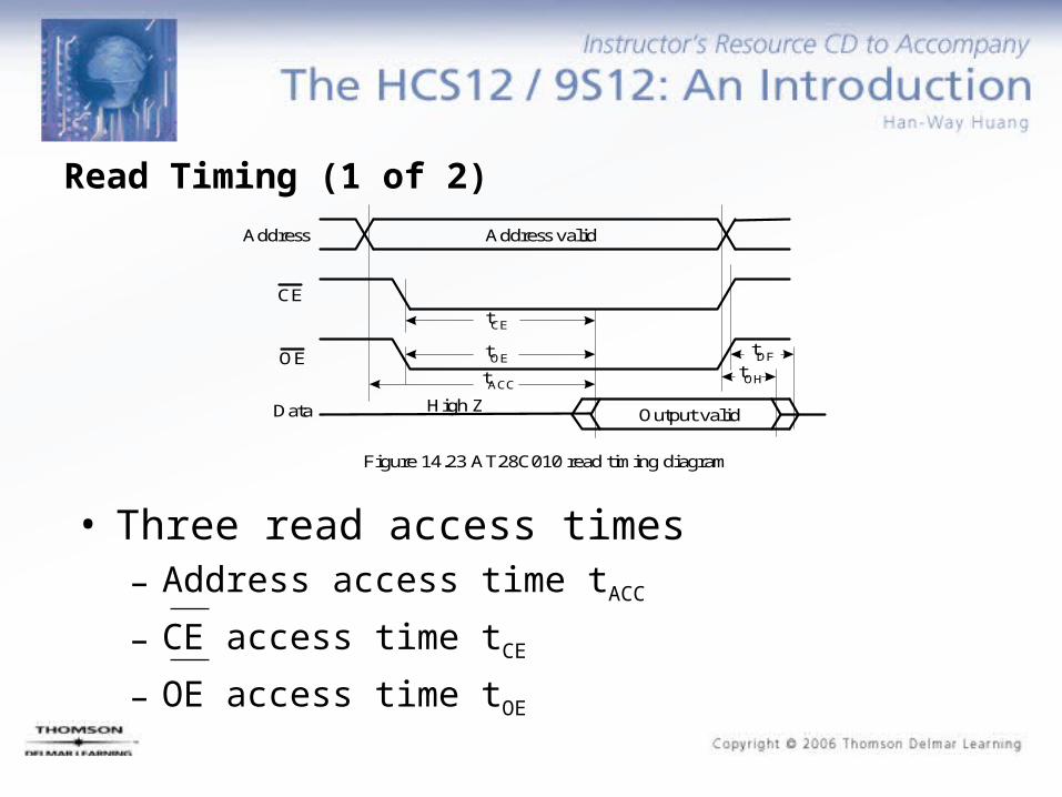
Figure 14.23 AT28C010 read timing diagram
CE
OE
Read Timing (1 of 2)
• Three read access times– Address access time tACC
– CE access time tCE
– OE access time tOE

Symbol Parameter
tACCtCE
(1)
tOE(2)
tDF(3)(4)
tDH
Address to output delayCE to output delayOE to output delayOE to output floatOutput hold from OE, CE, oraddress, which occurred first
AT28C010-12 AT28C010-15unit
Min. Min.Max. Max.
nsnsnsnsns
Table 14.11 AT28C010 Read characteristics
Max.AT28C010-20
Min.
000
1201205050
000
1501505555
000
2002005555
Notes.1. CE may be delayed up to tACC - tCE after the address transition without impact on tACC.2. OE may be delayed up to tCE - tOE after the falling edge of CE without impact on tCE or by tACC - tOE after an address change without impact on tACC.3. tDF is specified from OE or CE whichever occurs first (CL = 5pF).4. This parameter is characterized and is not 100% tested.
Read Timing (2 of 2)

OE
Address
CE
WE
Data In
tDStDH
tWP
tAH
tOES
tAS
tCS
tOEH
tCH
(a) WE controlled write timing waveform
OE
Address
WE
CE
Data In
(b) CE controlled write timing waveform
tWP
tAH
tOES
tAS
tCS
tDS tDH
tCH
tOEH
Figure 14.40 AT28C010 Write cycle timing waveform
Write Timing (1 of 3)
• WE-control• CE-control
A0-A12
Data
tAS tAH
Valid Addr.
Valid Data
Byte 1 Byte 2 Byte 3Byte 0 Byte 126 Byte 127
tWC
tBLCtWPHtWP
tDS tDH
Figure 14.41 AT28C010 Page mode write waveform
OE
CE
WE
Write Timing (2 of 3)
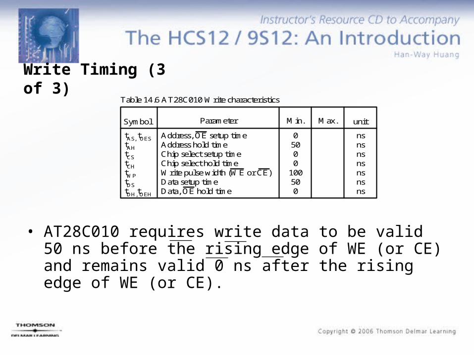
Symbol Parameter
tAS, tOEStAHtCStCHtWPtDStDH,tOEH
Address, OE setup timeAddress hold timeChip select setup timeChip select hold timeWrite pulse width (WE or CE)Data setup timeData, OE hold time
unitMin. Max.
nsnsnsnsnsnsns
Table 14.6 AT28C010 Write characteristics
05000
100500
Write Timing (3 of 3)
• AT28C010 requires write data to be valid 50 ns before the rising edge of WE (or CE) and remains valid 0 ns after the rising edge of WE (or CE).

Example of External Memory Expansion for the HCS12
• Design a demo board with 256 KB of 16-bit SRAM memory module and 256 KB of 16-bit EEPROM memory system.
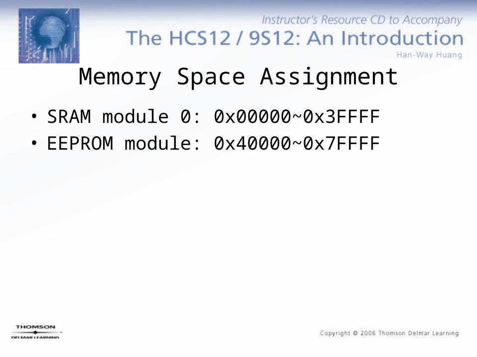
Memory Space Assignment
• SRAM module 0: 0x00000~0x3FFFF• EEPROM module: 0x40000~0x7FFFF
Address Latch (1 of 2)
• Two 74ABT16373s (shown in Figure 14.43) are used to latch address signals A15~A0.
• 74ABT16373 requires the input setup time to be 1 ns and hold time to be 0.5 ns.
• 74ABT16373 has the typical propagation delays of 4.4 ns.• At 25 MHz E clock, address signals A15-A0 are valid 20.5 ns after
the start of a bus cycle:A<15:0> valid time = the delay of the rise edge of ECS from the start of ECLK + propagation delay of 74ABT1637
= 16 ns + 4.4 ns = 20.4 ns

1 482 47
46454443424140393837363534333231302928272625
3456789101112131415161718192021222324
1OE1Q01Q1
GND1Q21Q3
VCC1Q41Q5
GND
GND
GND
GND
GND
GND
GND
VCC VCC
VCC
1Q61Q72Q02Q1
2Q22Q3
2Q42Q5
2Q62Q72OE 2E
2D72D6
2D52D4
2D32D2
2D12D01D71D6
1D51D4
1D31D2
1D11D01E
Figure 14.42 Pin assignment of 74ABT16373B
74ABT16373B
1E
2E
ECS
A15/D15~A0/D0
A15~A0
1OE
2OE
Figure 14.43 Address latch circuit for the HCS12
Address Latch (2 of 2)
Address Decoder Design
• In this example, the 1-MB memory space is divided into 4 256-KB modules.
• The address signals XA19 and XA18 should be used as decoder inputs.
• Either a 3-to-8 decoder (e.g. 74F138) or a dual 2-to-4 decoder (e.g., 74F139) can be used as the decoder.
• The chip select signal equations are as follows:– SRAM_CS = !(!XA19 * !XA18 * ECS)– EEPROM_CS = !(!XA19 * XA18 * ECS)
Write Control Signals
• The MCU may want to write into an individual byte rather than a whole word when writing to the external SRAM.
• Let WE1 and WE2 be the write enable signals for the upper and lower bytes.
• WE1 = !(LSTRB * !A0 * !R/W + LSTRB * !R/W) = !(!A0 * !R/W)
• WE2 = !(LSTRB * A0 * !R/W + LSTRB * A0 * !R/W) = !(A0 + !R/W)

Output Enable Signal
OE = !R/W

A0
W
ECS
XA18
XA19
SRAM_CS
EEPROM_CS
WE1
WE2
GAL16V8
Figure 14.45 Address decoder and write-enable signals generating circuit
OE
Address Decoder and Control Signal Generating Circuit
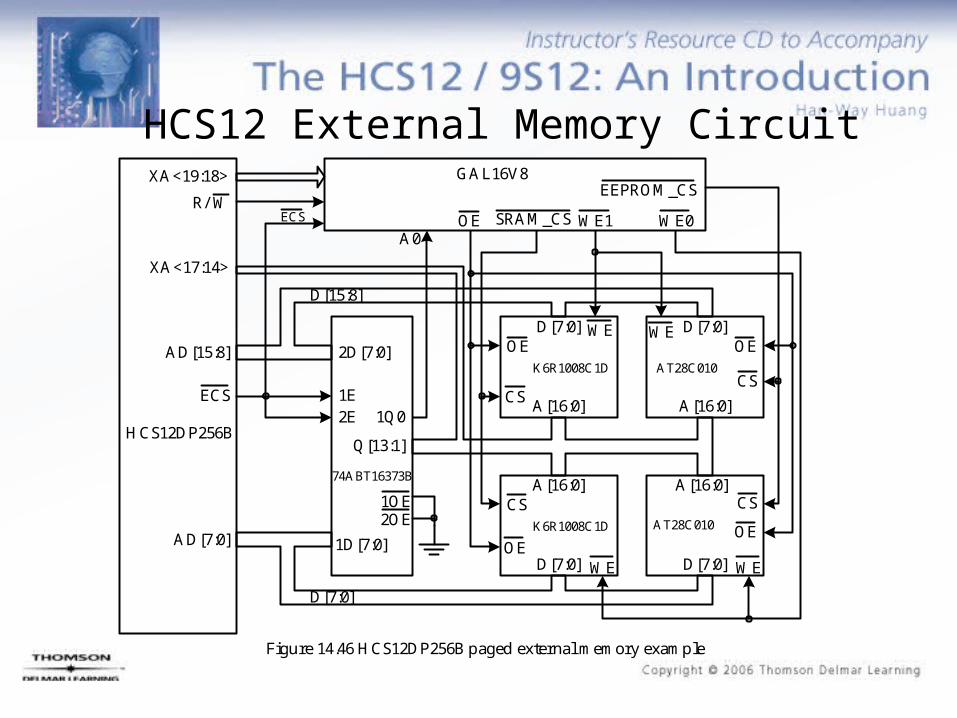
• All chip select signals, all write enable signals, and the output enable signal can be generated by using a single programmable logic device such as the Lattice Semiconductor GAL16V8.
• The resultant control circuit is shown.
XA<17:14>
XA<19:18>
AD[15:8]
AD[7:0]
ECS 1E2E
Q[13:1]
1Q0
D[15:8]
D[7:0]
D[7:0] D[7:0]
D[7:0] D[7:0]
A0
R/ W
2D[7:0]
1D[7:0]
ECS
GAL16V8
OE
OE
OEOE
OE
WE1SRAM_CS
CS
CS
WE
EEPROM_CS
CS
CS
WE0
WE
WE WE
A[16:0] A[16:0]
A[16:0] A[16:0]
K6R1008C1D
K6R1008C1D AT28C010
AT28C010
74ABT16373B
HCS12DP256B
Figure 14.46 HCS12DP256B paged external memory example
1OE2OE
HCS12 External Memory Circuit

• Example 14.16 For the circuit shown in Figure 14.46, can the SRAM be accessed without stretching the E clock? Assume the E clock is 25 MHz.
• Solution:

Address Timing
• The address inputs A12-A0 to the memory chip become valid 20.5 ns after the start of a bus cycle.
• The address inputs A16-A13 become valid 6 ns after the start of a bus cycle.
• The complete address inputs A16-A0 become valid 20.5 ns after the start of a bus cycle.
Chip Select Signals Timing
• The ECS becomes valid 16 ns after the start of a bus cycle.
• XA19-XA18 are valid 6 ns after the start of a bus cycle.• The GAL16V8 has a propagation delay of 3.5 ns.• The chip select signals SRAM_CS and EEPROM_CS
become valid 19.5 ns after the start of a bus cycle.• The HCS12 drives XA18-XA19, and ECS for 2 ns after a
bus cycle, these two chip select signals stay valid 5.5 ns after the end of a bus cycle.
Write Enable Signals Timing
• WE1 and WE0 are a function of A0 and R/W signals and A0 is valid later than R./W.
• WE1 and WE0 will be valid 24 ns (20.5ns + 3.5ns) after the start of a bus cycle.
• These two signals will stay valid 5.5 ns after the end of a bus cycle.
Output Enable Signal Timing
• The OE signal is the complement of the R/W signal.
• R/W is valid 7 ns after start of a bus cycle.• The OE signal will be valid 10.5 ns after start of
a bus cycle and remain valid 5.5 ns after the end of a bus cycle.
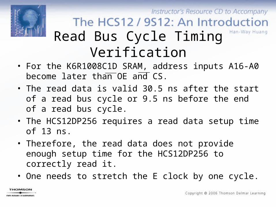
Read Bus Cycle Timing Verification
• For the K6R1008C1D SRAM, address inputs A16-A0 become later than OE and CS.
• The read data is valid 30.5 ns after the start of a read bus cycle or 9.5 ns before the end of a read bus cycle.
• The HCS12DP256 requires a read data setup time of 13 ns.
• Therefore, the read data does not provide enough setup time for the HCS12DP256 to correctly read it.
• One needs to stretch the E clock by one cycle.

Write Cycle Timing Verification (1 of 2)
• The address inputs to the K6R1008C1D stay valid until the new address is latched in the next address cycle.
• Therefore, address inputs A16-A0 stay valid for a whole E clock period (40 ns at 25 MHz) and satisfy the requirement 10 ns (tWC).
• The WE1 and WE0 signals have a low pulse width of 21.5 ns (40 ns – 24 ns + 5.5 ns) and satisfy the SRAM requirement.
• The HCS12 drives the write data 27 ns after the start of a write cycle (or 13 ns before the end of a write cycle).

Write Cycle Timing Verification (2 of 2)
• Both the WE and CS signals stay valid until 5.5 ns after the end of a write cycle. This provides 18.5 ns of write data set up time and satisfies the requirement.
• The HCS12 drives write data for 2 ns after the end of a write cycle but the WE signal goes high 5.5 ns after the end of a write cycle.
• The HCS12 does not provide enough write data hold time (at least 0 ns).
• However, the HCS12 does not drive the address/data bus for 8 ns after the end of a write cycle.
• The capacitance on the PCB can keep the data valid and satisfy the write data hold requirement.
• The E clock needs not be stretched for the write cycle.

• Example 14.17 Provide an analytical proof that the capacitance of the printed circuit board can hold the data voltage for enough time to satisfy the data hold time requirement of the SRAM.
• Solution: – The voltage of the data input to the K5R1008C1D is degraded by the
following leakage currents:• Input current to the HCS12 data pin (typically on the order of 2.5 A)• Input current into the EEPROM chips (on the order of 10 A).• Other leakage paths (assume to be as large as 10 A).
• The capacitance of the PCB is estimated to be 20 pF per foot.• Let C, I, V, and t be the capacitance of the PCB of one data line,
total leakage current, voltage change due to leakage current, and the time it takes for the voltage to degrade by V.
t CV I = 20 pF 2.5 V 22.5 A 2.2 s• This number shows that the capacitance on the PCB can keep the
voltage valid long enough to satisfy the write data hold time requirement.

• Example 14.18 For the circuit shown in Figure 14.46, can the EEPROM be accessed without stretching the E clock assuming that the 120 ns access time version of the AT28C010 is used? If not, how many cycles should the E clock be stretched?
• Solution: – According to Example 14.16, address signals A16-A0 become valid 30.5 ns after
the start of a bus cycle.– The read data from AT28C010 become valid 150.5 ns after the start of a read
cycle.– For the 25 MHz HCS12, this is 110.5 ns too late from the end of a read bus
cycle.– If we stretch the E clock by the maximum 3 E cycles, then the data becomes
valid 9.5 ns before the end of the read cycle. This is still not early enough.– The only solution is to slow down the clock frequency. If we reduce the clock
frequency to 24 MHz, then the read data setup time is increased to 16.17 ns and satisfies the requirement.
– Without stretching the E clock, the HCS12 provides 17.5 ns write data setup time which is shorter than the required 50 ns.
– After stretching E clock by 3 cycles, it would satisfy this requirement and also provides enough pulse width for the WE1 and WE0 signals (at least 100 ns).
movb #01,EBICTL ; enable E clock to stretchmovb #$0D,MISC ; stretch E by 3 periods
movb #$0C,PEAR ; enable ECLK, R/W, and LSTRB; disable ; NOACC, IPIPE1 and IPIPE0
• Example 14.19 Write an instruction sequence to configure the EBICTL and MISC registers to stretch the external bus cycles by three E clock periods.
• Solution: – The following instruction sequence will do the
requirement setting:
• When adding external memory, the signals R/W, ECLK, LSTRB need to be enabled.
• The following instruction will enable these signals properly:


