Page 1
83
CHAPTER 3
EPITAXIAL GROWTH AND CHARACTERIZATION OF
ALUMINUM NITRIDE GROWN BY METAL ORGANIC
CHEMICAL VAPOR DEPOSITION
3.1 INTRODUCTION
Deep ultra violet (DUV) light emitting diodes (LEDs) and laser
diodes (LDs) are revolutionizing the field of optoelectronics with applications
in high density optical data storage, biomedicine, water and air purification
(Schubert et al 2005, Taniyasu et al 2006 and Khan et al 2005). Aluminum
nitride (AlN) and aluminum gallium nitride (AlGaN) are the potential
materials to realize the DUV light emission due to their direct wide band gaps
(Khan et al 2008a). Also, AlN possesses high thermal conductivity (3.2 W
cm-1 K-1) and high breakdown voltage (12 MV cm-1) essential for high-power
and high temperature electronic devices (Mishra et al 2002a and Eastman et al
2002]. In addition, AlN has minimal lattice mismatch to high Al content
AlGaN layers and excellent UV light transparency (Kueller et al 2012) which
makes it a suitable buffer layer for DUV LED and LD device structures.
Generally, AlN has been grown heteroepitaxially on sapphire,
silicon carbide (SiC) and silicon (Si) substrates due to the lack of native
substrates resulting in high densities of threading dislocations (TDs) (Bai et al
2006). Indeed, growth of AlN has many challenges, which have been
addressed by adopting exceptional approaches in the growth conditions. For
example, (i) high sticking coefficient of aluminum (Al) restricting the
Page 2
84
migration of Al adatoms has been wiped out by growing AlN at higher
growth temperatures above 1200 °C (Ohba et al 2000) and by using pulsed
growth or migration-enhanced metalorganic chemical vapor deposition
(MEMOCVD) system (Zhang et al 2002). (ii) Unwanted parasitic reactions
between Al and ammonia (NH3) have been reduced by allowing high flow of
hydrogen (H2) carrier gas in to the reactor with low reactor pressure (Reentila
et al 2008). (iii) Cracking of AlN layers due to thermal expansion mismatch
between AlN and sapphire substrate has been encountered by multi-growth
mode modification (Okada et al 2007a). (iv) Three dimensional (3D) island
growth of AlN with poor surface morphology due to the polarity changes of
AlN and its dependency with the pre-treatment of sapphire substrate has been
studied by Paduano et al (2004). It has been found that AlN with Al polarity
exhibits smoother surface and AlN with mixed polarity (Al and nitrogen) has
rougher surface morphology (Paduano et al 2004a, Jasinski et al 2003 and
Kumagai et al 2007a). Nevertheless, pre-flow of precursors before the
deposition of nucleation layers [NLs] (Reentila et al 2008), growth
temperature of AlN-NLs (Balaji et al 2012a), thickness of NLs, density and
size of nucleation islands (NIs) have remarkable effect on the quality of AlN
layers (Wang et al 2006, Fan et al 2010a and Wang et al 2012).
The effect of initial growth stages such as pre-flow of trimethyl
aluminum (TMAl) and ammonia (NH3) prior to NL growth, direct deposition
of NL, influence of NL growth temperatures and the role of NIs coalescence
on the surface morphology and structural quality of AlN layers have been
discussed.
3.2 METAL ORGANIC CHEMICAL VAPOR DEPOSITION
SYSTEM
Manasevit et al has proposed a new approach to the growth of III-V
semiconductors by using metal organic precursors (1969).
Page 4
86
This approach began the rapid development of metal organic
chemical vapor deposition (MOCVD) technique in the 1970s. Earlier
difficulties in achieving high purity and abrupt interfaces have now been
faded out. Today, MOCVD has become the most promising technique for
heteroepitaxial growth and for its ability of mass production with uniform
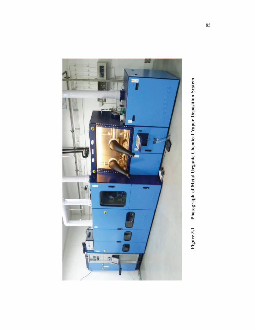
quality. In this chapter, AlN layers grown using Aixtron 200/4 RF-S MOCVD
sytem has been analyzed. The MOCVD system has been housed in the class
10,000 clean room. MOCVD system consists of electrical cabinet with server
computer, gas mixing cabinet with metal organic sources, reactor cabinet,
glove box, process pump, radio frequency generator, scrubber, ammonia and
silane gas cabinets, exhaust pipes and purging and carrier gases. Figure 3.1
shows the MOCVD system.
3.2.1 Electrical Cabinet
All the components in the MOCVD system have been interfaced
with the safety control system (SCS) located in the electronic cabinet. These
components can be operated by the server computer (mounted in the cabinet)
through the AIXACT software, by loading the recipes. In addition SCS
prevents the entire system and switches the system to a safe state if any
dangerous situation occurs. The SCS monitors all signals, valve positions,
sensors and analog limit values. It operates stand-alone and is superior to the
server computer.
Eurotherm temperature controller in the cabinet controls the reactor
temperature. Reactor pressure has been controlled by the pressure control unit
(PCU). The PCU consists of ‘MKS’ controller and two ‘Eurotherm’
controllers for run and vent line respectively. The MKS controller controls the
position of throttle valve and in turn the reactor pressure.
Page 5
87
Figure 3.2 Important components and electrical cabinet of MOCVD
a – Monitoring and status LED panel; b – Eurotherm temperature
controller and differential pressure controllers; c – MKS reactor
pressure controller; d – Luxtron touch screen monitor for in-situ
reflectance and process temperature; e – server computer;
f – Electrical cabinet.
Page 6
88
The run and vent lines of the metal organic and hydrides precursors
are controlled by active pressure balancing. To avoid a decrease of pressure
when switching a gas source from the vent line to the run line, a differential
pressure measurement has been carried out between both the lines. Figure 3.2
depicts the LEDs panel, controllers and computer located in the electrical
cabinet.
In the Figure 3.2(a) set of LEDs at the front side of cabinet, display
alarms and system status. The LEDs under the monitoring portion indicates
the major alarm. To run the system, all alarm had to be removed. The color of
LEDs disclose the state of MOCVD system. The green color of LEDs
indicates ‘no active alarms’, red color indicates ‘active alarm’ and orange
color indicates ‘no active alarm’ but needs to reset the SCS. The LEDs under
the status portion of the panel reveals only the status of precursors, water and
pressure valves. If the valves are open then the corresponding LED glows in
green color and the LED glows in red color for closed valves. On the back
side of the cabinet, the main switch has been situated. It should be turned off
for any electrical component related testing or maintenance.
3.2.2 Safety Measures
Growth of III-nitride materials in MOCVD involves pyrophoric
metal organic (MO) sources, highly inflammable hydrogen gas (carrier gas),
toxic silane and ammonia gas. Small amount of leakage in any of these gases
will lead to an unsafe situation. Hence, all the gas lines in the MOCVD
system, such as run and vent line of metal organics and hydrides, entire gas
mixing cabinet, reactor cabinet, silane and ammonia gas cabinet have been
periodically checked by helium gas leak detector. In addition to this, leak test
has been performed while installing the new sources (MO and Hydrides) and
replacing the empty bottles.
Page 7
89
Figure 3.3 depicts the helium leak detector. There are two modes
for leak detection (blowing and sniffing mode). In the former mode helium
gas is blown, all over the evacuated region of the MOCVD system and in the
latter mode the helium gas is fed in to the region of interest. Then the detector
checks for the helium gas by sniffing all over the region. The blowing mode is
the suitable method for checking the cabinets and the source lines of MOCVD
system, in which the gas lines have been connected with the detector by
suitable bellows, O-ring and with K-flanges. After that, the connected regions
are evacuated by the leak detector gradually.
Figure 3.3 Helium gas leak detector for checking the MO lines, gas
mixing cabinet and reactor cabinet
Page 8
90
Once the region has been evacuated to the level of 10-3 bar, helium
gas is blown externally all over the evacuated region. In the case of leakage,
the detector indicates the leak by giving a continuos buzzer in both the modes.
In order to handle process gases (MO, hydrides and hydrogen), in
an emergency or accident, MOCVD system has been equipped with exhaust
pipe lines, emergency off (red color) and process stop (yellow color) buttons.
Figure 3.4 shows the emergency and process stop buttons located in the glove
box, electrical and gas mixing cabinets. Pressing the EMERGENCY-OFF
button in the dangerous situation terminates the power supply of MOCVD
system. Pressing the PROCESS-STOP button leads to the following steps
All gas lines are purged with nitrogen
Throttle valve is closed
All hydrogen and metal organic source valves are closed
Process heater is turned off
Running recipe is terminated
Figure 3.4 Emergency off and process stop buttons in MOCVD system
Page 9
91
Figure 3.5 (a) Drager gas sensors controlling unit, (b) Gas sensor
display and (c) Hydrogen and ammonia sensors mounted on
the wall and exhaust pipes
Page 10
92
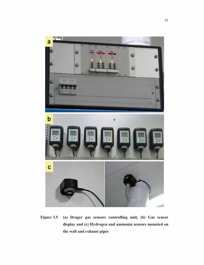
In addition to these safety buttons, ammonia, silane and hydrogen
gas sensors are mounted on the walls, exhaust pipes and gas cylinder rooms.
The gas sensors are highly sensitive. It can deduct the gases in the order of
parts per million (ppm). Alarm levels of all the gases are 30 ppm. If any gas
level exceeds this value, the Drager sensor controller automatically triggers
the alarm and aborts the recipe. Figure 3.5 depicts the Drager sensors
controlling unit, display of the gas values, ammonia and hydrogen sensor
mounted on the clean room and exhaust pipes.
3.2.3 Gas Mixing Cabinet
The gas mixing cabinet (GMC) consists of a gas pipe system, gas
purifiers, metal organic sources and control components like
Valves (manual, pneumatic 2/2, 3/2, 4/2, 5/2 valves)
Mass flow controllers (MFCs) for controlling the gas flows
Pressure controllers (PCs) for controlling the source pressures
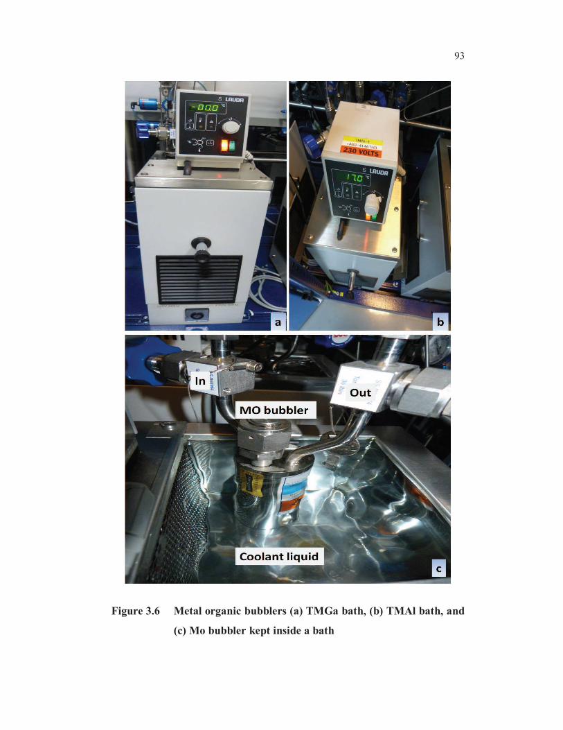
Figure 3.6 shows the baths with thermostat and MO bubbler. In the
front side of the GMC, four MO baths are located, two trimethyl gallium
(TMGa), one trimethyl aluminum (TMAl) and one bis-cyclopentadienyl
magnesium (Cp2Mg). On the rear side of the GMC, one trimethyl indium
(TMIn) and one triethyl gallium (TEGa) are situated. Hydrogen gas has been
used as the carrier gas in the front side of the MO bubblers. Cp2Mg is the
precursor of p-type dopant magnesium in III-nitrides. Silage is used as a
precursor for n-type doping in III-nitirdes.
Consequently, nitrogen gas has been used as the carrier gas for the
TMIn and TEGa MO bubblers. These precursors are used mainly for
InGaN/GaN based multi-quantum wells (MQWs) structures utilized in the
visible LED device structures.
Page 11
93
Figure 3.6 Metal organic bubblers (a) TMGa bath, (b) TMAl bath, and
(c) Mo bubbler kept inside a bath
Page 12
94
Normally, InGaN layers are grown in slightly lower growth
temperature (700 – 800 °C) for better indium incorporation than GaN layers
(~ 1000 °C). In the InGaN based MQWs, TEGa has been used as the
precursor of gallium, in order to grow the GaN layer in the same temperature
regime as that of InGaN. The temperature of precursor baths have been set
corresponding to the vapor pressure of MO bubblers. TMGa has higher vapor
pressure than all the MOs. Thus the bath temperature of TMGa was set at 0.0
°C. On the other hand, all the other precursor’s bath temperature were set at
17.0 °C due to their lower vapor pressure. To maintain the set temperature in
the bubbler, coolant liquid has been used. In the MO bubbler, the inlet line
and out let line are distinguished by the height. The inlet line height of the
bubbler is a bit smaller than the outlet line.
Figure 3.7(a) depicts the mass flow controllers (MFCs), pressure
controllers (PCs), pneumatic and manual valves, interface between the
controller components and the server computer. Figure 3.7(b) reveals the run,
vent and purge gas lines presented inside the GMC. There are three run lines.
They are used to lead the process gas from the sources to the reactor chamber.
Hydride run line leads the ammonia gas to the reactor. MO1 run-line,
comprises TMGa, TMAl and Cp2Mg precursor in the front side of the GMC.
Those precursors are fed in to the reactor cabinet by hydrogen carrier gas.
MO2 run-line consists of TMIn and TEGa. Nitrogen carrier gas leads these
precursors to the reactor cabinet. Figure 3.8 shows the block diagram of MO1
and MO2 lines. For each run-line, there is a vent-line. They bypass the reactor
chamber and lead the process gases into the vacuum system. Switching the
process gas between the run and vent line has been done by a 5/2-way valve,
in which two states are possible
Page 13
95
Figure 3.7 Gas lines in MOCVD system (a) mass flow controllers
(MFCs), pressure controllers (PCs) and valves. (b) Run,
vent and purge lines
Page 14
96
If the 5/2-way valve is open, the process gas flows through the
run-line into the reactor. No process gas flows in the vent-line.
If the 5/2-way valve is closed, the process gas flows through
the vent-line and skips the reactor. Only the carrier gas flows
in the run-line.
Figure 3.8 Block diagram of MO1, MO2 and hydride sources lines to
the reactor cabinet
To avoid pressure compensation reactions during the switching
processes between run and vent lines, the pressure in the run/vent lines and in
the reactor chamber will be held at the same level. The mass flow controllers
control the process gas flow. The effective functioning of flow controllers
needs three bar pressure of nitrogen/hydrogen gas. In addition, GMC gas has
several purging lines for the reactor components.
Page 15
97
Figure 3.9 Hydrogen, nitrogen and ammonia gas purifiers present in
the rear side of gas mixing cabinet
Figure 3.9 shows the gas purifiers for hydrogen, nitrogen and
ammonia. Gas contaminants cause process variability and poor quality of
material. The purity of the gases are inevitable for the quality of epitaxial
layers. These gas purifiers use high surface area adsorbents to remove oxygen
and carbon impurities to less than one part per billion (ppb). Impurities are
bonded to the surface of the reactive media through chemisorption
Page 16
98
processes. The high surface area structure of the media helps provide a large
lifetime, dependent on the inlet gas impurity levels and average flow rate. The
purifying material is a nickel mixture for hydrogen and nitrogen gases.
Manganese resinate for ammonia gas. These materials are regenerable. The
dew point of hydrogen and nitrogen are -110 and -125 °C respectively. This
value indicates the gases are of high purity.
The entire MOCVD system is equipped with liquid sensors, shown
in Figure 3.10. These liquid sensors are connected to the SCS. If a sensor
detects liquid (cooling agent from a thermostat bath), the SCS automatically
triggers the alarm. When a liquid spilt on the liquid sensor, it leads to the
connectivity between two parallel contacts that activate the ‘waterleak’ alarm
in the monitoring panel. To remove the alarm, water leak has to be arrested
and the liquid sensor needs to be free from liquid.
Figure 3.10 Liquid sensors placed all over the MOCVD system
3.2.4 Reactor Cabinet
The reactor cabinet consists of a horizontal reactor in the stainless
steel housing, wafer transfer system, susceptor, quartz liner, RF inductor,
Page 17
99
Double O-Ring (DOR) system and in-situ reflectometer. Figure 3.11 depicts
the reactor cabinet and the important components. On the back side of the
reactor, cooling water system has been located.
Figure 3.11 Reactor housing and components in the reactor cabinet
Page 18
100
There are two gas lines for purging and rotation of susceptor. Light
pipe, liner and view ports are connected with purge lines. Both nitrogen and
hydrogen are used as purge gases. The susceptor rotation has been done by
gases using a gas foil rotation technique. Speed of the susceptor rotation can
be controlled by controlling the gas flow. The reactor has three view ports, the
rotation of susceptor can be seen through the front view port, In-situ laser
reflectometer was mounted on the top view port exactly above the susceptor
and the third viewport was located at the back side of the reactor. Figure 3.12
shows the reactor components present inside the stainless steel housing.
Separation plate, ceiling plate and the liner are made up of quartz.
The separation plate (see Figure 3.12 a) placed inside the reactor makes sure
that the incoming precursors from the MO run line and the hydride run line
are not mixed until they reach the susceptor region. The liner (see Figure 3.12
b) encases the susceptor holder and forms the real process chamber. The
ceiling plate is placed on the liner. During the process the deposition of AlN
and its related alloys occur on substrate and on the liner walls and ceiling
plate. Ceiling plate can be easily removed and it has to be cleaned often to
avoid the falling of particles on the substrate during the growth. On the other
hand, this set-up provides seldom cleaning of liner.
Substrate is loaded into the reactor and unloaded from the reactor
using the transfer sytem (see Figure 3.12 c) through the reactor gate. Once
the substrate is loaded on the susceptor, the transfer system is moved inside
the reactor. Then the reactor gate is locked by three pneumatic clamps.The
reactor gate has DOR system. It consists of inner and the outer (two) O-rings.
The intermediate volume is pumped continuously to ensure reliable and
controllable sealing. Figure 3.12 (d) shows the DOR sealing surface between
the transfer system and the reactor gate.
Page 19
101
Figure 3.12 (a) Separation plate and RF inductor (b) ceiling plate and
liner (c) wafer transfer sytem from glove box in to reactor
(d) Double O-Ring assembly at the reactor gate
Page 20
102
Growth of AlN and its related alloys require higher temperature
above 1200 °C. The susceptor is coated with tantalum carbide (TaC) material
to withstand higher temperature (~ 1400 °C) . Figure 3.13 depicts the picture
of the liner (taken out from the reactor), and the susceptor disks. Susceptor
comprises of two disks. It has rotation disk at the top and a static disk at the
bottom. The bottom disk has three holes for the gases to pass through. The top
disk is mounted on the bottom disk through a centre axle pin. During the gas
foil rotation, top disk slightly floats and revolves around the axle pin and in
turn substrate loaded on the top disk of the susceptor rotates. The rotation of
the susbtrate can be seen through the front view port, provided the liner walls
are free from coating.
3.2.4.1 Radio frequency generator
The Radio Frequency (RF) generator delivers RF power to a work
piece (susceptor) via an inductor or coil at its output. There are two modes of
operations available in the RF generator. They are the internal and remote
mode. In the internal mode the generator functions independently. All the
commands necessary for the operation of the generator are produced
internally. In the remote mode, the generator is integrated into and controlled
by a higher order control system. All necessary commands for the operation
of the generator are passed through the digital interfaces and shall be operated
through recipe. The RF Generator is constructed of two parts: The power
supply unit (19" sheet metal housing) and the oscillator (Aluminium diecast
housing and aluminium sheet metal housing). The power supply unit and the
oscillator are water cooled. In the MOCVD system, the RF oscillator and
inductor altogether called as exciter is located in the reactor cabinet. The
power supply unit known as RF generator is located separately from the
MOCVD system. The power supply unit and oscillator are connected to each
other through a supply cable and a control cable.
Page 21
103
Figure 3.13 (a) Quartz liner, (b) static bottom disk of susceptor with axle
pin, (c) top surface of rotation disk and (d) bottom surface
of rotation disk
Page 22
104
The exciter generates the RF signal. It produces a sinusoidal,
alternating voltage from the DC source voltage of the intermediate circuit.
The frequency of this alternating voltage is determined by the oscillator
circuit and it is the working frequency. The oscillator circuit consists of an
inductor and one or more capacitors. The transfer of RF power onto the work
piece is carried out via an inductor. The inductor is dependent on the work
piece and is matched to the frequency. The current consumption of the RF
generator is determined by the loss in the oscillator circuit and the load. The
monitoring electronics monitor the exciter for surge voltage, water
malfunctions, auxiliary voltage and the working frequency. The monitoring
electronics also transfers the work data of the exciter to the control electronics
in the power supply unit. Figure 3.14 discloses the RF generator and the
oscillator.
Figure 3.14 RF generator and RF oscillator of the MOCVD system
Page 23
105
3.2.4.2 In-situ reflectometer
One of the important components in the reactor cabinet is Epitune
III In-situ reflectometer placed above the top view port of the reactor (see
Figure 3.11). Epitune III is an optical system for temperature and reflection
measurements on wafers. The key features of Epitune III are
In-situ measurement of the wafer temperature
In-situ measurement of the light reflection on a wafer
Graphical analysis of the temperature and reflection of
measurement
Control of the reactor temperature during the process
Measurement of growth rate and thickness
Epitune III consists of temperature and reflection measuring unit,
lightpipe and detector for temperature measurements at the bottom of the
susceptor and Epitune III controller (see Figure 3.2 d). The optical measuring
unit measures the temperature and reflection values using the laser
wavelength source of 635 nm and also by an LED source of 880 nm. Laser
source at 635 nm is mostly used to obtain the reflectance and wafer
temperature information. At the same time, the temperature is measured at the
bottom of the susceptor through a light pipe. It is connected with a detector
which measure the radiation from the susceptor. Both the optical measuring
unit and light pipe are controlled by Epitune III controller. The controller
converts the measurement signals of the measuring units (raw data) to the
temperature and the reflection values. These values are displayed on the
touchscreen and made available to the AIXACT server for further graphical
analysis.
Page 24
106
Optical temperature measurement
The optical temperature measurement is based on the thermal
radiation that every body emits at a temperature above absolute zero. If the
emissivity of the measured object is known, the measured radiation energy
may be used to calculate the body’s temperature. The calculation is based on
Planck’s law of black body radiation. If the measurement is performed at one
specific wavelength, the radiated energy depends only on the temperatue of
the body
( , ) = x a1
-5
ea2T-1
(3.1)
where
a1 = 2hc2 and a2 = hc/k, E – Radiated energy, – Wavelength,
T – Temperature, – Emissivity, h – Planck’s constant and c – Speed of light
Reflection measurement
The measuring unit emits a light ray normal to the wafer surface
and measures the reflected radiation. This provides information about the
properties of the grown layer. Figure 3.15 shows the behaviour of incident
and reflected radiation from the gas to layer and susbtrate
The measurement of the growth rate and the layer thickness is
based on the principle of interference of monochromatic light. At the interface
of materials with different refractive indices, light rays are transmitted as well
as reflected. The resulting reflected intensity as a function of time is a
characteristic fingerprint of the layer. If the refractive indices of substrate.
layer and the gas in the reactor are known, the growth rate and the layer
thickness can be calculated from the reflection measurements.
Page 25
107
Figure 3.15 Incident and reflected radiation with respect to the
refractive indices
n1 – refractive index of the susbstrate; n2 – refractive index of
the layer; nG – refractive index of the gas;
Figure 3.16 shows the typical curve of the reflected intensity as a
function of time. The crest and the trough in the curve are caused by the
interference of the incident and the reflected radiation. T is the oscillation
time. The following formula can be used to determine the growth rate the
layer
= (3.2)
= (3.3)
Page 26
108
where
d – Thickness of the layer which has grown during the time T
T – Oscillation time
– Wavelength of the light source (635 nm)
n – Refractive index of the layer
r – Growth rate of the layer
Figure 3.16 Reflectance intensity versus time
In addition to these components, throttle valve and water cooling
system are situated at the rear side of the reactor cabinet. The pressure gauge
mounted near the reactor measures the pressure in the reactor and forwards
the measured pressure to the MKS pressure control unit (see Figure 3.2 (c)).
MKS controller controls the position of the throttle/butterfly valve in order to
Page 27
109
adjust pressure in the reactor according to the set point. Figure 3.17 shows the
throttle valve.
Figure 3.17 Throttle valve in the reactor cabinet
There are two separate water lines for the RF generator and the
reactor cabinet. Figure 3.18 depicts the cooling water system. RF generator
requires water flow rate of 21 liters/minute (+ or – 2). The reactor cabinet in
the MOCVD system needs 6 bar of the inlet water pressure for cooling system
and the maximum tolerable outlet water pressure is 2.5 bar. Drop and surge in
the water pressures triggers alarms and in turn aborts the process. Routine
checking of water lines are mandatory before the start of growth. There are
separate flow meters with flow limiter for reactor, flanges, RF oscillator, coil
or inductor and glove box water lines. If necessary the water flow can be
changed using manual valves for the standard flow rate. The inlet pressure
can be adjustable with the hand wheel and a water filter is located in the inlet
line to remove the dust particles. There is a provision to clean the filter by
means of back washing through the drain hose. This is a quick cleaning
process and there is no need for removing the filters.
Page 28
110
Figure 3.18 Cooling water system at the rear side of reactor cabinet
3.2.5 Glove Box
The glove box contains pure nitrogen atmosphere. It protects the
reactor from contaminations during loading/unloading the wafer through
transfer system and during maintenance. Two gloves are integrated with the
glove box for both the right and left hand to access the components such as
load lock chamber, wafer transfer system, vacuum tweezers and wand inside
the glove box. Substrates are transported into the glove box via the load lock.
The load lock chamber comprises of two doors: The outer door is used to load
and unload the substrates. The substrates for the growth is kept in the load
lock chamber through the outer door. Then the outer door of load lock
chamber is closed. Load lock chamber is purged with nitrogen gas followed
by evacuation. This cycle is repeated for three times in order to terminate
Page 29
111
oxygen and moisture entering into the glove box from the clean room. After
purging the load lock chamber, the inner door is opened through the gloves.
The inner door is used to transfer substrates between load lock chamber and
glove box. Figure 3.19 shows the load lock chamber, vacuum tweezers and
vacuum wand.
Figure 3.19 Load lock chamber, vacuum tweezers and vacuum wand in
the glove box
Page 30
112
To load and unload the substrate onto the susceptor, vacuum
tweezers is used. Vacuum tweezers handle the substrate only at the bottom. It
avoids the tweezers mark on the substrate’s surface completely. Vacuum
wand is a tool to take out the susceptor’s rotation disk from the axle. Both
vacuum tweezers and wand are operated with a pedal switch.
3.2.6 Process Pump and Scrubber
Process pump is used for evacuating the reactor up to 1 millibar.
This pump is connected with the reactor pressure control unit (see Figure 3.2
c) via the throttle valve. The process pump is an oil pump and it is purged
with nitrogen gas. The pump uses special white oil, which is normally clear
and transparent. If the oil darkens, it should be changed. The oil level can be
seen from the front side of the pump. The oil level of the pump should be
checked before the start-up. If necessary the oil should be topped up. The
process pump can pump condensable gases and vapours, provided that the gas
ballast valve is open and the pump has attained its operating temperature.
Proper operation of the pump is ensured in the ambient temperature range
between 12 to 40 °C.
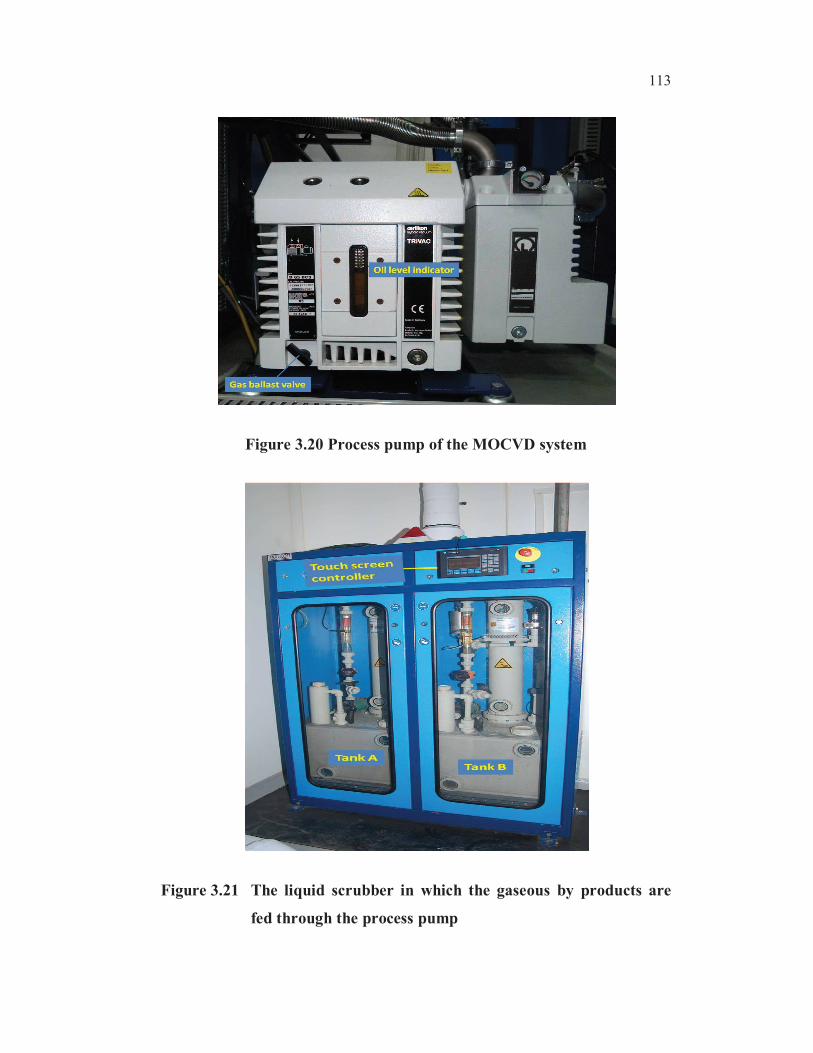
A stainless steel pipe connects the process pump and the scrubber.
The scrubber has two tanks and the tanks are filled with the cleansing
solution. The cleansing solution is a mixture of sulphuric acid and deionized
water. The gaseous by products are fed into the liquid scrubber. There, the
gases are detoxified. The scrubber has a touch screen controller. The
controller alerts when the solution level is low and if there are other problems
while pumping. The pH value of the solution is maintained at 5. The
cleansing solution should be replaced, if there is any sign of crystallization.
Switching on and off shall be done in the touch screen controller. Figure 3.20
and 3.21 depict the Leybold process pump and scrubber.
Page 31
113
Figure 3.20 Process pump of the MOCVD system
Figure 3.21 The liquid scrubber in which the gaseous by products are
fed through the process pump
Page 32
114
3.2.7 Ammonia and Silane Gas Cabinet
Figure 3.22 shows the ammonia, nitrogen and silane cabinet.
Ammonia is the precursor for nitrogen and silane is the precursor for silicon
(n-type dopant of III-nitrides). Ammonia cabinet has the provision of loading
two cylinders at a time. If one cylinder is at service, another cylinder is in
standby mode. If the service cylinder is empty during the growth, the
ammonia will be delivered by the standby cylinder without any interruption,
by means of an automatic change over valve. Since the nitrogen gas generated
from liquid nitrogen is being used, the dry nitrogen gas cabinet has not been
put in use.
Figure 3.22 Ammonia, nitrogen and silane gas cabinets
Page 33
115
3.2.8 Process Technology of MOCVD
Chemical vapor deposition is a common method to deposit thin
films. In a CVD process, volatile compounds are transported into the reactor
chamber via the gas phase. There the precursors are decomposed on a hot
substrate by thermal energy. The following reaction takes place step by step.
Figure 3.23 displays the CVD reaction steps
1 Transport of the reagents in the gas phase to the substrate, by
carrier gas
2 Diffusion of the molecules through the phase interface
gas/boundary layer
3 Adsorption on the substrate surface
4 Migration of the molecules to the crystallization zones
5 Chemical decomposition
6 Desorption of the by-products and diffusion and convection
out from the boundary layer
7 Transport of the by-products out from the reactor
Figure 3.23 Chemical vapour deposition reaction steps A – Gas phase;
B– Boundary layer; C – Substrate;
Page 34
116
3.3 EXPERIMENTAL PROCEDURE
Trimethylaluminum (TMAl) and ammonia (NH3) were used as
precursors for aluminum (Al) and nitrogen (N) respectively. Hydrogen was
used as the carrier gas. 2 c-plane sapphire substrate was loaded on the
susceptor and the surface of substrate was thermally cleaned at 1150 °C for 10
minutes in H2 ambient. Initially, three AlN layers were grown on nucleation
layers (NLs) deposited at 850 °C with a V/III ratio of 1024. Thickness of NLs
was around 30 nm. Only the pre-flow conditions prior to the growth of NLs at
850 °C were modified to optimize the initial growth condition. In the first
sample, the NL was grown directly after the thermal cleaning of the sapphire.
For the second sample, TMAl was fed in to the reactor for 30 seconds prior to
the NL growth called as alumination was carried out. In the third sample, pre-
flow of NH3 (nitridation) for 2 minutes was done before the NL growth. All
the AlN samples with thickness of about 2 m, were grown at 1300 °C with a
V/III ratio of 512 and, after the recrystallization of nucleation layers at
1250 °C. The nucleation layer growth was carried out between 850 and
1250 °C as explained below. Structural quality and surface morphology of
these AlN layers were investigated by high resolution x-ray diffraction (HR-
XRD) and atomic force microscopy (AFM) respectively.
The growth temperature of direct NLs grown beneath the high
temperature AlN layers was varied as 950 °C, 1050 °C, 1150 °C and 1250 °C
without altering other growth parameters such as recrystallization temperature
(Tr) of AlN-NLs (Tr ~1250 °C), growth temperature (Tg) of AlN layers (Tg ~
1300 °C), V/III ratios of AlN-NLs (1024) and AlN layers (512). The AlN
layers deposited on direct NLs grown at different temperatures were
characterized using HR-XRD, AFM and Raman spectroscopy. Further, to
understand the effect of NLs on the quality of AlN layers, three NLs growth
temperature were selected. NLs were deposited at the selected temperatures of
Page 35
117
950, 1050 and 1150 °C on sapphire substrates and subsequent
recrystallization was performed at 1250 °C for 2 minutes. The surface
morphology of recrystallized NLs and coalescence of NIs were assessed by
AFM.
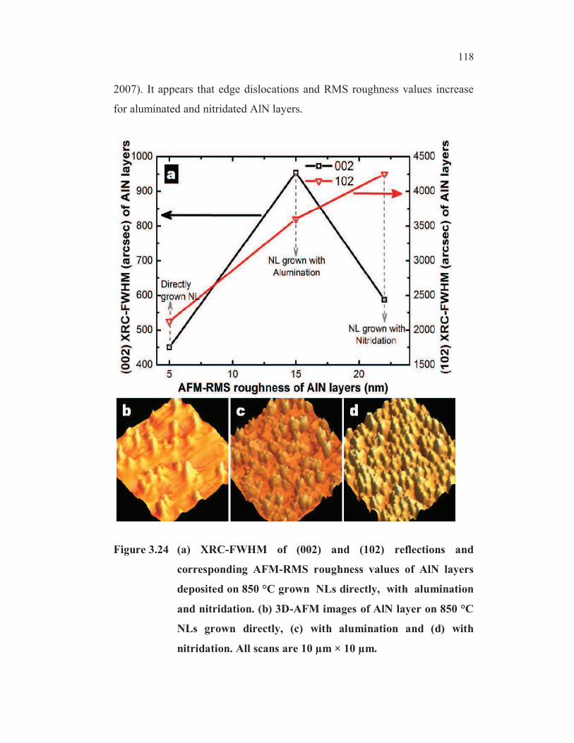
3.4 RESULTS AND DISCUSSION
3.4.1 Effect of Initial Growth Stages
Structural quality and surface morphology of 2 m thick AlN layers
grown on NLs (directly, with alumination and nitridation) deposited at 850 °C
have been presented in Figure 3.24. The x-ray rocking curve (XRC) full width
at half maximum (FWHM) values of (002) and (102) reflections and
corresponding AFM root mean square (RMS) roughness values were shown
in Figure 3.24 (a). The three dimensional (3D) AFM images of AlN layer
grown on direct NL, with alumination and with nitridation have been depicted
in Figure 3.24 (b), (c) and (d) respectively. The symmetric (002) and
asymmetric (102) peaks are related to the screw and edge threading
dislocations (Srikant et al 1997 and Heinke et al 2000). Screw and edge
threading dislocations have been found to originate from the tilt and twist of
the AlN-NIs with respect to the substrate (Fini et al 1998 and Chierchia et al
2003).
Figure 3.24 (a) reveals that the FWHM of (002) and (102)
reflections of the AlN layer on direct NL is as low as 450 and 2124 arcsec
compared with aluminated and nitridated AlN layers. Thus, the broadening of
(002) FWHM to 954 arcsec in the aluminated AlN layer indicates that the pre-
flow of TMAl prior to the NL increases the tilt of NIs perpendicular to the
surface normal. Higher (102) FWHM of 4248 arcsec in the nitridated AlN
layer shows the larger twist of NIs around the surface normal (Taniyasu et al
Page 36
118
2007). It appears that edge dislocations and RMS roughness values increase
for aluminated and nitridated AlN layers.
Figure 3.24 (a) XRC-FWHM of (002) and (102) reflections and
corresponding AFM-RMS roughness values of AlN layers
deposited on 850 °C grown NLs directly, with alumination
and nitridation. (b) 3D-AFM images of AlN layer on 850 °C
NLs grown directly, (c) with alumination and (d) with
nitridation. All scans are 10 µm × 10 µm.
Page 37
119
RMS roughness values of AlN layer grown on direct NL, with
alumination and with nitridation have been estimated from the AFM images
of scan area 10 µm × 10 µm as 5, 15 and 22 nm from Figure 3.24 (b), (c) and
(d) respectively. Both islands and flat surfaces have been observed on the AlN
layers grown with direct NL and aluminated NL. However the number of
islands has been noted to be lesser in AlN layer having direct NL. Observance
of flat surface is totally annihilated in the AlN layer grown with nitridated NL
(Figure 3.24 d), which could be the reason for higher surface roughness. On
the whole, alumination and nitridation of sapphire prior to the growth of NLs
leads to broader (002) and (102) FWHM of AlN layers respectively. Surface
morphology of nitridated AlN layer has been poor with prevailing island
growth. Direct deposition of NL on sapphire substrate revealed impact on the
quality of AlN layers. Thus, direct growth of NL has been adapted to improve
the quality of AlN layers.
3.4.2 Influence of Nucleation Layers Growth Temperature on the
Quality of AlN Layers
Figure 3.25 depicts the graph between reflectivity and growth time.
In-situ reflectance pattern of AlN layers grown with nucleation layers
deposited at 850 °C, 950 °C and 1050 °C shown in Figure 3.25 (a), (b) and (c)
respectively. In Figure 3.25 region ‘1’ represents the reflectance peak of AlN
nucleation layer and region ‘2’ represents the start of high temperature AlN
growth. Figure 3.25(a) reveals the gradual decrease in the reflectance
oscillation amplitudes. It indicates the surface of the AlN is not smooth. In
Figure 3.25 (b) the amplitudes of AlN layer reflectance oscillation is stable,
that shows the smoothness of AlN layer surface. Figure 3.25 (c) discloses AlN
layer surface is very rough, the amplitude of reflectance peak has been
drastically reduced.
Page 38
120
From the in-situ reflectance graph, it has been found that the AlN
layer grown on 950 °C NL has the smooth surface morphology than AlN
layers with 850 and 1050 °C NL.
Figure 3.25 In-situ reflectance pattern of AlN layer versus growth time
during the growth in MOCVD. (a) AlN layer grown on NLs
deposited at 850 °C, (b) 950 °C and (c) 1050 °C
1 – Reflectance peak of AlN-nucleation layer (NL); 2 – High
temperature AlN layer deposition starts after the
recrystallization of NL;
Page 39
121
Figure 3.26 reveals AlN layers XRC-FWHM of (002) and (102)
reflections as the function of NL growth temperatures used for the AlN layers.
The FWHM of (002) reflections are 202, 214, 164 and 288 arcsec. On the
other hand, FWHM of (102) reflections are 900, 864, 1368 and 1404 arcsec
for the AlN layers deposited on the NLs grown at 950, 1050, 1150 and
1250 °C respectively.
Figure 3.26 AlN layers XRC-FWHM of (002) and (102) reflections as the
function of NL growth temperatures from 950 to 1250 °C
used for the AlN layers. ((002) and (102) FWHM of AlN
layer grown on 850 °C NL can be seen in Figure 3.24 a)
Page 40
122
Both the (002) and (102) FWHM values are found to decrease as
the NLs growth temperature of AlN layers increase from 850 °C (Figure 3.24
a) to 950 °C. This trend continues for the AlN layer grown on 1050 °C NL
with slight increment and decrement in the (002) and (102) FWHM values.
The lowest (002) FWHM value of 164 arcsec has been obtained for the AlN
layer with 1150 °C NL. At the same time, the (102) FWHM has been found to
be as high as to 1368 arcsec. In the case of AlN layer with 1250 °C NL, both
the symmetric and asymmetric peaks FWHM are found to be broader. This
might be partly explained by the thermal decomposition of c-plane sapphire
substrate occur above 1200 °C in the H2 ambient (Akiyama et al 2007a),
resulting in the deterioration of AlN layer. HR-XRD results elucidate the
enormous effect of NLs growth temperatures on the AlN layers and edge
dislocations are dominant in the AlN layers.
Threading dislocations and in-plane stress of AlN layers, originates
due to large lattice and thermal expansion mismatch between AlN and
sapphire substrate (Yim et al 1973) were estimated. Threading dislocations
(TDs) with screw components NS (screw + mixed type TDs) and edge
components NE (edge + mixed type TDs) have been calculated from the
Equations (3.4) and (3.5)
=( )
( ) (3.4)
=)
( )(3.5)
where,
bS = 4.982 Å and bE = 3.112 Å are the AlN Burger vector lengths of screw
components and edge components respectively (Dunn et al 1957).
Page 41
123
FWHM(002) and FWHM(102) have to be converted in radian for
calculation. In-plane stress has been calculated using the following
Equation:
)2(33
213
12110
c
ccc
a
aall (3.6)
where ‘a’ is the lattice constant of AlN layers, a0 = 3.112 Å is the lattice
constant of unstrained AlN and the elastic constants of AlN Cij are C11 = 410
GPa, C12 = 140 GPa, C13 = 100 GPa and C33 = 390 GPa (Deger et al 1998). In
which AlN lattice constant ‘a’ has been calculated using the equation:
2
2
2
22
2)(
3
41
c
l
a
khkh
dhkl (3.7)
Screw NS, edge NE components of threading dislocation densities
and in-plane stress of the AlN layers deposited on NLs grown at temperatures
that varied from 850 to 1250 °C have been tabulated in Table 3.1.
As can be seen from Table 3.1, screw dislocation densities of AlN
layer are decreased by an order from 4.3 × 108 cm-2 to 6 × 107 cm-2 as NL
growth temperature increases from 850 to 1150 °C. It is then increased to 1.7
× 108 cm-2 for 1250 °C NL. Edge dislocation densities of AlN layers also
decrease from 2.5 × 1010 cm-2 to 4.1 × 109 cm-2 when increasing NLs growth
temperature of AlN layers from 850 to 1050 °C and start to increase further
with increasing NLs growth temperature to 1150 °C and 1250 °C. Over all
threading dislocation density has been found to be minimum for the AlN
layers grown on 950 °C and 1050 °C NLs, and might be attributed to the
reduced tilt and twist of NIs at these temperatures.
Page 42
124
Table 3.1 Nucleation layers growth temperature, screw NS and edge
NE components of threading dislocation density and
In-plane stress of AlN layers
NL growth
temperature of
AlN layers (°C)
Threading dislocation density In-plane
stress
(GPa)
Screw (108 cm-2)
components NS
Edge (1010 cm-2)
components NE
850 4.3 2.5 -0.32
950 0.8 0.44 -0.91
1050 0.9 0.41 -0.82
1150 0.6 1.03 -1.05
1250 1.7 1.09 -1.18
Moreover, the calculated in-plane stress, ( ) shows that all the
AlN layers are in compressive strain, negative sign indicating the compressive
strain. The in-plane compressive strain has been found to increase with NL
growth temperatures, excluding a small drop in the stress value for AlN layer
grown on 1050 °C NL. XRD results enunciate that 950 °C and 1050 °C grown
NLs are the optimal NL growth temperature to reduce the structural defects in
the AlN layer.
Figure 3.27 shows three dimensional AFM images of AlN layer in
the scan area of 10 µm × 10 µm. Figure 3.27 (a-d) reveal the images of AlN
layers grown with NLs from 950 - 1250 °C. AlN surface morphology
becomes rougher on increasing the NLs growth temperature. It is worth
noticing the clear steps and smooth surface of AlN layer grown on 950 °C NL
in Figure 3.27 (a). Step flow and emerging island like structure are seen in
Figure 3.27 (b) corresponding to the AlN layer with 1050 °C NL. In Figure
3.27 (c) and (d) granular or island structures are observed for the AlN layers
Page 43
125
grown on 1150 and 1250 °C NLs. Appearance of layer by layer (Frank-Van
der Merwe) and layer-island (Stranski-Krastanov) growth modes pronounces
the influence of NLs growth temperature used for AlN layers. This could be
also due to the differences in the growth rate (Kumagai et al 2007) between
AlN-NLs (5 nm/min) and AlN layers (35 nm/min). RMS roughness value
measured in Figure 3.27 (a-d) are found to be 1, 13, 42 and 32 nm for AlN
layers grown on 950, 1050, 1150 and 1250 °C NLs. The higher surface
roughness is obvious due to the absence of step growth and prevalence of
island growth on increasing the NLs growth temperature. Specular surface
morphology with RMS roughness of 1 nm indicates high crystalline quality
(Kaeding et al 2004) of AlN layer grown on 950 °C NLs. The AFM results
are well accordance with in-situ recflectance pattern (see Figure 3.24). In-situ
reflectance, structural quality and surface morphology of AlN layers are noted
to favour the 950 °C grown NL than the1050 °C NL.
Raman spectra has been recorded for AlN layers deposited on NLs
grown at 850, 950 , 1050 , 1150 and 1250 °C using laser excitation source of
532 nm at room temperature in a backscattering geometry. Raman spectral
resolution is 0.9 cm-1. In backscattering geometry, the allowed Raman phonon
modes for (002) oriented AlN are E2 modes and the A1 (LO) mode (Kuball
2001 a). Figure 3.28 shows the Raman spectra of AlN layers. A1 (TO) and E1
(TO) phonon modes are usually forbidden in the backscattering geometry.
Dotted circle and circles in the Figure 3.28 indicates the weak signals of A1
(TO) and E1 (TO) phonon modes, respectively. It may be due to the presence
of misaligned 3D-islands or grains (Deng et al 2005 and Harima 2002),
for AlN with partial and complete granular surface as can be seen in the AlN
layers deposited on NLs grown at 850 (Figure 3.24 b), 1050 (Figure 3.27 b),
1150 (Figure 3.27 c) and 1250 °C (Figure 3.27 d).
Page 44
126
Figure 3.27 3D-AFM images of AlN layers deposited on NLs grown at
(a) 950 °C, (b) 1050 °C, (c) 1150 °C and (d) 1250 °C. AlN
layer grown on 850 °C NL was shown in Figure 3.24(b).
All scans are 10 µm × 10 µm.
Page 45
127
Figure 3.28 Raman spectra of AlN layers deposited on NLs grown at
850-1250 °C. Dotted circle represents A1(TO) mode and
open circles show E1(TO) mode. The inset depicts observed
phonon modes of AlN layers from 600 to 900 cm-1
In the AlN layer grown on 950 °C NL, there are no distinct feature
of A1 (TO) and E1 (TO) phonon modes. Inset shows the Raman phonon modes
of AlN layers from 600 to 900 cm-1. The E2 (high) phonon mode is found to
be sensitive to in-plane strain. The E2 (high) phonon mode position of
Page 46
128
unstrained AlN layer is at 657 cm-1. Shift towards higher frequency side in the
E2 (high) phonon modes as 658.22, 657.5, 658.24, 658.26 and 659 cm-1 for
AlN layers with NLs grown at 850 – 1250 °C has been observed. It exhibits
that all the AlN layers are in compressive strain. The calculated in-plane
stress values using the equation (3.6) and the position of E2 (high) phonon
peaks ascertain the in-plane compressive strain of AlN layers. Raman spectra
show AlN layer with 950 °C NL is free from misaligned AlN grains.
Figure 3.29 UV-Visible transmission spectra of AlN layers
Figure 3.29 depicts UV transmission spectra of AlN layers as the
function of wavelength. AlN layer with 950 °C NL has the higher optical
transparency throughout the visible region of the spectrum and well into the
UV region. The transmission curve also has a sharp drop off at 200 nm
wavelength, which corresponds to the bandgap of AlN. Decrease in the
transparency for other AlN layers might be partially due to the surface
Page 47
129
morphology. The rough surfaces of AlN layer decrease the transmission due
to the reflection and scattering of light.
3.4.3 Investigation of Nucleation Layers
In this section, NLs have been examined to understand their role in
determining the quality of AlN layers. Figure 3.30 (a), (b) and (c) disclose
three dimensional AFM images of recrystallized (at 1200 °C for 2 minutes)
NLs grown at 950, 1050 and 1150 °C respectively.
Firstly, 3D-AlN islands nucleate on the sapphire surface and start to
coalesce during the recrystallization of NLs. The 3D-islands tend to tilt and
twist around each other in order to undergo coalescence. In this process,
screw dislocations are found to originate from the tilt of NIs, edge
dislocations arise at the island or grain boundaries due to the NIs twist. Most
of these dislocations propagate in the subsequent AlN growth. Uniform
coalescence of nucleation islands have pronounced effects in suppressing the
intrusion of threading dislocations and formation of specular surface with step
and terrace growth pattern in the AlN layers. The NL grown at 950 °C shown
in Figure 3.30 (a) is found to exhibit the uniformly coalesced NIs, which
could be attributed to the step and terrace growth of AlN layer (Figure 3.27 a).
Whereas uneven coalescence of NIs is observed in Figure 3.30 (b), 1050 °C
grown NL leads to the step flow and emerging island like structure of AlN
layers (Figure 3.27 b). In Figur 3.30 (c) harsh undulations of coalesced NIs
and inadequate surface coverage of NIs are seen in NL grown at 1150 °C, it
could be attributed to the very rough surface of AlN layer (Figure 3.27 c).
Page 48
130
Figure 3.30 3D-AFM images of recrystallized NLs grown at (a) 950 °C,
(b) 1050 °C and (c) 1150 °C. All scans are 1µm × 1µm
Page 49
131
NIs density, diameter, height and RMS roughness values are
presented in Table 3.2. The NIs densities have been in the order of 1010 cm-2
for all three recrystallized NLs. The variation in the NIs diameter and height
has been found to increase with NL growth temperatures. RMS roughness
also increases with NLs growth temperatures. Smaller NIs and very low
variations in the diameter and height of NIs aid to uniform coalescence in the
NL grown at 950 °C. Relatively higher NIs density, diameter, height and
variation in the size could be attributed to uneven coalescence in the NL
grown at 1050 °C. Low density and big size of NIs have been found essential
to obtain good surface morphology and structural quality (Datta et al 2004).
Table 3.2 NL growth temperature, nucleation island density,
diameter, height and AFM-RMS roughness values for the
nucleation layers grown at various temperature.
NL growth
Temperature
(°C)
NI
density
(1010
cm-2
)
NI
diameter
(nm)
NI
height
(nm)
AFM-RMS
roughness
(nm)
950 7 80-100 7-10 1.5
1050 9.6 40-300 4-13 3
1150 3 100-360 3-16 3.9
Despite this fact, lower NIs density and large size of NIs obtained
for the NLs grown at 1150 °C have failed to fulfill the anticipation. It might
have been due to insufficient coverage of NIs on the surface and high
variation in NIs height, which favours the non-uniform coalescence of NIs
with highly undulated surface. Consequently, surface roughness of the
recrystallized NLs has been found to increase with increasing NL growth
temperatures. It is worth noticing that coalescence of NIs play a vital role in
determining the structural quality and surface morphology of the AlN layer.
Page 50
132
Optical microscope images (not shown) confirmed that AlN layers
are free from cracks. Thermal expansion co-efficient differences (extrinsic
stress) between AlN and sapphire are found to cause cracks in the AlN layers.
However, in-plane compressive strain of AlN layers found from XRD and
Raman spectroscopy can also be attributed to the absence of cracks.
3.5 CONCLUSION
Direct deposition of AlN NL, effect of nucleation layer growth
temperatures, role of nucleation islands coalescence with respect to the
density, size and height have been investigated. The influence of NL
temperature in the aspect of producing evenly sized NIs and the uniformity in
the coalescence of NIs have been found as important growth parameters to
achieve the device quality AlN layers. Increasing the NL growth temperature
from 850 to 950 °C has been found to improve the quality of AlN layers.
Further increase in the NL growth temperature destructs the structural quality
and surface morphology due to the uneven coalescence of nucleation islands.