33
Chapter 3: Chapter 3: Sequential Logic Circuit Sequential Logic Circuit – – Shift Register - Shift Register - EKT 121 / 4 EKT 121 / 4 ELEKTRONIK DIGIT 1 ELEKTRONIK DIGIT 1
| Date post: | 13-Dec-2015 |
| Category: |
Documents |
| Upload: | amice-leonard |
| View: | 241 times |
| Download: | 2 times |
Chapter 3: Chapter 3: Sequential Logic Circuit Sequential Logic Circuit
– – Shift Register -Shift Register -
EKT 121 / 4EKT 121 / 4ELEKTRONIK DIGIT 1ELEKTRONIK DIGIT 1

© Copyright 2000 Indiana University Board of Trustees
Basic shift register function Serial in / serial out shift registers Serial in / parallel out shift registers Parallel in / serial out shift registers Parallel in / parallel out shift registers Bidirectional shift registers Shift register applications
3.2 Shift Register

© Copyright 2000 Indiana University Board of Trustees
Sequential Logic CircuitsSequential Logic Circuits
Combinational logic
Memory elements
Combinational outputs Memory outputs
Inputs
Sequential circuit = Combinational logic + Memory Elements
Current State of A sequential Circuit: Value stored in memory elements (value of state variables).
State transition: A change in the stored values in memory elements thus changing the sequential circuit from one state to another state.

© Copyright 2000 Indiana University Board of Trustees
A register is a memory device that can be used to store more than one-bit information
A register is usually realized as several flip-flops with common control signals that control the movement of data to and from the register
……….
RegistersRegisters

© Copyright 2000 Indiana University Board of Trustees
RegistersRegisters An n-bit register is a collection of n D
flip-flops with a common clock used to store n related bits.
D 1QCLR
Q
Q /1Q1D
D 2QCLR
Q
Q /2Q2D
D 3QCLR
Q
Q /3Q3D
D 4QCLR
Q
Q /4Q4D
CLK
/CLR
74LS175Example: 74LS175 4-bit register
CLKCLR
4Q4Q3Q3Q2Q2Q1Q1Q
74LS175
1D
2D
3D
4D

© Copyright 2000 Indiana University Board of Trustees
Shift RegistersShift Registers
Multi-bit register that moves stored data bits left/right ( 1 bit position per clock cycle)
0 1 1 1 LSI
Q3 Q2 Q1 Q0
1 1 1 LSI
Q3 Q2 Q1 Q0
RSI 0 1 1 1
Q3 Q2 Q1 Q0
RSI 0 1 1
Q3 Q2 Q1 Q0
– Shift Right (or Shift Up) is towards MSB
– Shift Left is towards MSB

© Copyright 2000 Indiana University Board of Trustees
Basic Shift Register FunctionsBasic Shift Register Functions
Consist of an arrangement of flip-flops Important in applications involving
storage and transfer of data (data movement) in digital system
Used for storing and shifting data (1s and 0s) entered into it from an external source and possesses no characteristic internal sequence of states.
D flip-flops are use to store and move data

© Copyright 2000 Indiana University Board of Trustees
The flip-flop as a storage The flip-flop as a storage elementelement
When a 1 is on D, Q becomes a 1 at triggering edge of CLK or remains a 1 if already in the SET state
When a 0 is on D, Q becomes a 0 at triggering edge of CLK or remains a 0 if already in the RESET state
© Copyright 2000 Indiana University Board of Trustees
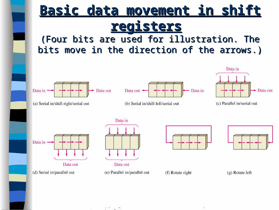
Basic data movement in shift Basic data movement in shift registersregisters
(Four bits are used for illustration. The bits move in (Four bits are used for illustration. The bits move in the direction of the arrows.)the direction of the arrows.)

© Copyright 2000 Indiana University Board of Trustees
Types of Shift RegisterTypes of Shift Register
1. Serial In / Serial Out Shift Registers (SISO)2. Serial In /Parallel Out Shift Registers (SIPO)3. Parallel In / Serial Out Shift Registers
(PISO)4. Parallel In / Parallel Out Shift Registers
(PIPO)

© Copyright 2000 Indiana University Board of Trustees
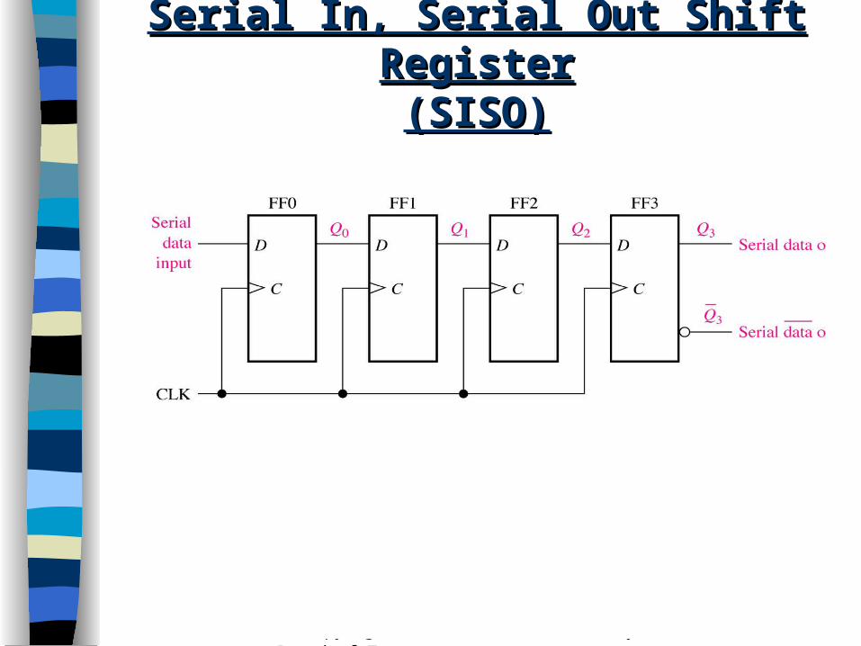
Serial In, Serial Out Shift Serial In, Serial Out Shift RegisterRegister(SISO)(SISO)
D Q
CLK
D Q
CLK
D Q
CLK
SERIN
CLOCK
SEROUT
For a n-bit SRG:Serial Out = Serial In delayed by n clock period
4-bit shift register example:serin: 1 0 1 1 0 0 1 1 1 0serout: - - - - 1 0 1 1 0 0clock:
SRG n>SI SO
© Copyright 2000 Indiana University Board of Trustees
Serial In, Serial Out Shift Serial In, Serial Out Shift RegisterRegister(SISO)(SISO)

© Copyright 2000 Indiana University Board of Trustees
Serial In, Serial Out Shift Serial In, Serial Out Shift RegisterRegister (SISO)(SISO)

© Copyright 2000 Indiana University Board of Trustees
Serial In, Serial Out Shift Serial In, Serial Out Shift RegisterRegister (SISO)(SISO)
© Copyright 2000 Indiana University Board of Trustees
Serial In, Serial Out Shift Serial In, Serial Out Shift RegisterRegister (SISO)(SISO)
© Copyright 2000 Indiana University Board of Trustees
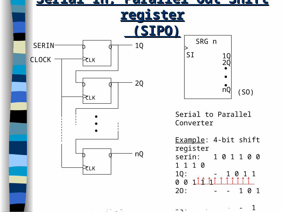
Serial In, Parallel Out Shift Serial In, Parallel Out Shift registerregister (SIPO)(SIPO)
D Q
CLK
D Q
CLK
D Q
CLK
SERIN
CLOCK
nQ
2Q
1Q
Serial to Parallel Converter
Example: 4-bit shift register serin: 1 0 1 1 0 0 1 1 1 01Q: - 1 0 1 1 0 0 1 1 12Q: - - 1 0 1 1 0 0 1 13Q: - - - 1 0 1 1 0 0 14Q: - - - - 1 0 1 1 0 0clock:
SRG n>SI 1Q
2Q
nQ (SO)

© Copyright 2000 Indiana University Board of Trustees
Serial In, Parallel Out Shift registerSerial In, Parallel Out Shift register (SIPO)(SIPO)
• Data bits entered serially (right-most bit first)
• Difference from SISO is the way data bits are taken
out of the register – in parallel.
• Output of each stage is available

© Copyright 2000 Indiana University Board of Trustees
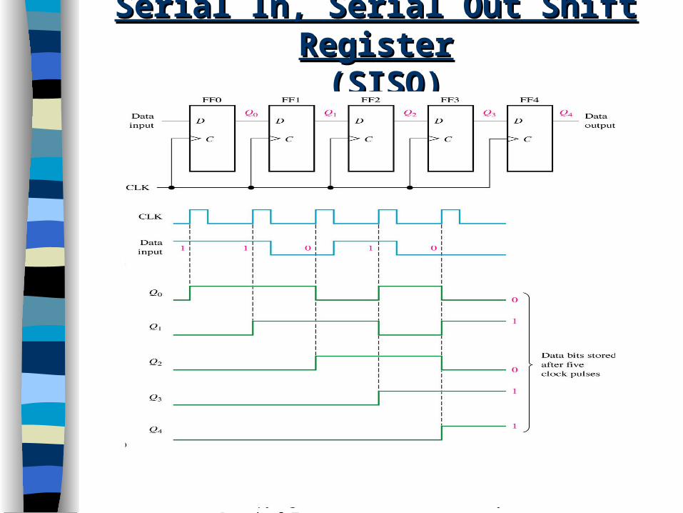
ExampleExample : :
The states of 4-bit register (SRG 4) for the data input The states of 4-bit register (SRG 4) for the data input and clocks waveforms. and clocks waveforms.
Assume the register initially contains all 1s
© Copyright 2000 Indiana University Board of Trustees
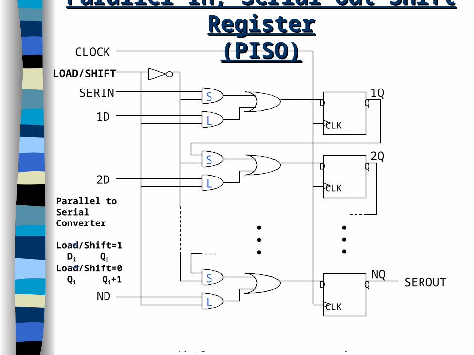
Parallel In, Serial Out Shift Parallel In, Serial Out Shift RegisterRegister(PISO)(PISO)
SERIN
CLOCK
D Q
CLK
D Q
CLK
D Q
CLK
SEROUT
LOAD/SHIFT
1D
2D
ND
S
L
S
L
S
L
1Q
2Q
NQ
Parallel to Serial Converter
Load/Shift=1 Di Qi
Load/Shift=0 Qi Qi+1

© Copyright 2000 Indiana University Board of Trustees
4-bit parallel in/serial out shift 4-bit parallel in/serial out shift registerregister(PISO)(PISO)

© Copyright 2000 Indiana University Board of Trustees
Parallel In, Parallel Out Shift Parallel In, Parallel Out Shift RegisterRegister(PIPO)(PIPO)
SERIN
CLOCK
D Q
CLK
D Q
CLK
D Q
CLK
LOAD/SHIFT
1D
2D
ND
1Q
2Q
NQ
S
L
S
L
S
L
General Purpose:Makes any kind of (left) shift register

© Copyright 2000 Indiana University Board of Trustees
Parallel In, Parallel Out Shift Parallel In, Parallel Out Shift Register (PIPO)Register (PIPO)
Immediately following simultaneous entry of all data bits,it appear on parallel output.

© Copyright 2000 Indiana University Board of Trustees
Bi-directional Shift RegistersBi-directional Shift Registers
Data can be shifted left Data can be shifted right A parallel load maybe possible 74HC194 is an bidirectional universal
shift register
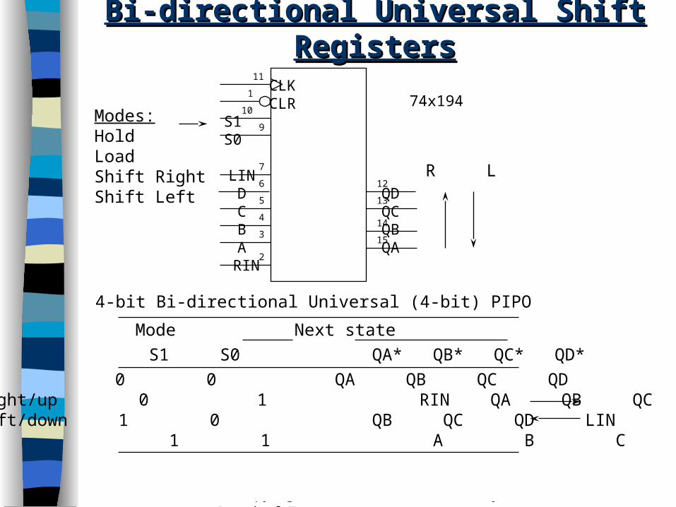
© Copyright 2000 Indiana University Board of Trustees
Bi-directional Universal Shift Bi-directional Universal Shift RegistersRegisters
4-bit Bi-directional Universal (4-bit) PIPO
CLK CLR S1 S0
LIN D QDC QCB QBA QARIN
11
1
10
9
7
6
4
5
3
2
12
13
14
15
74x194Modes:HoldLoadShift RightShift Left
R L
Mode Next state
Function S1 S0 QA* QB* QC* QD*
Hold 0 0 QA QB QC QDShift right/up 0 1 RIN QA QB QCShift left/down 1 0 QB QC QD LINLoad 1 1 A B C D

© Copyright 2000 Indiana University Board of Trustees
Four-bit Johnson countersFour-bit Johnson counters Serial output
connected back toserial input
The complement of the output (Q’) is fedback into
1st FF.

© Copyright 2000 Indiana University Board of Trustees
Five-bit Johnson countersFive-bit Johnson counters

© Copyright 2000 Indiana University Board of Trustees
A 10-bit ring counter A 10-bit ring counter Assume initial state : 1010000000

© Copyright 2000 Indiana University Board of Trustees
Shift Register ApplicationsShift Register Applications State Registers
– Shift registers are often used as the state register in a sequential device. Usually, the next state is determined by shifting right and inserting a primary input or output into the next position (i.e. a finite memory machine)
– Very effective for sequence detectors Serial Interconnection of Systems
– keep interconnection cost low with serial interconnect Bit Serial Operations
– Bit serial operations can be performed quickly through device iteration
– Iteration (a purely combinational approach) is expensive (in terms of # of transistors, chip area, power, etc).
– A sequential approach allows the reuse of combinational functional units throughout the multi-cycle operation

© Copyright 2000 Indiana University Board of Trustees
Shift Register Applications Shift Register Applications Example:Example: Serial Interconnection of Serial Interconnection of SystemsSystems
Serial DATAParallel-to-serial converter
Parallel Data from
A-to-D converter
Serial-to-parallel converter
Parallel Data to D-to-A converter
Control
Circuits
CLOCK
/SYNC
TransmitterControl
Circuits
Receiver
n nOne bit

© Copyright 2000 Indiana University Board of Trustees
Shift Register Applications Shift Register Applications Example:Example: 8-Bit Serial Adder8-Bit Serial Adder
...7 6 5 0>
x7 x6 x5 x0
...7 6 5 0>
y7 y6 y5 y0
...7 6 5 0>
FACout S
Cin A BD Q
CLK
CLR
CLK
CLEAR_Cz7 z6 z5 z0...
CTL Sequential Implementation of:Z[7..0] = X[7..0] + Y[7..0]
V
© Copyright 2000 Indiana University Board of Trustees
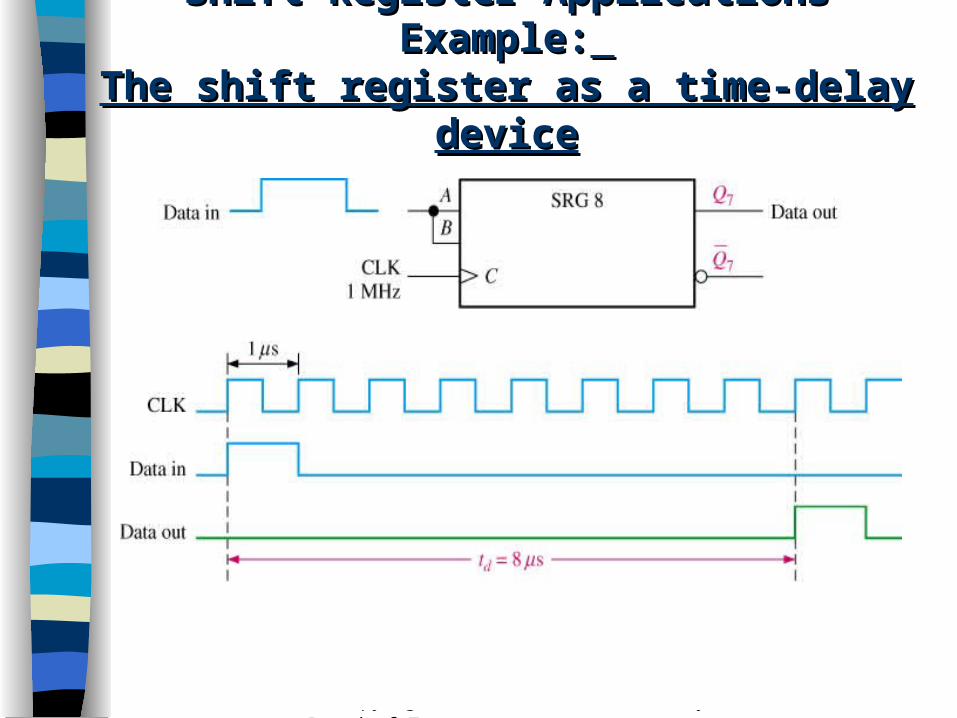
Shift Register Applications Shift Register Applications Example:Example:
The shift register as a time-delay The shift register as a time-delay devicedevice
© Copyright 2000 Indiana University Board of Trustees
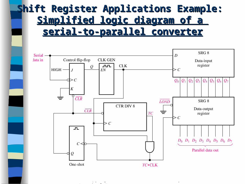
Shift Register Applications Example:Shift Register Applications Example: Simplified logic diagram of a Simplified logic diagram of a serial-to-parallel converterserial-to-parallel converter

© Copyright 2000 Indiana University Board of Trustees
Thank youThank you


