Page 1
59
CHAPTER IV
DESIGN AND ANALYSIS OF VARIOUS PWM TECHNIQUES FOR BUCK
BOOST CONVERTER
4.1 Conventional Method
A buck-boost converter circuit is a combination of the buck converter topology
and a boost converter topology in cascade. The output to input conversion ratio is also a
product of ratios in buck converter and the boost converter. The output voltage is
controlled by controlling the switch-duty cycle. The ratio of output voltage to input
voltage is given by [69]:
Where, VO and VIN are the output and input voltages, respectively. The term IO and
IIN is the output and input currents, respectively.
The term D is the duty ratio and it is defined as the ratio of the on time of the
switch to the total switching period. This shows the output voltage to be higher or lower
than the input voltage, based on the duty-ratio D [70].
4.1.1 Features and applications of buck boost converter
a) Features
1.Regulated Output with VIN Above, Below or Equal to VOUT.
2.2.7V to 15V Input Voltage Range.
3.2.5V to 14V Output Voltage Range.
4.2.5A Continuous Output Current: VIN ≥ 5V, VOUT = 5V, PWM Mode.
5.750 kHz Switching Frequency, Synchronize Between 300 kHz and 1.5 MHz
6.Output Current Monitor.
7.Internal N-Channel MOSFETs.
Page 2
60
8.Up to 95% Efficiency.
9.Selectable Burst Mode Operation, IQ = 50µA.
b) Applications
1. 3.3V or5V from1, 2 or3 Li-Ion, Backup Capacitor Stack [71].
2. RF Transmitters.
3. Hand Held Inventory Terminals.
4. 2V Synchronous Boost Converter.
5. LED Lighting with Current Regulation.
6. Multiple Power Input Systems.
7. 12V Lead Acid Battery to 12V.
Normal PWM technique is used. The Pulse Width Modulation (PWM) is a
technique which is considered by the generation of constant amplitude pulse by
modulating the pulse duration by modulating the duty cycle. An analog PWM control
requires the generation of both reference and carrier signals that are supply into the
comparator and based on some logical output, the final output is generated. The reference
signal is the desired signal output maybe sinusoidal or square wave, while the carrier
signal is either a saw tooth or triangular wave at a frequency much greater than the
reference [11].
There are two basic PWM techniques:
1. Single Pulse Width Modulation.
2. Multiple Pulse Width Modulation.
4.1.2 Single Pulse Width Modulation
In this modulation there is an only one output pulse per half cycle. The output is
changed by changeable width of the pulses. The gating signals are generated by
comparing a rectangular reference with a triangular reference. The frequency of the two
signals nearly equal.
Page 3
61
Fig. 4.1. Generation of Single PWM.
4.1.3 Multiple Pulse Width Modulation
In this modulation there are various numbers of output pulses per half cycle and all
pulses are of equal width. The gating signals are generated by comparing a rectangular
reference with triangular reference. The frequency of the reference signal sets the output
frequency (fo) and carrier frequency (fc). The variation of modulation index (MI) from 0
to 1 varies the pulse from 0 to π/p and the output voltage from 0 to Vs.
Fig.4.2 Generation of Multiple PWM.
Page 4
62
4.2 Proposed Converter
Proposed controller based Buck Boost converter is used, so that the voltage
produced efficiently. The controller constantly monitors the output voltage from the
Converters. Corresponding to the magnitude of the DC output from the rectifier, the
controller calculates and changes the width of the pulse given to the converted, to boost it
to the rated voltage of the Converter [12].
A Buck Boost Converter is a DC/DC regulator which provides an output voltage
that may be lesser than or greater than the input voltage. Hence, it is called “Buck-
Boost”. As the polarity of the output voltage is opposite to that of the input voltage, the
regulator is also known as an inverting regulator. Among all the topologies that are used
to Buck as well as Boost the voltage, Buck Boost converter has wider acceptance as it
provides a significant improvement in performance and efficiency by eliminating the
transition region between buck and boost mode.
Fig.4.3 Circuitof Buck-Boost Converter.
Page 5
63
4.2.1 Operation of Proposed Converter
Operation modes: The circuit operation can be divided into two modes:
Fig.4.4.Operation of Buck-Boost Mode 1.
Mode 1: Let D be the duty cycle and TS be the time period of the PWM signal. During
mode 1, the transistor is turned ON by the SPWM signal for a period (DTS) and the diode
is reverse biased. The input current flows through the inductor L and the transistor in
Mode 1 operation of Buck Boost Converter [9].
Mode 2: During the mode 2, the transistor is switched off by the PWM switching for the
period (1-DTS). The current, which was flowing through the inductor L during mode 1,
would now flow through the inductor L, capacitor C, Diode and the load. The energy is
stored in the inductor L would be transferred to the load and the inductor current would
fall until the transistor is switched on again in the next cycle. The amount of energy
stored in the inductor is determined by the duty cycle of the SPWM signal. The greater
the duty cycle, higher will be the energy stored in the inductor. If the duty cycle of
SPWM is below 50%, the circuit bucks the output voltage as the amount of energy stored
Page 6
64
is less and if it is above 50%, the output voltage will be boosted to the nominal battery
charging voltage.
Fig.4.5 Operation of Buck-Boost Mode 2.
The operation of Buck Boost converter may be in Continuous Current Mode
(CCM) or Discontinuous Current Mode (DCM) of operation depending on the Wind
Machine output. The converter should be operated in CCM to charge the battery which
depends on the value of the inductor and the load. Figure shows the mode 2 operation of
Buck Boost Converter [10].
4.2.2 DC Conversion Ratio
The DC conversion ratio M (D), is the ratio of output voltage to the input voltage
of the converter. Fig.4.6 shows the DC conversion ratio of the buck boost converter. The
curve is in the fourth quadrant as the output voltage polarity is opposite to that of the
input voltage [11]:
Where, VO-output voltage of the Buck Booster converter, Vin-input voltage.
Page 7
65
Fig 4.6 DC conversion ratio of the buck boost converter
For the duty cycle below 0.5, the DC conversion ratio is less than 1 indicating that
the converter will be operating in buck mode. Also for the duty cycle above 0.5, the ratio
rises exponentially indicating that the converter boosts the output voltage several times of
that of the input even if there is a small increase in the duty cycle. For normal operation
of the converter in the boost mode, the duty cycle should be only in the range from 0.58
to 0.67 [50].
4.3 Design of Buck Boost Converter Circuit
The integral part of Buck Boost converter design is to choose proper values of an
inductor (L) and Capacitor (C) because the output voltage depends on the L and C values.
The inductor and capacitor plays most important role in filtering the output from
the circuit to provide stiff DC. For the effective charging of the battery the Buck
Boost controller must operate in Continuous Current Mode (CCM) [51].
In order that the buck boost converter operates in CCM, optimum values of
inductor and capacitor must be chosen because if their values are higher than the cost
of winding, core size will also be high. If their values are low, high switching
frequency will need to obtain the same voltage level [48].
Page 8
66
This increases the cost of the switch involved. Therefore it is necessary to choose
optimum values of L and C.
For the Buck Boost converter operates within the safety limit, the components
used in it should have higher ratings than the values obtained in the design. Rated
charging voltage of the Buck Boost Converter circuit along with feedback terminals that
need to be connected with the ADC pins of the Microcontroller is shown in fig.4.7.
The MOSFET is switched based on the SPWM signal given to its gate. Thus, the
ON time and OFF time of the MOSFET is governed by the duty cycle of the PWM
signal. When the MOSFET is switched ON, the diode is in reverse bias and hence the
inductor stores the energy from the Wind machine. When the MOSFET is switched OFF,
the diode becomes forward bias and hence the inductor transfers the stored energy to the
capacitor. Higher the duty cycle, greater will be the energy stored in the inductor and
hence higher will be the output voltage [52].
Fig 4.7 Design of the buck boost converter.
Page 9
67
In most of the implementation, generation of the desired output voltage is
achieved by comparing the desired reference waveform (modulating signal) with a high
frequency triangular „carrier‟ wave. Depending on the signal voltage is larger or smaller
than the carrier waveform, either the positive or negative dc bus voltage is applied at the
output. Note that over the period of one triangle wave, the average voltage applied to the
load is proportional to the amplitude of the signal (assumed constant) during this period.
The root mean square value of the ac voltage waveform is still equal to the dc bus
voltage, and hence the total harmonic distortion is not affected by the PWM process [53].
The harmonic components are merely shifted into the higher frequency range and
are automatically filtered due to inductances in the ac system. When the modulating
signal is a sinusoid of amplitude Am, and the amplitude of the triangular carrier is Ac, the
ratio ` is known as the modulation index. Controlling the modulation index therefore
controls the amplitude of the applied output voltage with a sufficiently high carrier
frequency [56].
The high frequency components do not propagate significantly in ac network or
load due to the presence of the inductive elements. However, a higher carrier frequency
does result in a larger number of switching per cycle and hence in an increased power
loss. Typically switching frequencies in the 500 kHz range are considered adequate for
power systems applications. Also in three phase systems it is advisable to use all three
waveforms are symmetric [57].
The Sine Wave is used as a reference to generate PWM because the output
voltage is sine wave at 500 kHz supply, The DC source (VCD) is used as a carrier
signal. This DC source carrier signal is compared with a Sinusoidal reference signal. The
crossover points are used to determine the switching instants such that if V
reference is greater than V carrier then output is high otherwise output is low. The
Page 10
68
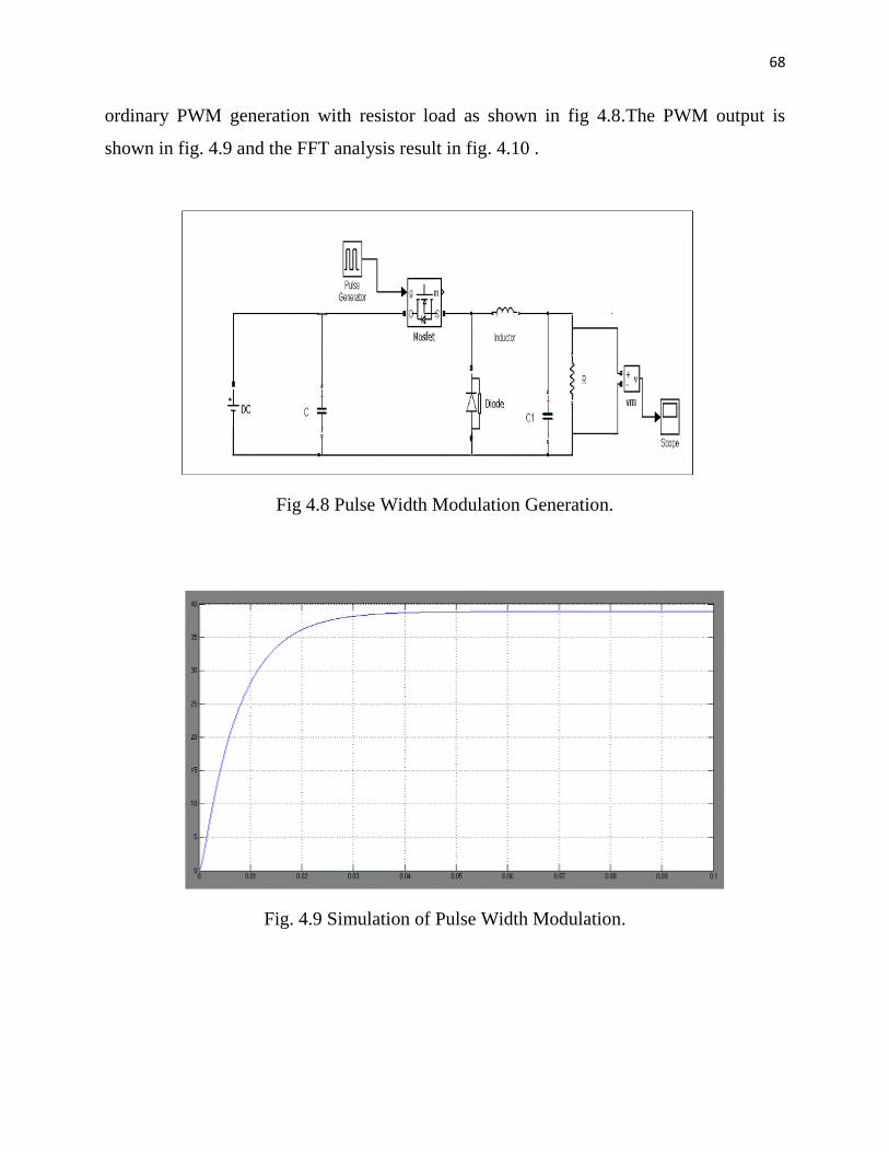
ordinary PWM generation with resistor load as shown in fig 4.8.The PWM output is
shown in fig. 4.9 and the FFT analysis result in fig. 4.10 .
Fig 4.8 Pulse Width Modulation Generation.
Fig. 4.9 Simulation of Pulse Width Modulation.
Page 11
69
Fig.4.10 FFT analysis of existing PWM.
4.4 Delay PWM Generators
The delay PWM is one of most utilized methods of Pulse Width Modulation
Techniques by which it can be produced by using a simple logic circuit in order to get an
output in a very simple manner, the delay PWM is works based on the block diagram
given in the figure. The ordinary PWM generation with resistor load as shown in fig 4.11.
Page 12
70
Fig 4.11 Proposed Pulse Width Modulation Generations.
In some situations it can be useful to vary the phase between two square waves.
Here, two D-flip-flops „A‟ and „B‟ convert the PWM signal into a square wave in the
standard manner. However, D-flip-flop 'A' is clocked by the rising edge of a Pulse Width
Modulated (PWM) signal, whereas D-flip flop 'B' is clocked by the falling edge, a pulse
from a reference clock starts a cycle and after a certain delay.
Designed to match the propagation delay experienced through the multiplexer, sets
the PWM output to high. The reference pulse propagates through the delay line and when
it reaches the output selected by the multiplexer its value is used to set the PWM output
to low. The total delay through the delay line is calculated to be equal to the reference
clock period [49].
Page 13
71
Fig 4.12 Delay based Pulse Width Modulation Generation.
Fig.4.13 Simulation of Delay Pulse Width Modulation.
Page 14
72
4.5 Generation of Sinusoidal Pulse Width Modulation Using FPGA
With the widespread use of digital techniques in instrumentation and
communications systems, a digitally-controlled method of generating multiple
frequencies from a reference frequency source has evolved called Direct Digital
Synthesis (DDS). The basic architecture is shown in Figure 4.14.
In this simplified model, a stable clock drives a programmable read-only-memory
(PROM) which stores one or more integral number of cycles of a sine wave (or other
arbitrary waveform, for that matter). As the address counter steps through each memory
location, the corresponding digital amplitude of the signal at each location drives a DAC
which in turn generates the analog output signal [23].
Fig.4.14 Block diagram of generation of Sinusoidal PWM Using FPGA.
.
Direct Digital Frequency Synthesizer
Sine Wave Generation
Comparator
MSG
S/g
Carrier
S/g
(CLK)
SPWM
O/P
Page 15
73
Fig. 4.15 Synthesis result of generation of SPWM for Area utilization.
Page 16
74
Fig. 4.16 Synthesis result of generation of SPWM for Power consumption.
Page 17
75
Fig. 4.17 Simulation result of generation of SPWM.
Page 18
76
Fig. 4.18 Synthesis result of generation of SPWM for Hardware utilization.
4.5.1 Conclusion
The main purpose of introducing SPWM in a convertor is to increase the
frequency. The magnitude of the carrier frequency given in the SPWM in this research
work is higher than optimal carrier frequency and hence the results indicate lower
frequency with the area and power consumption higher than the existing PWM methods.
However, it is possible to achieve higher frequency with low area and power
consumptions if the input carrier frequency magnitudes are low.
Page 19
77
4.6 Principle of SPWM Generation
The Sinusoidal Pulse Width Modulation (SPWM) technique is generally employed
in order to adjust the dc/ac inverter output voltage amplitude and frequency to the
preferred value. In this case, the power converter (buck boost, zeta converter) are set to
the ON or OFF state according to the result of the comparison between a high frequency,
constant amplitude triangular wave with two low frequency (e.g., 50 Hz) reference sine
waves of adjustable amplitude and/or frequency. The generated pulses are either positive
or negative during each half period of the SPWM wave as shown in fig .4.14 [35].
Fig 4.19 SPWM based Pulse Width Modulation generation.
This research method is presented for comparison of buck converter with PWM
generator, DFF PWM generator and SPWM generator with Rand RL load. The SPWM
THD is reduced percentage in both R and RL load. So the switching loss will be reduced
Page 20
78
for using SPWM generator in Rand RL load than the buck with PWM and DFF with
PWM methods. The resulting PWM frequency depends on the target FPGA or CPLD
device speed grade and the duty cycle resolution required [34].
The low percentage of the device logic blocks occupied by the PWM
implementation permits the integration of multiple control operations in a single IC. The
selection of the target device depends on the system cost and resolution requirements.
This makes the PWM is having the advantages of integration with other circuits which
makes some new utilization of PWM in some newer techniques .
4.7 Results& Simulation
Fig. 4.20 Simulation of Sinusoidal Pulse Width Modulation.
Page 21
79
Fig.4.21 FFT analysis of SPWM.
Table 4.1 Comparison of THD between PWM and SPWM for Buck Boost converter.
Techniques R LOAD RL LOAD
Counter PWM 84.55 92.45
Delay-PWM 92.06 105.12
SPWM 60.10 50.27
Page 22
80
Fig . 4.22 Comparison of various PWM and SPWM techniques for Buck Boost converter.
84.55
92.06
60.1
0
20
40
60
80
100
120
Counter PWM Delay PWM SPWM
R Load
RL Load
Page 23
81
4.8 Conclusion
The comparison of buck converter with PWM generator, Delay PWM generator
and SPWM generator with Rand RL loads. In the R load, the PWM generator THD is
84.55%, Delay PWM generator THD is 92.56% and SPWM generator THD is 60.10%.
Whereas, in the RL load, the PWM generator THD is 92.45%, Delay PWM generator
THD is 105.12% and SPWM generator THD is 50.27%. The SPWM THD is reduced by
20% percentage in R load condition and 40% in the RL condition. So the switching loss
will be greatly reduced while using SPWM generator in Rand RL load. The resulting
PWM frequency depends on the target FPGA or CPLD device speed grade and the duty
cycle resolution required. The low percentage of the device logic blocks occupied by the
PWM implementation permits the integration of multiple control operations in a single
IC. The selection of the target device depends on the system cost and resolution
requirements.