Characterization of Lumped-Element Resonators with Periodic Boundary Conditions Semester thesis Kyounghun Oh February 29th, 2016 Supervisor: Dr. Anton Poto ˇ cnik Group Leader: Prof. Dr. Andreas Wallraff Group: Quantum Device Lab, ETH Z¨ urich
Transcript
Characterization of Lumped-Element Resonators
with Periodic Boundary Conditions
Semester thesis
Kyounghun Oh
February 29th, 2016
Supervisor: Dr. Anton Potocnik
Group Leader: Prof. Dr. Andreas Wallraff
Group: Quantum Device Lab, ETH Zurich
Characterization of Lumped-Element Resonators with PeriodicBoundary Conditions
Kyounghun OhDept. of Physics, ETH Zurich, Switzerland
(Dated: 18 Feburary 2016)
In this thesis we measured the scattering matrix data of coupled lumped-element resonators withperiodic boundary condition by performing dipstick measurement. We fitted scattering matrix datawith Mathematica model function to understand how each capacitances of circuit capacitors variesas a function of design parameters. We found the recipe to fabricate capacitor with certain value ofcapacitance, which is very important while designing any kind of quantum simulation experimentusing superconducting circuits. Furthermore, we observed asymmetry of shunt capacitances. Thereason of asymmetry is presence of a transmission line and geometry difference among shunt capac-itors. In conclusion, we understood how capacitor design parameters affect the capacitance. This isimportant because we want to control design parameters to fabricate a specific circuit that can beused as quantum simulators.
2
ACKNOWLEDGEMENT
As an exchange student from other university, performing physics experiment at ETHand writing thesis was extremely valuable experience. I would like to thank Prof. AndreasWallraff who gave me the chance to work in Quntum Device Labaratory. Also, I would liketo thank Dr. Anton Potocnik, supervisor of my project at ETH. He taught me procedure ofdipstick measurement and gave me valuable feedback regarding data analysis. I also wantto thank Mr. Samuel Gyger. He gave me lot of advice about model function fitting.
3
INTRODUCTION
Quantum mechanics is a mathematical framework for the construction of physical theoriesthat describes a microscopic scale world. The rules of quantum mechanics are simple butquite counter-intuitive since we live in macroscopic world. Scietists of past centuries studiedhow to apply quantum mechanical effects to real microscopic world. The scientists aretrying to take advantage of characteristics of quantum mechanics such as entanglement andsuperposition in order to design quantum computers can solve much complicated problemscompare to classical computers. This domain of knowledge is called quantum informationtheory [1].
Simulating quantum mechanics of large system is a difficult task. Instead, simulatingpartial quantum mechanical system is less difficult [4]. Thus, recently physicists are designingsimple quantum simulators with lumped element resonators consist of circuit elements suchas capacitors and nonlinear inductors [2]. Understanding how design parameters of thelumped elements affects its physical quantity precisely is important task to build quantumdevices. In this thesis we will focus on characterizing capacitors, especially capacitors ofcircuits with periodic boundary condition. Previously, the research of characterizing lineararray resonators is already done [2]. In this thesis, we will measure the capacitances ofcapacitors following similar way. We will perform dipstick measurement to obtain scatteringmatrix elements and analyze the results with theory [3].
THEORY
Lumped-element Resonators
In our experiment, we used circular circuit of lumped-element resonators. The lumped-element resonators we have used consist of resistor with resistance R, and inductor withinductance L, and capacitor with capacitance C. Each resonator contains mentioned threecomponents which are connected in parallel [6]. In our circuit resonators are connectedleading to a circular circuit structure. Resonators are coupled with coupling capacitances.These capacitors are called coupling capacitor and denoted by CJ while capacitor in eachresonators are called shunt capacitor. Furthermore, we used transmission lines to measurereflection and transmission coefficients of the structure. Each transmission lines containscoupling capacitor which is denoted by Cκ. The impedence of transmission line is ZC . Fig.1 shows the circuit representation of our system with four resonators. This circuit is calledquatromer. In general, the circuit may contain N resonators. Since there are a numberof resonators in our circuit, we denoted each shunt capacitor as Ci. i is an integer from1 to N counting resonators in counterclockwise manner. Each inductors and resistors arealso denoted as Li and Ci respectively with lowercase index i. By our construction thecircuit also contains N coupling capacitors. We denoted each coupling capacitor betweenith capacitor and i+ 1th capacitor as CJi. The coupling capacitor between Nth capacitorand 1st capacitor would be CJN . The coupling capacitors of transmission lines would bedenoted in the same way Cκi.
Lagrangian and Hamiltonian Formalism
We can employ circuit quantumelectrodynamics to analyze lumped-element circuits withseveral resonators. Let us assume there are N resonators and coupling capacitors in circuitwithout any transmission lines. Then Lagrangian of the system would be given as
L =1
2ΦTCΦ− 1
2ΦTL−1Φ (1)
4
FIG. 1. Right picture is a optical micrograph of circular quatromer and left picture is its circuitdiagram.
and Hamiltonian of the system would be given as
H =1
2QTC−1Q+
1
2ΦTL−1Φ (2)
where Φ is a vector of flux nodes, L is a square diagonal matrix of inductance, C is a squarematrix of shunt capacitors and coupling capacitors. Q is a vector of charges [7]. We can
evaluate Hamiltonian of the system with canonical commutation relation [qi, φj ] = −ihδijand introducing creation and annihilation operators ai
† and ai. Then our Hamiltonianbecomes
H =
N∑i=1
hωiai†ai +
∑<i,j>
hJij(ai†aj + aiaj
†) (3)
form where ωi =√
(C−1)ii(L−1)ii and Jij =(C−1)ij
√(ω)i(ω)j
2√
(C−1)ii(C−1)jj. Furthermore, if we apply
input-output theory, we can theoretically derive scattering matrix parameters [8].
Degeneracies and Dark Modes
If one measure the reflection coefficients of circular quatromer at extremely low temper-ature, one would expect to see four resonance frequencies because there are four resonatorsin the system circuit. One can simply calculate resonance frequencies by plotting abso-lute value of reflection coefficients as a function of frequency. Absolute value of reflectioncoefficients are about one, but at resonance frequency, this value becomes smaller. Inter-estingly we observe only three resonances. For instance, if one sets all four values of shuntcapacitances, inductances, coupling capacitances and resistances to be the same, one wouldobserve only three resonances.
This can be seen either by theoretical calculation or by performing a dipstick measure-ment. This phenomenon occurs because of degeneracy of two modes. One can calculateeigenstates and eigenvalues of circular quatromer system by solving eigenvalue problem ofHamiltonian. Since a matrix representation of Hamiltonian is 4 by 4 matrix, there exist 4
5
eigenvalues and eigenvectors. For aforementioned perfectly symmetric system, two eigenval-ues are the same.
However, what have been described above is not the only case with three resonances.By theoretical calculation, one can find out if only diagonally pairwise symmetry is kept, adisappearence of one resonance can be still observed. Let us assume a transmission line isconnected to C1 capacitor only and all inductance L, resistance R and coupling capacitanceCJi are same. Then diagonally pairwise symmetery means C1 = C3 and C2 = C4. Sincethe symmetry is broken, there are no degenerate eigenvalues. However one resonance wouldstill be missing in the reflection type measurement. We call this mode a dark mode. Thereason why we can not observe dark mode can be explained by calculating eigenstates ofHamiltonian. When there exists a diagonal symmetry, dark mode has zero current ampli-tude at L, C resonator which is coupled to transmission line [9]. To be more specific, wedo not need diagonally pairwise symmetry to obtain a dark mode. What we need is merelyC2 = C4 conditon where transmission line connected to C1. Value of C1 and C3 will notaffect required folding symmetry. That is why we can still observe dark mode in the presenceof transmission line. The presence of transmission line changes local geometry which brakesthe symmetry..
EXPERIMENT
Dipstick Measurement
We performed dipstick measurement in order to measure the scattering matrix parame-ters. We placed the sample to the bottom of the sample carrying stick at room temperature.This stick is connected to the VNA, vector network analyzer. VNA device measures the scat-tering matrix parameters. We performed measurement at liquid helium temperture wherethe sample is superconducting. To achieve liquid helium temperature sample is submergedto liquid helium dewar.
First of all, we need to calibrate the VNA. Calibration procedure was done using Rosen-berg calibration kit. This calibration kit contains four componenets, short, load, open andthrough connectors.
Once the sample and cables are connected to the stick, we opened the helium dewar andslowly push the dipstick into the dewar. We had to move the stick very slowly to maintainmaximal pressure inside the helium dewar. While pushing the stick we carefully observedthe VNA monitor. When superconductivity occurs, we submerged the stick deeper to placeour sample in the center of the dewar. Then we saved the data of scattering matrix param-eters. After saving, we pulled the stick out. When superconductivity vanishes, we save thedata of scattering matrix parameters again to correct the measurements later.
Model Function Fitting
We analyzed our experiment data with Mathematica program. We load the data of thescattering matrix elements. Then we use the model function that we programmed usingABCD matrix formalism. We analyzed each lumped element with ABCD matrix. We con-verted parallel ABCD matrices to Y matrices and added them, then reconverted Y matrixto ABCD matrix to obtain total ABCD matrix that describes whole circular quatromercircuit. For example, we can calculate total ABCD matrix of parallel connected circuit withfollowing equation [10].
M1||2 = M(Y (M1) + Y (M2)) (4)
where M1 and M2 are ABCD matrices of each circuit parts, and two circuit parts areconnected parallelly. Y function converts ABCD matrix to Y matrix and M function convertsY matrix to ABCD matrix. On the other hand, we can calculate total ABCD matrix of seriesconnected circuit by simply multiplying two ABCD matrices.
6
We double checked the validity of the model function with AWR circuit simulator. Inorder to extract capacitances of coupling capacitors and shunt capacitors, our goal was tofind out best combination of capacitors that generates the same scattering matrix parameterfunction as experiment results. We assumed all inductances are fixed to the same value. First,we tried to find the proper set of capacitances by trial and error method. At this stage wetried to make our model function graph and experiment graph to be similar as possibleby changing capacitance parameter by hand. Then we used ”NonLinearFit” Mathematicafunction to extract the capacitances by minimizing the error between the model functionresult and the experiment result with least square method. As shown in Fig. 2, blue dotsare experiment data and a red line is Mathematica fitting function. Experiment data andmodel function are in good agreement.
FIG. 2. A graph of a scattering matrix parameter (reflection coefficient). Blue dots are experimentaldata and a red line is the fitting function.
RESULTS AND ANALYSIS
CQJ
A CQJ is a sample with 6 cirular quatromers with all the same design parameters exceptfor the coupling capacitance CJ . We varied the number of fingers of coupling capacitancefrom 1 to 9. We measured the reflection coefficient via a transmission line. We successfullyobtained capacitances of shunt capacitors and coupling capacitances with mathematicamodel function method. We found out there exists folding symmetry of shunt capacitorssince we observe only three resonances instead of four. This indicates C2 = C4 even withoutfitting. And from the fitting result, we also observed that C1 6= C3. For example, the resultsof one circular quatromer shunt capacitance extraction are shown in Table I for 19 fingerscapacitor. Note that all capacitors were designed identical. There are two reasons for thisasymmetry of experimental result.
TABLE I. Design parameter extraction result of CQ.
There are two kinds of shunt capacitors in circular quatromer. The fingers of C1 and C3
7
are alligned in vertical direction. So we will call this capacitors as vertical capacitors. C2
and C4 are horizontal capacitors as shown in Fig. 1. We zoomed in each capacitors andfound out finger-gap ratio, the ratio of width of capacitor finger and capacitor gap, of thevertical capacitors and horizontal capacitors are different. This is not an intentional effectbut origined from a problem at a fabrication step. With the theoretical capacitance formulausing elliptical integral, we could calculate how the finger-gap ratio affects capacitace. Wefound out there are 5% difference, which is about 12 fF. Here I used the former experimentalresult of shunt capacitor with linear array of lumped elements which is C = 55 + 10×(thenumber of fingers) (fF). Thus expected value of each capacitors is about 245 fF, which givessimilar value as fitting results. The second reason is a presence of transmission line. Sincetransmission line is connected to C1 only, it may affected the capacitance of C1. We con-firmed this fact with Maxwell program simulation. Shunt capacitance with no transmissionline was 238.6 fF and shunt capacitance with transmission line with ratio 0.2 was 220.7 fF.The ratio 0.2 means the length ratio of the finger of coupling capacitor Cκ to one finger ofshunt capacitor is 0.2. These are two reasons why C1 6= C3. However, there is still foldingsymmetry (C2 = C4) so we can still observe dark mode.
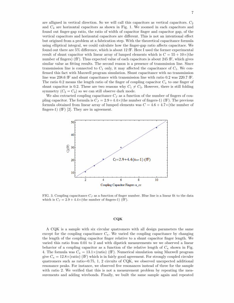
We also extracted coupling capacitance CJ as a function of the number of fingers of cou-pling capacitor. The formula is CJ = 2.9+4.4×(the number of fingers-1) (fF). The previousformula obtained from linear array of lumped elements was C = 4.6 + 4.7×(the number offingers-1) (fF) [2]. They are in agreement.
FIG. 3. Coupling capacitance CJ as a function of finger number. Blue line is a linear fit to the datawhich is CJ = 2.9 + 4.4×(the number of fingers-1) (fF).
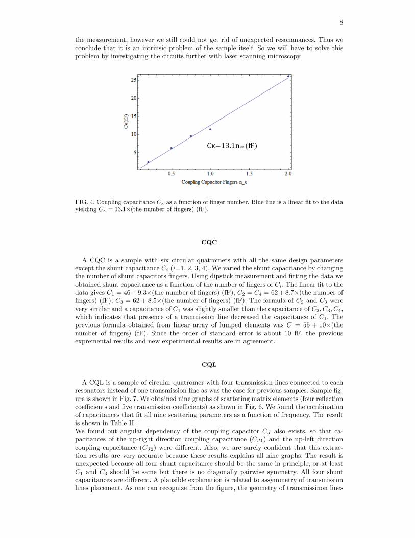
CQK
A CQK is a sample with six circular quatromers with all design parameters the sameexcept for the coupling capacitance Cκ. We varied the coupling capacitance by changingthe length of the coupling capacitor finger relative to a shunt capacitor finger length. Wevaried this ratio from 0.01 to 2 and with dipstick measurements we we observed a linearbehavior of a coupling capacitor as a function of the relative length of Cκ shown in Fig.4. The formula was Cκ = 13.1×(ratio) (fF). Numerical simulation using Maxwell programgive Cκ = 12.8×(ratio) (fF) which is in fairly good agreement. For strongly coupled circulerquatromers such as ratio=0.75, 1, 2 circuits of CQK, we observed unexpected additionalresonance peaks. For instance, we observed five resonances instead of three for the samplewith ratio 2. We verified that this is not a measurement problem by repeating the mea-surements and adding wirebonds. Finally, we built the same sample again and repeated
8
the measurement, however we still could not get rid of unexpected resonanances. Thus weconclude that it is an intrinsic problem of the sample itself. So we will have to solve thisproblem by investigating the circuits further with laser scanning microscopy.
FIG. 4. Coupling capacitance Cκ as a function of finger number. Blue line is a linear fit to the datayielding Cκ = 13.1×(the number of fingers) (fF).
CQC
A CQC is a sample with six circular quatromers with all the same design parametersexcept the shunt capacitance Ci (i=1, 2, 3, 4). We varied the shunt capacitance by changingthe number of shunt capacitors fingers. Using dipstick measurement and fitting the data weobtained shunt capacitance as a function of the number of fingers of Ci. The linear fit to thedata gives C1 = 46 + 9.3×(the number of fingers) (fF), C2 = C4 = 62 + 8.7×(the number offingers) (fF), C3 = 62 + 8.5×(the number of fingers) (fF). The formula of C2 and C3 werevery similar and a capacitance of C1 was slightly smaller than the capacitance of C2, C3, C4,which indicates that presence of a tranmission line decreased the capacitance of C1. Theprevious formula obtained from linear array of lumped elements was C = 55 + 10×(thenumber of fingers) (fF). Since the order of standard error is about 10 fF, the previousexpremental results and new experimental results are in agreement.
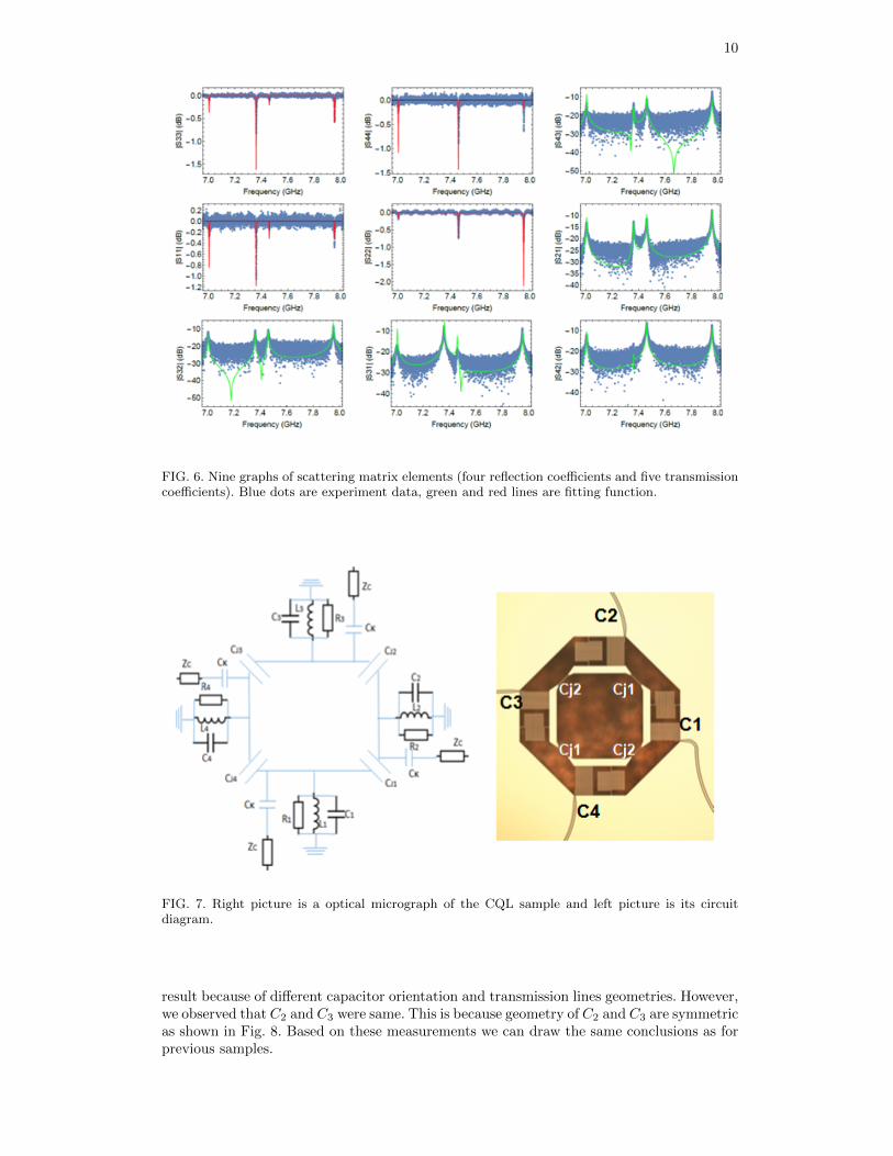
CQL
A CQL is a sample of circular quatromer with four transmission lines connected to eachresonators instead of one transmission line as was the case for previous samples. Sample fig-ure is shown in Fig. 7. We obtained nine graphs of scattering matrix elements (four reflectioncoefficients and five transmission coefficients) as shown in Fig. 6. We found the combinationof capacitances that fit all nine scattering parameters as a function of frequency. The resultis shown in Table II.We found out angular dependency of the coupling capacitor CJ also exists, so that ca-pacitances of the up-right direction coupling capacitance (CJ1) and the up-left directioncoupling capacitance (CJ2) were different. Also, we are surely confident that this extrac-tion results are very accurate because these results explains all nine graphs. The result isunexpected because all four shunt capacitance should be the same in principle, or at leastC1 and C3 should be same but there is no diagonally pairwise symmetry. All four shuntcapacitances are different. A plausible explanation is related to assymmetry of transmissionlines placement. As one can recognize from the figure, the geometry of transmissinon lines
9
FIG. 5. Shunt capacitance Ci (i=1, 2, 3, 4) as a function of finger number. Blue line is a linear fitto the data.
TABLE II. Design parameter extraction result of CQL.
are assymmetric. Hence in order to get a good symmetry, we should design a new samplewith exactly same shape and geometry of all four transmission lines.
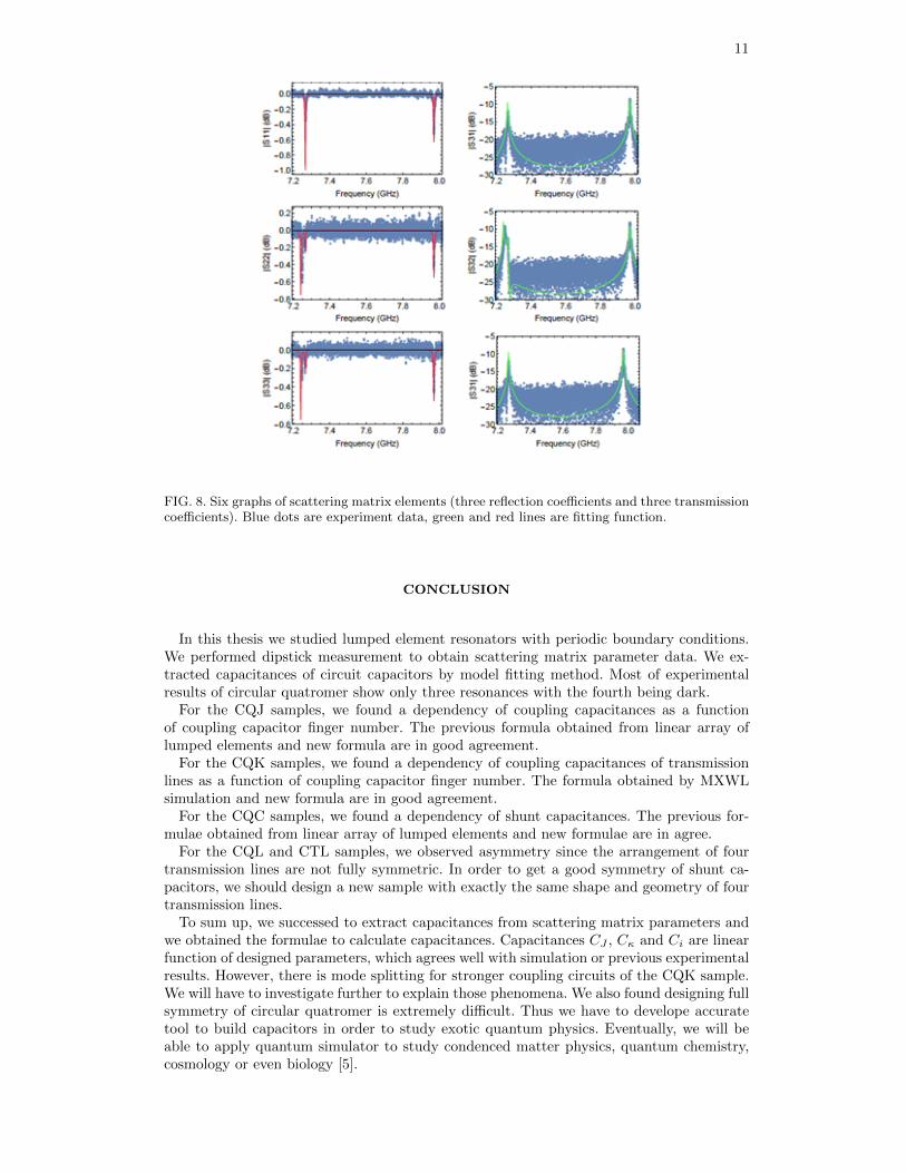
CTL
A CTL is a sample of circular trimer with four transmission lines connected to eachresonators instead of one transmission line. We obtained six graphs of scattering matrixelements (three reflection coefficients and three transmission coefficients) and found thecombination of capacitances that could fit all six graphs. The result is shown in Table III.
TABLE III. Shunt capacitance and coupling capacitor extraction result of CTL.
We observe that all three shunt capacitances are again not the same, which is not a surprising
10
FIG. 6. Nine graphs of scattering matrix elements (four reflection coefficients and five transmissioncoefficients). Blue dots are experiment data, green and red lines are fitting function.
FIG. 7. Right picture is a optical micrograph of the CQL sample and left picture is its circuitdiagram.
result because of different capacitor orientation and transmission lines geometries. However,we observed that C2 and C3 were same. This is because geometry of C2 and C3 are symmetricas shown in Fig. 8. Based on these measurements we can draw the same conclusions as forprevious samples.
11
FIG. 8. Six graphs of scattering matrix elements (three reflection coefficients and three transmissioncoefficients). Blue dots are experiment data, green and red lines are fitting function.
CONCLUSION
In this thesis we studied lumped element resonators with periodic boundary conditions.We performed dipstick measurement to obtain scattering matrix parameter data. We ex-tracted capacitances of circuit capacitors by model fitting method. Most of experimentalresults of circular quatromer show only three resonances with the fourth being dark.
For the CQJ samples, we found a dependency of coupling capacitances as a functionof coupling capacitor finger number. The previous formula obtained from linear array oflumped elements and new formula are in good agreement.
For the CQK samples, we found a dependency of coupling capacitances of transmissionlines as a function of coupling capacitor finger number. The formula obtained by MXWLsimulation and new formula are in good agreement.
For the CQC samples, we found a dependency of shunt capacitances. The previous for-mulae obtained from linear array of lumped elements and new formulae are in agree.
For the CQL and CTL samples, we observed asymmetry since the arrangement of fourtransmission lines are not fully symmetric. In order to get a good symmetry of shunt ca-pacitors, we should design a new sample with exactly the same shape and geometry of fourtransmission lines.
To sum up, we successed to extract capacitances from scattering matrix parameters andwe obtained the formulae to calculate capacitances. Capacitances CJ , Cκ and Ci are linearfunction of designed parameters, which agrees well with simulation or previous experimentalresults. However, there is mode splitting for stronger coupling circuits of the CQK sample.We will have to investigate further to explain those phenomena. We also found designing fullsymmetry of circular quatromer is extremely difficult. Thus we have to develope accuratetool to build capacitors in order to study exotic quantum physics. Eventually, we will beable to apply quantum simulator to study condenced matter physics, quantum chemistry,cosmology or even biology [5].
12
BIBLIOGRAPHY
[1] M. A. Nielsen and I. L. Chuang, Quantum Computation and Quantum Information. Cam-bridge ; New York: Cambridge University Press, 1 ed., 2000.
[2] Antonio Rubio Abadal, Josephson Parametric Amplifiers with Lumped element CoupledResonators. Master Thesis, ETH Zurich, Apr. 2015.
[3] Arno Bargerbos, Coupled Lumped-element Resonators with Periodic Boundary Conditions.Semester Thesis, ETH Zurich, Oct. 2015.
[4] Georgescu, I. M., Ashhab, S., and Nori, F. (2014). Quantum simulation. Reviews of ModernPhysics, 86(1), 153.
[5] Devoret, M. H., and Schoelkopf, R. J. (2013). Superconducting circuits for quantum informa-tion: an outlook. Science, 339(6124), 1169-1174.
[6] Walker, J., Halliday, D., Resnick, R., Resnick, R., and Resnick, R. (2008). Fundamentals ofphysics. New York: Wiley.
[7] Russer, J. A., and Russer, P. (2012, February). Lagrangian and Hamiltonian formulations forclassical and quantum circuits,”. In Proc. 7th Vienna Conference on Mathematical Modelling,MATHMOD, Vienna.
[8] C. Cohen-Tannoudji, J. Dupont-Roc, and G. Grynberg, Photons and Atoms: Introduction toQuantum Electrodynamics. Physics textbook, Weinheim: Wiley, nachdr. ed., 2004.
[9] D. J. Griffiths, Introduction to Quantum Mechanics. Upper Saddle River, NJ: Pearson PrenticeHall, 2nd ed ed., 2005.
[10] Pozar, D. M. (2009). Microwave engineering. John Wiley and Sons.