CHARACTERIZING SENSITIVE CMOS RADIATION DETECTOR Hank Javan, University of Memphis, T N Key words: CMOS, Semiconductor, Radiation, Detector ABSTRACT Semiconductor sensors cover a wide range of electromagnetic spectrum for detecting nuclear-particle radiation. The most important properties of these detectors are their sensitivity Le. their ability to low level radiation, charge transport, efficiency (electron-hole pair creation), and their response time. This article addresses the sensitivity of these devices. Following methods can increase the sensitivity of any electronic sensors: 1 . Proper selection of the material with respect to the desired radiation detection, i.e matching the energy gap of the device, E , , to the energy of incoming radiation. 2. Application of proper process technology, such as CMOS, BiCMOS, etc. 3 . Fabrication technology Le. using proper doping, substrate, etc. 4. Finally design of external circuitry. This paper reports the investigation of the circuitry of a newly developed CMOS a particle radiation detector and characterization of its sensitivity. Also discusses the effect of external derivation of analytical expression for the sensitivity and compares the theoretical prediction with the experimental values. In addition, the effect of radiation on the threshold voltage is discussed as well as an increase in sensitivity due to radiation. Finally, a method is suggested to obtain a n optimum performance. I. INTRODUCTION Semiconductor detectors such as photoconductor, photodiode, and phototransistor operate on the principle of electron-hole pair generation and charge transport mechanism. A good semiconductor sensor device should have high detector efficiency, large collecting area, low leakage current, and be economically feasible[l]. A cross section o f a silicon-on-insulator (SOI) photodiode and one DepMOS-DepFET for X-ray detection are shown a s a reference in figure la and l b in order to assist the reader to understand the current technology used in this field [2]. I 4 ..SI @) Fig. 1- (a) A cross section of photo diode @) Cross section of a nuclear radiation detector 0-7803-7252-2/02/$10.00Q ZOO2 IEEE Proceedings IEEE SoutheastCon 2002 28 Authorized licensed use limited to: VELLORE INSTITUTE OF TECHNOLOGY. Downloaded on January 27, 2009 at 11:25 from IEEE Xplore. Restrictions apply.
Semiconductor sensors cover a widerange of electromagnetic spectrum fo r detectingnuclear-particle radiation. The most impo rtantprope rties of these detectors ar e their sensitivityLe. their ability to low level radiation, chargetransport, efficiency (electron-hole paircreation), an d the ir response time. This articleaddresses the sensitivity of these devices.
Following m ethods can increase th e sensitivity ofany electronic sensors:
1. Proper selection of the material withrespect to the desired radiationdetection, i.e ma tching the energy ga pof the device, E,, to the energy ofincoming radiation.
2. Application of proper processtechnology, such as CMOS, BiCMOS,etc.
3. Fabrication technology Le. usingpr op er doping, substra te, etc.
4. Finally design of extern al circuitry.
This pa per rep orts the investigation of the
circuitry of a newly developed CMOS a particleradiation detector and characterization of itssensitivity. Also discusses the effect of external
power supply connection on the sensitivity,derivation of analytical expression for thesensitivity and compares the theoreticalprediction with the experimen tal values. In
addition, the effect of radiation on the thresholdvoltage is discussed as well as an increase insensitivity due to radiation. Finally, a method is
suggested to obtain a n optimum performance.
I. INTRODUCTION
Semiconductor detectors such as
photoconductor, photodiode, and phototransistor
operate on the principle of electron-hole pairgeneration and charge transport mechanism. Agood semiconductor sensor device should have high
detector efficiency, large collecting area, lowleakage current, and be economically feasible[l]. A
cross section of a silicon-on-insulator (SOI)photodiode and one DepMOS-DepFET for X-raydetection are shown as a reference in figure l a andl b in order to a ssist the reader to understand the
Among the different technologies, MOS and reduction of thre shold voltage due to radiation isCMO S method offer an excellent choice for nuclear examined.particle detection. This is due to their small leakagecurrent, high input impedance and excellent lownoise figure. In addition, these circuits have a realestate advantage for IC techno logy. Figure 2 showsthe circuit of a new ly developed CMOS D type flip-
flop radiation de tector for a particle.
Q
BR2ES
P
ID0
ENABLE a
Fig. 2- Circuitry of aD-we flip-flopused for nuclear radiation detec tion using CMOS
The heart of this circuit is the incorporationof D type flip-flop used as a single event radiation
detector. Flip-flops are made of logic gates simplyby use of feedback circuits. The NAND gates aretransistor inverters. One such a flip-flop, called R-S
flip-flop is shown in figure 3(a) with itsimplementation to obtain a D type flip-flop in figure
3@).
D type flip-flop can be used for single eventcounter (SEC ) either by direct radiation through thewindows or via the input circuitry as shown in
figure. The problem with such a circuit is the needfor high sensitivity under low radiation condition.
Circuit shown in figure 2 is the implementation ofsuch a flip-flop in cascade-cascode mode to obtainthe single event count by shifting the data from theinput to the output. In the following the operationof this circuit is discussed first, then the possibilityof increasing its sensitivity by m odifying the powersupply connection is investigated . Finally the
Fig.3- (a) AR-S flip-flop using nor @es@) Implementation of D-flip-flop using R-S ff
11-CIRCUITDESCRIPTION
Referring to figure 2, radiation is detected
by D-type flip-flop at its input. This flip-flop ismade of CMOS technology to increase itssensitivity and to reduce noise, as discussed in theprevious section. This flip-flop will be activatedupon irradiation and assertion of the Enable line.Charge is transferred to the next CMOS by theinter-coupling capacitor to the last stage.
The original circuit uses one power supplyV d d as shown. However it is shown experimentallythat isolating V d d and using a separate supply forthe last stage has increased the sensitivity of thisdetector as shown and will be discussed below. Wenow develop an analytical expression to show thatthis method of power supply connection can in factincrease the sensitivity of this detector. In addition,
Proceedings IEEE Southeastcon 2002
29
Authorized licensed use limited to: VELLORE INSTITUTE OF TECHNOLOGY. Downloaded on January 27, 2009 at 11:25 from IEEE Xplore. Restrictions apply.
by providing another expression for the thresholdvoltage, V, will be shown that this configuration
also reduces the threshold voltage, thus furtherincreasing sensitivity.
111-EFFECT OF OFFSET VOLTAGE
The drain current of an EnhancementMO SFET is given by [4];
The plot ( I / At) of this equation for the parametervalues assumed are shown in Figure 4, and are
In this equation k is a function of the geometry of
the channel, its value is about 0.3mAlv2, v d is the
drain supply voltage, and V, is the thresholdvoltage, the minimum voltage required to turn on
the FET. The value of VI depends on the dielectricmaterial used for the gate insulation. Its value
typically ranges fiom 1 to 3 volt [5]. However,research is under way to decrease this value to0.5V. Referring to Figure 2, the last transistor isisolated from the power supply Vdd and i sconnected to V,,T. It is important to note that this
voltage, V,,T is not the usual offset voltage we useto balance the transistor output to zero in theabsence of input. This voltage is primarily used toincrease the sensitivity as will be shown below.The gate of this MOS is connected to the intemalcapacitor of the previous stage; thus V, in the aboveequation can be expressed as;
In this equation C is the capacitance value of the
intracapacitor, Q is the charge due to radiation, I is
the resulting current, and At is the event time. We
have used At instead of dt to indicate that this is adiscrete event. Returning to the last MOS which isconnected to V,,T, since this transistor is on, itscurrent 4can be written as
%. is the on resistance of the transistor. Use of %.is justified since the charge transfer or the radiationeffect is considered to be single event, and thus the
transistor is operated as a switch, being either ONor OFF. Inserting equation (3 ) and (2) in ( 1 ) weobtain for the Upset Rate;
V , = V , = Q / C = L A t l C (2)
Id = Vod %n (3)
l / A t = ( ~ / . I ( v , n / k % " ) + V t ) C (4)
ProceedingsIEEE Southeastcon ZOO2
30
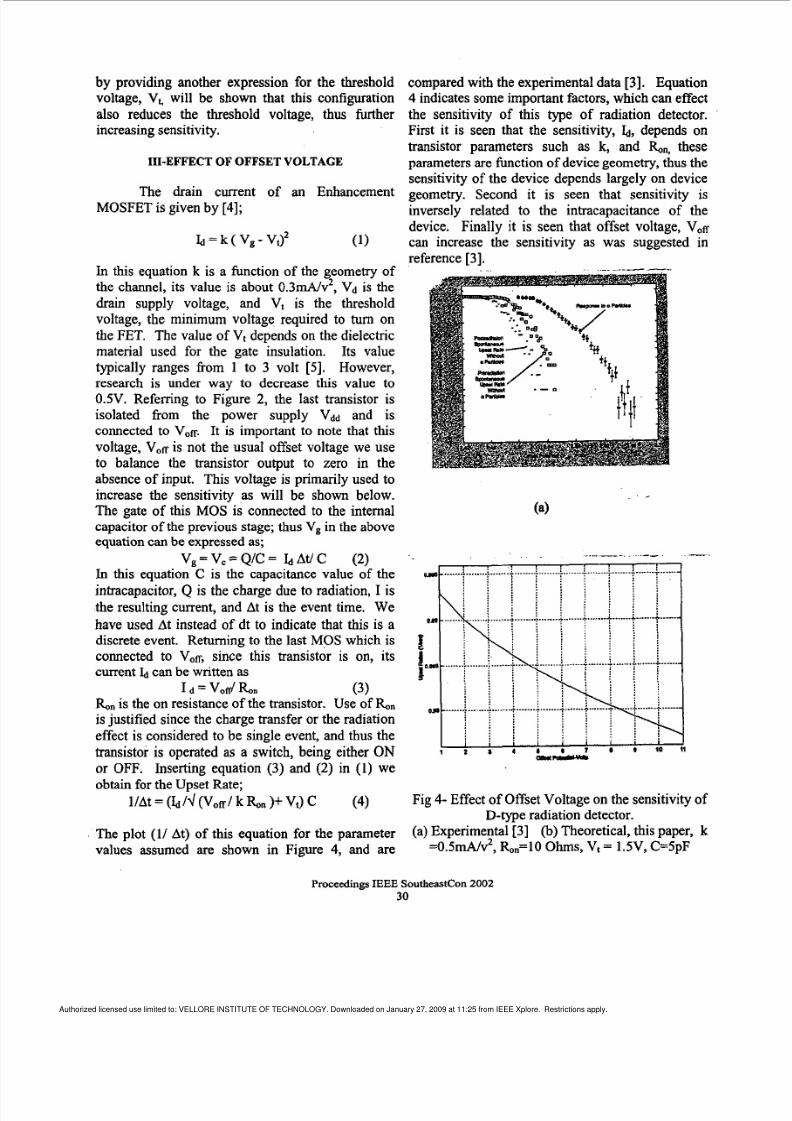
compared with the experimental data [3]. Equation4 indicates some important factors, which can effectthe sensitivity of this type of radiation detector.First it is seen that the sensitivity, 4,depends on
transistor parameters such as k, an d &% theseparameters are function of device geometry, thus thesensitivity of the device depends largely on devicegeometry. Second it is seen that sensitivity isinversely related to the intracapacitance of thedevice. Finally it is seen that offset voltage, V,,Tcan increase the sensitivity as was suggested inreference [3].
.. ..
Fig 4- Effect of Offset Vo ltage on the sensitivity ofD-type radiation detector.
(a) Experimental [3] (b)Theore tical, this paper, k
=O.SmA /? , &"=lo Ohms, V, = lS V , C=SpF
Authorized licensed use limited to: VELLORE INSTITUTE OF TECHNOLOGY. Downloaded on January 27, 2009 at 11:25 from IEEE Xplore. Restrictions apply.
Hank java n received his B.S.E.E., M.S.E.E., and Ph.D. in1965, 1970, and 1980 respectively. Since his graduation hehas worked for several companies, has taught in severaluniversities, and has held fellowships with NASA and N A V Y .Dr. Javan is principle author of over twenty referee articlespublished in intemational journals. He is a senior member ofIEEE and holds Professional Engineering License from Stateof Tennessee. Currently he is an Assistant Professor withUniversity of Memphis.
1.
2.
Can increase the sensitivity of D-typeradiation detector mentioned in thispaper.Can reduce the threshold voltage, thuscausing further incre ase in sensitivity.
In addition our express ion for sensitivity equation 6
suggest that transistor parameter such as k, and bncan play an important rule in determining thesensitivity of CM OS radiation detector device. Wehave also established an optimum value for theoffset voltage as given by equation (7).
REFERENCES
[l]. J.Fraden, “AIP Hankbook of Modem Sensors“,Am erican Institute of Physics , 1993, pp 471-481.