RTO
RTCVDpoly
RTCVDnitride
CleanModule
Loadlock
ellipso-meter
foup
NTU GIEE NanoSiOE 2005/06/18 1
CMOS/SiGe BiCMOS 2.4GHz RF Linear PCMOS/SiGe BiCMOS 2.4GHz RF Linear P
ower Amplifier on PCB Moduleower Amplifier on PCB Module
指導教授:劉致為 博士學生:賴宏諱
台灣大學電子工程學研究所
RTO
RTCVDpoly
RTCVDnitride
CleanModule
Loadlock
ellipso-meter
foup
NTU GIEE NanoSiOE 2005/06/18 2
OutlineOutline
IntroductionIntroduction
Basic Concepts and Design FlowBasic Concepts and Design Flow
CMOS Power AmplifierCMOS Power Amplifier
SiGe BiCMOS Power Amplifier SiGe BiCMOS Power Amplifier
PCB Module Fabrication PCB Module Fabrication
SummarySummary
RTO
RTCVDpoly
RTCVDnitride
CleanModule
Loadlock
ellipso-meter
foup
NTU GIEE NanoSiOE 2005/06/18 3
OutlineOutline
IntroductionIntroduction
Basic Concepts and Design FlowBasic Concepts and Design Flow
CMOS Power AmplifierCMOS Power Amplifier
SiGe BiCMOS Power Amplifier SiGe BiCMOS Power Amplifier
PA Module AssemblyPA Module Assembly
SummarySummary
RTO
RTCVDpoly
RTCVDnitride
CleanModule
Loadlock
ellipso-meter
foup
NTU GIEE NanoSiOE 2005/06/18 4
Wireless TechnologyWireless TechnologyTechnology Standard Usage Data Rate Range Frequency
UWB 802.15.3a WPAN 1.3Gbps 30 feet 3.1-10.6Ghz
Wi-Fi 802.11b WLAN 11Mbps 100 feet 2.4Ghz
Wi-Fi 802.11a/g WLAN 54Mbps 100 feet 5.8/2.4Ghz
Wi-Fi 802.11n WLAN >100Mbps 100 feet 5.8/2.4Ghz
WiMax 802.16a WMAN 75Mbps 4-6 miles 2-11Ghz
WiMax 802.16e Mobile, WMAN 30Mbps 1-3 miles 2-6Ghz
WCDMA 3G Mobile 2Mbps 1-5 miles 1.8~2.1Ghz
RTO
RTCVDpoly
RTCVDnitride
CleanModule
Loadlock
ellipso-meter
foup
NTU GIEE NanoSiOE 2005/06/18 5
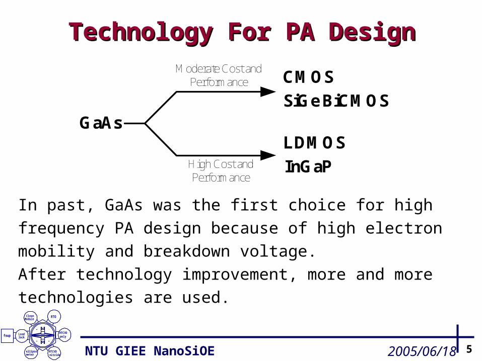
Technology For PA DesignTechnology For PA Design
GaAs
CMOS
SiGe BiCMOS
LDMOS
InGaP
Moderate Cost and Performance
High Cost and Performance
In past, GaAs was the first choice for high frequency PA desi
gn because of high electron mobility and breakdown voltage.
After technology improvement, more and more technologies
are used.
RTO
RTCVDpoly
RTCVDnitride
CleanModule
Loadlock
ellipso-meter
foup
NTU GIEE NanoSiOE 2005/06/18 6
Why CMOS and SiGe BiCMOS?Why CMOS and SiGe BiCMOS?
VCO
LNA
Mixer
Mixer
PA LPF
BPF Baseband
Baseband
Antenna
Fabricated by CMOS
Fabricated by other technology
RTO
RTCVDpoly
RTCVDnitride
CleanModule
Loadlock
ellipso-meter
foup
NTU GIEE NanoSiOE 2005/06/18 7
VCO
LNA
Mixer
Mixer
PA LPF
BPF Baseband
Baseband
Antenna
Fabricated by Si-based
Why CMOS and SiGe BiCMOS?Why CMOS and SiGe BiCMOS?
RTO
RTCVDpoly
RTCVDnitride
CleanModule
Loadlock
ellipso-meter
foup
NTU GIEE NanoSiOE 2005/06/18 8
OutlineOutlineIntroductionIntroduction
Basic Concepts and Design FlowBasic Concepts and Design Flow
CMOS Power AmplifierCMOS Power Amplifier
SiGe BiCMOS Power Amplifier SiGe BiCMOS Power Amplifier
PA Module AssemblyPA Module Assembly
SummarySummary
RTO
RTCVDpoly
RTCVDnitride
CleanModule
Loadlock
ellipso-meter
foup
NTU GIEE NanoSiOE 2005/06/18 9
Classification of Power Classification of Power AmplifierAmplifier
Linear: for non-constant envelope modulation (ex: OFDM)
Class A : 100% duty cycle, effmax= 50%
Class B : 50% duty cycle, effmax= 78.5%
Class C : <50% duty cycle, effmax=78.5%~100%
Class AB: 50%~100% duty cycle, effmax=50%~78.5%
Nonlinear: for constant envelope modulation (ex: GMSK)
Class D: ideal 100% efficiency
Class E: ideal 100% efficiency
Class F: ideal 100% efficiency
RTO
RTCVDpoly
RTCVDnitride
CleanModule
Loadlock
ellipso-meter
foup
NTU GIEE NanoSiOE 2005/06/1815
Linear Power AmplifierLinear Power Amplifier
VGS
Vds
ZLoad
Ids
VDD
ids
V0
Vq
VtGate voltage
VIN
Idc
ImaxiD
0
Drain current
0
VDSV0
2ππ 3π 4π
Drain voltage
ω t
VDD
Vds=VDD+ids*ZLoad
RTO
RTCVDpoly
RTCVDnitride
CleanModule
Loadlock
ellipso-meter
foup
NTU GIEE NanoSiOE 2005/06/1816
Load LineLoad Line
Ropt
=(Vbreakdown
-Vknee
)/Ids
VGS
operation point
Vbreakdown
Vknee
I DS
VDS
Vin and iD swing
Vo swing
RTO
RTCVDpoly
RTCVDnitride
CleanModule
Loadlock
ellipso-meter
foup
NTU GIEE NanoSiOE 2005/06/1817
Pure Resistance ZPure Resistance ZLoadLoad
RTO
RTCVDpoly
RTCVDnitride
CleanModule
Loadlock
ellipso-meter
foup
NTU GIEE NanoSiOE 2005/06/1818
∠∠ZZLoadLoad from 0 from 0o o to 90to 90oo
RTO
RTCVDpoly
RTCVDnitride
CleanModule
Loadlock
ellipso-meter
foup
NTU GIEE NanoSiOE 2005/06/1819
∠∠ZZLoadLoad from 0 from 0o o to 90to 90oo
Vds=Idsx50∠30o →Vds leads more 30o to Ids
RTO
RTCVDpoly
RTCVDnitride
CleanModule
Loadlock
ellipso-meter
foup
NTU GIEE NanoSiOE 2005/06/1820
Load Line for different PLoad Line for different P inin
RTO
RTCVDpoly
RTCVDnitride
CleanModule
Loadlock
ellipso-meter
foup
NTU GIEE NanoSiOE 2005/06/1821
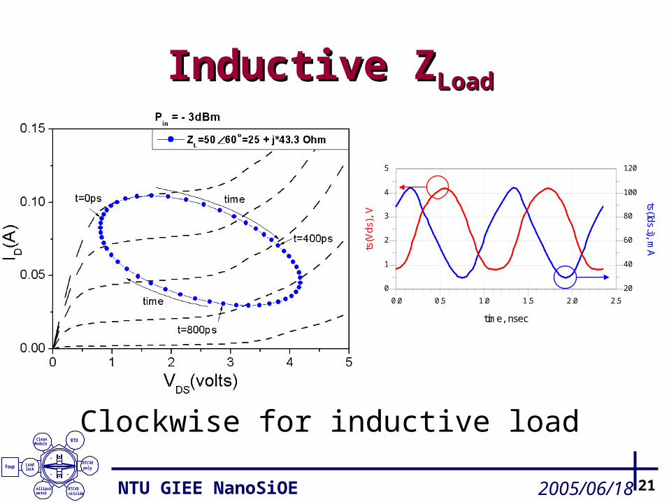
Inductive ZInductive ZLoadLoad
0.5 1.0 1.5 2.00.0 2.5
1
2
3
4
0
5
40
60
80
100
20
120
time, nsec
ts(Ids.i), mAts
(Vds
), V
Clockwise for inductive load
RTO
RTCVDpoly
RTCVDnitride
CleanModule
Loadlock
ellipso-meter
foup
NTU GIEE NanoSiOE 2005/06/1822
Capacitive ZCapacitive ZLoadLoad
0.5 1.0 1.5 2.00.0 2.5
1.5
2.0
2.5
3.0
3.5
1.0
4.0
40
50
60
70
80
90
30
100
time, nsec
ts(Ids.i), mAts
(Vds
), V
Counterclockwise for capacitive load
RTO
RTCVDpoly
RTCVDnitride
CleanModule
Loadlock
ellipso-meter
foup
NTU GIEE NanoSiOE 2005/06/1825
Design FlowDesign FlowEstablish Specification According to
Standard & Product Data Sheet
Circuit Topology DeterminationUnit Cell Selection & Characterization
Circuit Topology Determination & Output Power Planning
Design Each Stage: DC, Small & Large Signal Simulation
Layout, Parasitic Extraction and Post-layout Simulation
Adding Matching and Bias circuit
PCB Design (Loadpull, TRL & Matching)
Performance Measurement
RTO
RTCVDpoly
RTCVDnitride
CleanModule
Loadlock
ellipso-meter
foup
NTU GIEE NanoSiOE 2005/06/1826
OutlineOutlineIntroductionIntroduction
Basic Concepts and Design FlowBasic Concepts and Design Flow
CMOS Power AmplifierCMOS Power Amplifier
SiGe BiCMOS Power Amplifier SiGe BiCMOS Power Amplifier
PA Module AssemblyPA Module Assembly
SummarySummary
RTO
RTCVDpoly
RTCVDnitride
CleanModule
Loadlock
ellipso-meter
foup
NTU GIEE NanoSiOE 2005/06/1827
Self-Biased Cascode Self-Biased Cascode
VoutVin
Vdc
1 2 3 4 50 6
20
40
60
80
0
100
VDS
casc
ode.
i, m
AC
S.i,
mA
Vout
Vin
Vdc
R
C
RTO
RTCVDpoly
RTCVDnitride
CleanModule
Loadlock
ellipso-meter
foup
NTU GIEE NanoSiOE 2005/06/1828
Schematic of 0.25um CMOS PASchematic of 0.25um CMOS PA
Unit Device : 64 fingers 10/0.25um RF NMOSVDD=3.3V
X1
X2 X6
X4
RTO
RTCVDpoly
RTCVDnitride
CleanModule
Loadlock
ellipso-meter
foup
NTU GIEE NanoSiOE 2005/06/1829
Bond wire and Pad ModelBond wire and Pad Model
80 µm
80 µm0.082 pF
625 ohmM5
1mm
1nHQ=72.6@2GHz
RTO
RTCVDpoly
RTCVDnitride
CleanModule
Loadlock
ellipso-meter
foup
NTU GIEE NanoSiOE 2005/06/1830
Circuit LayoutCircuit Layout
Chip size : 0.98mm x 0.73mm=0.7154mm2
RTO
RTCVDpoly
RTCVDnitride
CleanModule
Loadlock
ellipso-meter
foup
NTU GIEE NanoSiOE 2005/06/1831
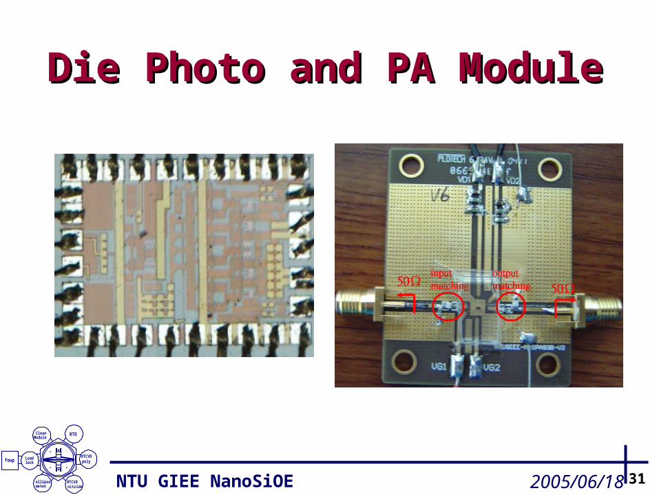
Die Photo and PA ModuleDie Photo and PA Module
RTO
RTCVDpoly
RTCVDnitride
CleanModule
Loadlock
ellipso-meter
foup
NTU GIEE NanoSiOE 2005/06/1832
MeasurementMeasurement
Linear gain=26dB, P1dB=18.5dBm, Psat=21.8dBm
Select VGS=1.1V, VDD=3.3V
Current versus Pin for different VGS
Output power and gain versus Pin
RTO
RTCVDpoly
RTCVDnitride
CleanModule
Loadlock
ellipso-meter
foup
NTU GIEE NanoSiOE 2005/06/1833
MeasurementMeasurement
IDC=170mA, PAE@P1dB=13%, maximum PAE=23%
2.2 2.4 2.6 2.82.0 3.0
-40
-30
-20
-10
-50
0
freq, GHz
dB(S
(1,1
))dB
(S(1
,2))
dB(S
(2,2
))
At 2.45GHz, S11=-12.3dB, S22=-16.4dB, S12=-40.7dB
IDC and PAE versus Pin S-parameters
RTO
RTCVDpoly
RTCVDnitride
CleanModule
Loadlock
ellipso-meter
foup
NTU GIEE NanoSiOE 2005/06/1834
SummarySummaryFrequency (GHz) 2.4~2.484
VDD (Volts) 3.3
Psat (dBm) 21.8
P1dB(dBm) 18.5
Linear Gain (dB) 26
IDC (mA) 170
IDC (mA)@P1dB 177
S11(dB) -12.3
S12(dB) -40.7
S22(dB) -16.4
PAE@P1dB(%) 13
RTO
RTCVDpoly
RTCVDnitride
CleanModule
Loadlock
ellipso-meter
foup
NTU GIEE NanoSiOE 2005/06/1835
Schematic of 0.18um CMOS PASchematic of 0.18um CMOS PA
Unit Device : 64 fingers 2.5/0.18um RF NMOSVDD=2.5V
X1
X2 X6
X4
RTO
RTCVDpoly
RTCVDnitride
CleanModule
Loadlock
ellipso-meter
foup
NTU GIEE NanoSiOE 2005/06/1836
Bias Control CircuitBias Control Circuit
Powerdetector
VD1
VDD
C2C1
R3
R1
R2VGS2
Sensing power
RTO
RTCVDpoly
RTCVDnitride
CleanModule
Loadlock
ellipso-meter
foup
NTU GIEE NanoSiOE 2005/06/1837
SimulationSimulation
1 dB compressed point→ +1.3dBm
RTO
RTCVDpoly
RTCVDnitride
CleanModule
Loadlock
ellipso-meter
foup
NTU GIEE NanoSiOE 2005/06/1838
OutlineOutlineIntroductionIntroduction
Basic Concepts and Design FlowBasic Concepts and Design Flow
CMOS Power AmplifierCMOS Power Amplifier
SiGe BiCMOS Power AmplifierSiGe BiCMOS Power Amplifier
PA Module AssemblyPA Module Assembly
SummarySummary
RTO
RTCVDpoly
RTCVDnitride
CleanModule
Loadlock
ellipso-meter
foup
NTU GIEE NanoSiOE 2005/06/1839
Schematic of 0.35um SiGe PASchematic of 0.35um SiGe PA
Input
OUTPUT
stage2bias
circuit
λ /4 λ /4 λ /4
Vcc VccVcc
Q1 Q2 Q3
stage1bias
circuit
stage3bias
circuit
Unit Device : hw153c2 (emitter:20.3um/0.9um)
Vcc=3.3V, Q1:4X, Q2:16X, Q3:48X
RTO
RTCVDpoly
RTCVDnitride
CleanModule
Loadlock
ellipso-meter
foup
NTU GIEE NanoSiOE 2005/06/1840
Bond-wire and Pad ModelBond-wire and Pad Model
80 µm
80 µm 40 µm0.23 pF
180 ohm
M1, M2 & M3
1mm
1nHQ=72.6@2GHz
RTO
RTCVDpoly
RTCVDnitride
CleanModule
Loadlock
ellipso-meter
foup
NTU GIEE NanoSiOE 2005/06/1841
Active Bias CircuitActive Bias Circuit
Vcc
R2R1
R3R4
C1
Q1
Q2
VBE
Main signal path
DC base current
IE1
+
-VBE1
VBE1
IE1
-40 -30 -20 -10 0 10 209
101112131415161718
hw153c2x2 + 0.375 nH LE
Gai
n (
dB
)
Pout
(dBm)
VBE
=0.81V V
BE=0.84V
VBE
=0.87V
Linearity improvement
RTO
RTCVDpoly
RTCVDnitride
CleanModule
Loadlock
ellipso-meter
foup
NTU GIEE NanoSiOE 2005/06/1842
Active Bias CircuitActive Bias Circuit
Vcc
R2R1
R3R4
C1
Q1
Q2
VBE
Main signal path
DC base current
IE1
+
-VBE1
Temperature Compensation
RTO
RTCVDpoly
RTCVDnitride
CleanModule
Loadlock
ellipso-meter
foup
NTU GIEE NanoSiOE 2005/06/1843
Circuit LayoutCircuit Layout
Die size : 1.36mm x 0.68mm (0.9248mm2 )
RTO
RTCVDpoly
RTCVDnitride
CleanModule
Loadlock
ellipso-meter
foup
NTU GIEE NanoSiOE 2005/06/1844
Die Photo and PA ModuleDie Photo and PA Module
RTO
RTCVDpoly
RTCVDnitride
CleanModule
Loadlock
ellipso-meter
foup
NTU GIEE NanoSiOE 2005/06/1845
MeasurementMeasurement
Pout and gain versus Pin PAE and ICC versus Pin
IDC=360mA, PAE@P1dB=15%,
maximum PAE=24%
Linear gain=27.6dB, P1dB=20.7dBm, Psat=25.4dBm
RTO
RTCVDpoly
RTCVDnitride
CleanModule
Loadlock
ellipso-meter
foup
NTU GIEE NanoSiOE 2005/06/1846
MeasurementMeasurement
Data rate=54Mbps, 64QAM OFDM
S-parameters
At 2.45GHz, S11=-12.6dB, S22=-14dB, S12=-39.7dB
Error Vector Magnitude
RTO
RTCVDpoly
RTCVDnitride
CleanModule
Loadlock
ellipso-meter
foup
NTU GIEE NanoSiOE 2005/06/1847
Spectrum MaskSpectrum Mask
Transmit Emission Mask
Frequency/MHz2400 2410 2420 2430 2440 2450 2460 2470 2480 2490 2500
-87
-77
-67
-57
-47
-37
-27
-17
-7
3
13Transmit Emission Mask
Frequency/MHz2400 2410 2420 2430 2440 2450 2460 2470 2480 2490 2500
-93
-83
-73
-63
-53
-43
-33
-23
-13
-3
7
Pout=17.8dBm (CCK) Pout=15.2dBm (OFDM)
fc=2.45GHz,802.11b,11MB/s,CCK 802.11g,54MB/s, 64QAM OFDM
RTO
RTCVDpoly
RTCVDnitride
CleanModule
Loadlock
ellipso-meter
foup
NTU GIEE NanoSiOE 2005/06/1848
SummarySummaryFrequency (GHz) 2.4~2.484
Vcc (Volts) 3.3
Psat (dBm) 25.4
P1dB(dBm) 20.7
Pout@11b 17.8
Pout@11g 15.2
Linear Gain (dB) 27.6
IDC (mA) 361
IDC (mA)@P1dB 385
S11(dB) -12.6
S12(dB) -39.7
S22(dB) -14
PAE@P1dB(%) 15
RTO
RTCVDpoly
RTCVDnitride
CleanModule
Loadlock
ellipso-meter
foup
NTU GIEE NanoSiOE 2005/06/1849
Loop of Power Control Loop of Power Control
PAVGA
Power Detector
Controller
Antenna
Output signalInput signal
Power detector senses present output power level
and inform the controller by a corresponding DC voltage
RTO
RTCVDpoly
RTCVDnitride
CleanModule
Loadlock
ellipso-meter
foup
NTU GIEE NanoSiOE 2005/06/1850
Power Detector Circuit Power Detector Circuit (( II ))
Vdetect
Diode
Main power flow
Antenna
Vdc
Diode
PA output terminal
Sensing power
Temperature compensation
circuit
Use BC junction for smaller capacitance.
Added a diode to cancel DC offset caused by temperature variation.
RTO
RTCVDpoly
RTCVDnitride
CleanModule
Loadlock
ellipso-meter
foup
NTU GIEE NanoSiOE 2005/06/1851
Power Detector Circuit Power Detector Circuit (( IIII ))VdcVdc
Vdetect+ -
Sensing power
Vi
Ic
Q1 Q2
-10 0 10 20 300.0
0.5
1.0
1.5
2.0
2.5
Vde
tect(v
olts
)Pout(dBm)
25oC
55oC
85oC
Vi=VQ+Vaccosθ
Ic=Isexp(VQ/VT)exp(Vaccosθ/VT) A DC component can be extracted from the term exp(Vaccosθ/VT)
RTO
RTCVDpoly
RTCVDnitride
CleanModule
Loadlock
ellipso-meter
foup
NTU GIEE NanoSiOE 2005/06/1852
Dual Power Amplifier for IEEE Dual Power Amplifier for IEEE 802.11n802.11n
TGn Sync(Task Group n)
Agere, Atheros, Cisco, Intel, InterDigital, Marvell, Mitsubishi , Nortel, Panasonic, Philips, Qualcomm , Samsu
ng, SANYO, Sony, and Toshiba
WWiSE(World Wide Spectrum E
fficiency)
Airgo, Broadcom, Buffalo, Conexant, ETRI, Hughes, Motorola, Nokia, Ralink, Realtek, STMicro, TI, TrellisW
are, and Winbond
The main techniques multiply the data rate :
(1) Spatial multiplexing (MIMO): 2 to 4 Tx/Rx.
(2) Increasing the channel bandwidth: 2040 MHz/channel.
(3) Increasing the constellation size: 64-QAM or Higher
(4) Increasing the coding rate: (3/45/6 or 7/8)
(5) Reducing the guard interval: (800ns400ns)
RTO
RTCVDpoly
RTCVDnitride
CleanModule
Loadlock
ellipso-meter
foup
NTU GIEE NanoSiOE 2005/06/1853
Dual Power Amplifier for IEEE Dual Power Amplifier for IEEE 802.11n802.11n
Die size : 1.98mm x 1.28mm (2.5344mm2 )
RTO
RTCVDpoly
RTCVDnitride
CleanModule
Loadlock
ellipso-meter
foup
NTU GIEE NanoSiOE 2005/06/1854
OutlineOutlineIntroductionIntroduction
Basic Concepts and Design FlowBasic Concepts and Design Flow
CMOS Power AmplifierCMOS Power Amplifier
SiGe BiCMOS Power Amplifier SiGe BiCMOS Power Amplifier
PA Module AssemblyPA Module Assembly
SummarySummary
RTO
RTCVDpoly
RTCVDnitride
CleanModule
Loadlock
ellipso-meter
foup
NTU GIEE NanoSiOE 2005/06/1855
Load Pull SystemLoad Pull System
Signal Generator
PA(Psat: 40dBm)
Power Meter
Power Supply
Spectrum Analyzer
Power Spliter-16dB
IsolatorBias Tee
Source Tuner
DUTLoad Tuner Bias Tee
Power Spliter
Antenuator
First, one tuner remains unchanged, and the other tuner varies to find
the optimal impedance of maximum output power.
Then the latter tuner keeps the optimal impedance, and the former
tuner starts tuning.
After iterated tuning, the optimal ZS and ZL are found.
RTO
RTCVDpoly
RTCVDnitride
CleanModule
Loadlock
ellipso-meter
foup
NTU GIEE NanoSiOE 2005/06/1856
Load Pull& TRL PCBLoad Pull& TRL PCB
344mil344mil
648mil
648mil
344mil 344mil
Load Pull PCB TRL PCB(Through, Reflect, Load)
Use TRL to eliminate effect of 344mil TL line.
FR4 648mil/28mil TL line equals toλ/4 of 2.45GHz
Die
Use load pull PCB to find optimal ZS and ZL for maximum power output
RTO
RTCVDpoly
RTCVDnitride
CleanModule
Loadlock
ellipso-meter
foup
NTU GIEE NanoSiOE 2005/06/1857
Matching PCBMatching PCB
Matching PCB
Photo of matched PA Module
Passive Device: Murata SMD
RTO
RTCVDpoly
RTCVDnitride
CleanModule
Loadlock
ellipso-meter
foup
NTU GIEE NanoSiOE 2005/06/1858
Power ContourPower Contour
After doing load pull on matched PA module, the optimal ZL is near 50 Ohm.It means that the matching is well done.
RTO
RTCVDpoly
RTCVDnitride
CleanModule
Loadlock
ellipso-meter
foup
NTU GIEE NanoSiOE 2005/06/1859
OutlineOutlineIntroductionIntroduction
Basic Concepts and Design FlowBasic Concepts and Design Flow
CMOS Power AmplifierCMOS Power Amplifier
SiGe BiCMOS Power Amplifier SiGe BiCMOS Power Amplifier
PA Module AssemblyPA Module Assembly
SummarySummary
RTO
RTCVDpoly
RTCVDnitride
CleanModule
Loadlock
ellipso-meter
foup
NTU GIEE NanoSiOE 2005/06/1860
SummarySummary A 2.4GHz 0.25um CMOS PA achieves linear gain=26dB, Psat=21.8dBm,
P1dB=18.5dBm and maximum PAE=23%.
We designed a 2.4GHz 0.18um CMOS PA with bias control circuit. From simulation, the 1dB compressed point increases 1.3dBm.
A 2.4GHz 0.35um SiGe BiCMOS PA achieves linear gain=27.6dB, Psat=
20.4dBm, P1dB=20.7dBm and maximum PAE=24%. Under IEEE 802.11
b operation, maximum Pout=17.8dBm; under IEEE 802.11g operation, maximum Pout=15.2dBm.
Two types power detector are designed.
Based on SiGe PA topology, we design a dual power amplifier for new standard 802.11n.


![HORIZONTAL CURRENT BIPOLAR TRANSISTOR (HCBT) A …performance Si/SiGe BiCMOS technologies [4] prohibitively expensive. On the other hand, Horizontal Current Bipolar Transistor (HCBT)](https://static.documents.pub/doc/80x56/5eb51a6ba40ea3329e0dbf95/horizontal-current-bipolar-transistor-hcbt-a-performance-sisige-bicmos-technologies.jpg)


