Publication InformationZhu, Kehan; Saxena, Vishal; Wu, Xinyu; and Balagopal, Sakkarapani. (2015). "Design Analysis of a 12.5 GHz PLL in 130 nm SiGeBiCMOS Process". 2015 IEEE Workshop on Microelectronics and Electron Devices, 1-4. http://dx.doi.org/10.1109/WMED.2015.7093690
Design Analysis of a 12.5 GHz PLL in 130 nmSiGe BiCMOS Process
Kehan Zhu1, Vishal Saxena1, Xinyu Wu1, Sakkarapani Balagopal21. Department of Electrical and Computer Engineering, Boise State University, Boise, ID 83725.
Abstract—A systematic design method is applied to study andanalyze the loop stability and phase noise of a type-II 3rd-ordercharge pump PLL. The designed PLL outputs at 12.5 GHz, whichis intended to provide a clock for a silicon photonic transmitterprototype. The charge pump current and loop filter resistor aremade tunable to cover process and temperature variations. ThePLL is designed in a 130 nm SiGe BiCMOS process. The rmsjitter of the studied PLL output is about 5 ps with a 97.7 MHzreference clock with 4.9 ps rms jitter from a 0.05 to 12.5 GHzsignal generator. The total power consumption of the PLL is lessthan 175 mW from a 2.5 V power supply.
Index Terms—BiCMOS, Charge pump, Jitter, PLL, SiGe,Silicon photonics.
I. INTRODUCTION
H IGH quality clocking is essential for any signal pro-cessing systems [1], maneuvering data in either par-
allel or serial. Today, higher-speed data transfer is desireddue to the ever-increasing appetites for bandwidth-hungryapplications, like video on-demand, online gaming, cloudcomputing, etc. High frequency and high precision clockingis indispensable for data generation and synchronization inany transceiver. Silicon photonic interconnects are promisingcandidates for replacing electrical interconnects used in datacenters in the coming future due to their higher-speed andenergy efficiency [2][3][4]. This PLL is designed to providea high speed clock for the > 10 Gb/s pseudo-random binarysequence (PRBS) generator which can provide multichanneluncorrelated pseudo-random sequence for the non-return tozero (NRZ) and the 4-level pulse amplitude modulation (PAM-4) silicon photonic transmitters [4].
As semiconductor technology advances, the channel lengthof the devices shrink for higher speed and density. On the otherhand, the gate leakage of the MOS capacitors in the loop filteris increasing, this will cause system instability with an analogPLL. Low voltage charge pump design also poses challengesin the < 100 nm technologies due to strong device mismatchesand the stringent voltage headroom requirement. Digital PLLsadopting a digital loop filter, which can eliminate the use ofbulky MOS capacitors and solve the leakage problem, are a hottopic and will replace analog PLLs in the < 100 nm processes[5]. However, in this 130 nm SiGe BiCMOS process, thickgate oxide MOS devices and a 2.5 V power supply are used,so that the above mentioned issues in the analog PLL designwon’t be a problem.
This paper presents a systematic design approach for loopfilter parameters, based on the study of the PLL system’s loop
stability. This is instead of directly using the loop filter designtools [6] as a black box without understanding. Section IIexplains the linear model which is used to analyze the loopstability along with LC VCO design. Section III presents theindividual noise sources in each block and their PLL outputnoise transfer functions. Section IV concludes the paper.
II. PLL ARCHITECTURE AND STABILITY
The proposed type-II 3rd-order PLL architecture is shownin Fig. 1. Design of phase frequency detector (PFD), chargepump and dividers are not discussed in the paper. The corre-sponding PLL model is illustrated in Fig. 2. Individual noisesources are added in Fig. 2 for later noise analysis.
D
QR
Qb
D
QR
Qb
td
dn
upbVc
CKref
up
dnb R1
C1 C2Cc
Fig. 1. Schematic of the proposed type-II 3rd-order PLL architecture.
ICP
2*π
R1*C1*s+1
R1*C1*C2*s + (C1+C2)*s2
2*π*KVCO
s
1
N
2nd-order loop filter
VCO
Divider
PFD+Charge pump
PFD+CP noise LF noise VCO noiseRef+divider noise
Ref. clock PLL O/P
Fig. 2. PLL model with possible noise sources.
A. Loop Stability Analysis
Instead of using the traditional control analysis method ofchecking the natural frequency and damping ratio of a closed-loop system [7], open-loop analysis is used. According to Fig.2, the loop transfer function of the PLL is in (1).
KimberlyHOlling
Text Box
This is an author-produced, peer-reviewed version of this article. The final, definitive version of this document can be found online at 2015 IEEE Workshop on Microelectronics and Electron Devices, published by IEEE. Copyright restrictions may apply. doi: 10.1109/WMED.2015.7093690
L(s) =ICP
2π
[(R1 +
1
sC1
)‖ 1
sC2
]2πKV CO
s
1
N
=ICPKV CO
(C1 + C2)N
1 + sωZ
s2(1 + sωP
)(1)
Where ωZ = 1/(R1C1) and ωP = (C1 + C2)/(R1C1C2).The unit of KV CO is Hz/V. Let b = C1/C2, then ωP =(1 + b)ωZ . In the 3rd-order system, two poles are locatedat the origin, so that a zero should be placed before the unityloop bandwidth (ωu,loop), thus we have ωZ < ωu,loop < ωP <ωref , where ωref is the reference clock in radians per second.By letting c = ωu,loop/ωZ and using the trigonometric identitytan−1A− tan−1B = tan−1( A−B
1+AB ), the phase margin (ϕ) isshown in (2).
ϕ = tan−1(ωu,loop
ωZ)− tan−1(
ωu,loop
ωP) = tan−1(
bc
1 + b+ c2)
(2)It’s better to choose a phase margin of 65◦ when considering
that the divider delay is not included in (1) which willintroduce extra phase delay in the loop. Unity loop bandwidthover zero (defined as c) versus the capacitor ratio in the loopfilter (defined as b) is plotted in Fig. 3 when ϕ = 65◦. It canbe observed that C1 has to be more than 18 times larger thanC2 to achieve 65◦ phase margin. Typically, c is set in the rangeof 6 to 10 [6]. The larger the c value, the better the referencefeed-through suppression will be.
15 20 25 30 352
4
6
8
10
12
14
b = C1/C2
ωu,
loop
ωZ
Fig. 3. Plot of unity loop bandwidth over zero versus capacitor ratio in theloop filter for ϕ = 65◦.
Next, let’s define ωref = aωu,loop. Usually a is set between10 to 20 [7] for the following two reasons: In order tobe able to approximate the VCO control voltage (VC) ascontinuous time and linearize the PLL model; and to filterout periodic reference disturbance due to reference clock feed-through. However, there is a chance that C2 will be very small(comparable to the parasitic capacitance) if the reference clockis high, and the noise performance is also sensitive to theloop bandwidth. As a rule of thumb, it’s better to set fu,loop
less than 1 MHz from a noise perspective. In this designfu,loop=500 kHz is chosen with a 97.77 MHz reference signal,so that a=195.54.C2 can be solved by substituting ωu,loop into the loop
magnitude function as in (3). Once C2 is known, C1 and R1
can be easily derived from the b coefficient and ωZ .
C2 =ICPKV CO
N
a2√1 + c2
ω2ref
√(1 + b)2 + c2
(3)
Thus far, ICP and KV CO seem to be the most importantdesign variables to set the loop filter parameters. As long asICPKV CO is kept as a constant, C2 will be fixed. Resistorsand capacitors are characterized at the extreme and nominalcorner conditions. It shows that the variations of the resistor,MOS capacitor and MIM capacitor can be as much as 37%,6.3% and 34%, respectively. MIM capacitors are preferred foruse in the LC VCO for its better quality factor and voltageindependency. MOS capacitors are better for the loop filter.The resistor should be digitally programmable to cover thelarge process and temperature variations. However, beforecalculating the exact value of the loop filter parameters weneed to know the value of KV CO from the VCO design andsimulation.
B. LC VCO Design
C
L
Cvar Cvar
C02C04C0 C0 2C0 4C0
CL CL
k2k4k k 2k 4k
VDD25
Fig. 4. Schematic of the VCO. Big R and C are added to filter out the noiseintroduced from the current source and bandgap reference.
The LC VCO topology is chosen for the advantages of highresonance frequency and less noise. It is also suited for thenarrow tuning range application which is the case here. Theschematic is shown in Fig. 4. Resonance frequency as shownin (4) depends on the inductance and total capacitance. UsuallyL should be kept small to leave more design freedom for Cand for smaller KV CO shown in (5). Cvar should be largerthan or comparable to CL. However, all these passive devicesare not ideal in practice, they have series resistance whichneeds to be canceled by the negative resistance introduced bythe cross-coupled pairs.
KimberlyHOlling
Text Box
This is an author-produced, peer-reviewed version of this article. The final, definitive version of this document can be found online at 2015 IEEE Workshop on Microelectronics and Electron Devices, published by IEEE. Copyright restrictions may apply. doi: 10.1109/WMED.2015.7093690
ω0 =1√
L2 (Cvar +
∑2n=0 Ct[n]2nC0 + CL)
(4)
MOS varactors (Cvar) which are made by N+ polysilicongate over n-well using 5.2 nm gate oxide, have a tuning voltageand capacitance range of -0.5 V to 1 V and 2.8:1, respectively.The area capacitance is about 6 fF/µm2 at 1.25 V. LowKV CO is desirable to reduce the VCO phase noise due tothe spur.
KV CO = (2πω0)′= −π2f3L
dCvar
dVC(Hz/V ) (5)
1.2 1.3 1.4 1.5 1.6 1.7 1.8100
200
300
400
500
600
700
VC (V)
KV
CO (
MH
z/V
)
1 1.2 1.4 1.6 1.8
11.5
12
12.5
13
13.5
VC (V)
f VC
O (
GH
z)
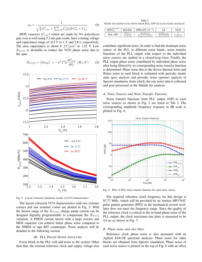
Fig. 5. Layout extracted simulation results of VCO characteristics.
The layout extracted VCO characteristics with two extremecorners and one nominal corner are plotted in Fig. 5. Withthe known range of the KV CO, charge pump current can bedesigned digitally programmable to compensate the KV CO
variation. A PMOS current mirror with a large resistor andMOS capacitor can achieve better phase noise compared tothe NMOS or npn BJT counterpart. Noise analysis will bedetailed in the following section.
III. PLL PHASE NOISE ANALYSIS
Every block in the PLL will add noise to the system. Otherthan that, the external reference clock and supply voltage also
Table INOISE TRANSFER FUNCTIONS FROM PLL O/P TO EACH NOISE SOURCES.
NTF|nO/Pns Ref+Div PFD+CP (A−1) LF VCO
PLL O/P NL(s)1+L(s)
2πNL(s)ICP (1+L(s))
2πKV COs(1+L(s))
11+L(s)
contribute significant noise. In order to find the dominant noisesource of the PLL at different noise bands, noise transferfunctions of the PLL output with respect to the individualnoise sources are studied in a closed-loop form. Finally, thePLL output phase noise contributed by individual phase noiseafter being filtered by its corresponding noise transfer functionis determined. Phase noise due to the device thermal noise andflicker noise in each block is estimated with periodic steadystate (pss) analysis and periodic noise (pnoise) analysis inSpectre simulation, from which, the raw noise data is collectedand post processed in the Matlab for analysis.
A. Noise Sources and Noise Transfer Function
Noise transfer functions from PLL output (O/P) to eachnoise sources as shown in Fig. 2 are listed in Tab. I. Thecorresponding amplitude frequency response in dB scale isplotted in Fig. 6.
103
104
105
106
107
-100
-50
0
50
100
150
Freq (Hz)
|NT
F| (
dB)
Noise Transfer Functions
NTFref,div
NTFvco
NTFR
NTFCP
Fig. 6. Plots of PLL noise transfer function for each noise source.
The required reference clock frequency for this design is97.77 MHz, which will be provided by an Anritsu MP1763Cpulse pattern generator (PPG) as the mechanical crystal oscil-lator does not meet the frequency range. Since the quality ofthe reference clock is critical to the in-band phase noise of thePLL output, the clock maximum rms jitter is measured to be4.8 ps as shown in Fig. 7.
B. Phase noise and rms Jitter
Reference clock phase noise is also measured with anAgilent E4411B spectrum analyzer. Phase noise for otherblocks are obtained from Spectre simulation. Phase noise ofeach noise source is plotted on the top of Fig. 8 with an offset
KimberlyHOlling
Text Box
This is an author-produced, peer-reviewed version of this article. The final, definitive version of this document can be found online at 2015 IEEE Workshop on Microelectronics and Electron Devices, published by IEEE. Copyright restrictions may apply. doi: 10.1109/WMED.2015.7093690
Fig. 7. Measured rms jitter of a 97.77 MHz clock generated from AnritsuPPG with Agilent DSO90254A oscilloscope (signal BW=2.5 GHz, samplingrate=20GSa/s).
frequency range from 1 kHz to 10 MHz. The PLL output totalphase noise and phase noise sources introduced by each blockseen at the PLL output are plotted at the bottom of Fig. 8.It can be observed that the reference phase noise seen at theoutput dominates the total output phase noise at lower offsetfrequency range, and the VCO output phase noise becamedominate from 3 MHz out onwards.
(6) is used to calculate the rms jitter (variance) of the phasenoise PSD in the time domain [8].
σrms =1
2πfV CO
√∫ fstop
fstart
S(f)df (6)
The calculated rms jitter of the reference clock and the VCOfrom their phase noise profile from 1 kHz to 10 MHz offsetfrequency range is 4.99 ps and 120.13 ps, respectively. Therms jitter of the PLL output phase noise profile is 5.01 ps.This manifests that most of the VCO noise is filtered out, butthe reference clock still contributes significantly.
IV. CONCLUSION
This paper presents a complete loop stability analysis andnoise analysis method for a 12.5 GHz charge pump PLL. Thedesign and analysis method is applicable to other PLL designs.The PLL output noise is mostly contributed by the noiseintroduced from external reference clock and VCO, such thata carefully chosen reference clock and the design a low phasenoise VCO becomes important for overall PLL performance.
REFERENCES
[1] S. Balagopal, K. Zhu, and V. Saxena, “A 1 GS/s, 31 MHz BW, 76.3dB dynamic range, 34 mW CT-∆Σ ADC with 1.5 cycle quantizer delayand improved STF,” Analog Integrated Circuits and Signal Processing,vol. 78, no. 2, pp. 275–286, 2014.
[2] K. Zhu, S. Balagopal, V. Saxena, and W. Kuang, “Design of a 10-Gb/sintegrated limiting receiver for silicon photonics interconnects,” in Proc.IEEE MWSCAS, Aug 2013, pp. 713–716.
103
104
105
106
107
-220
-200
-180
-160
-140
-120
-100
-80
-60
-40
-20
Offset Freq. (Hz)
SSB
Pha
se N
oise
(dB
c/H
z)
Noise Sources in the PLL
S
Φref
SΦ
div
SiCP
SvR
SΦ
vco
103
104
105
106
107
-160
-140
-120
-100
-80
-60
-40
Offset Freq. (Hz)
SSB
Pha
se N
oise
(dB
c/H
z)
SSB Output Phase Noise
SΦ
out
Total SΦ
out
Φref S
Φout
Φdiv S
Φout
iCP S
Φout
vR S
Φout
Φvco
Fig. 8. Phase noise of each noise source introduced into the PLL (top) andPLL output noise due to individual noise sources (bottom). Reference clockphase noise is the measured result. Other phase noise sources are obtainedfrom simulation.
[3] K. Zhu, V. Saxena, and W. Kuang, “Compact Verilog-A modeling ofsilicon traveling-wave modulator for hybrid CMOS photonic circuitdesign,” in Proc. IEEE MWSCAS, Aug 2014, pp. 615–618.
[4] K. Zhu, V. Saxena, X. Wu, and W. Kuang, “Design Considerations forTraveling-Wave Modulator Based CMOS Photonic Transmitters,” IEEETrans. Circuits Syst. II, Exp. Briefs, vol. 62, no. 4, pp. 412–416, 2015.
[5] T. Tokairin, M. Okada, M. Kitsunezuka, T. Maeda, and M. Fukaishi,“A 2.1-to-2.8-GHz Low-Phase-Noise All-Digital Frequency SynthesizerWith a Time-Windowed Time-to-Digital Converter,” IEEE J. Solid-StateCircuits, vol. 45, no. 12, pp. 2582–2590, Dec 2010.
[6] M. H. Perrott, “PLL design using the PLL Design Assistant program,”Microsystems Technology Laboratories, Massachusetts Institute of Tech-nology),(Apr. 2, 2005), vol. 33, 2002.
[7] B. Razavi, Design of Analog CMOS Integrated Circuits. McGraw-Hil,2000, pp. 326–334.
[8] W. Kester, “Converting oscillator phase noise to time jitter,” AnalogDevices, Application Note MT-008, 2008.
KimberlyHOlling
Text Box
This is an author-produced, peer-reviewed version of this article. The final, definitive version of this document can be found online at 2015 IEEE Workshop on Microelectronics and Electron Devices, published by IEEE. Copyright restrictions may apply. doi: 10.1109/WMED.2015.7093690


![SiGe BiCMOS for Analog, High-Speed Digital and Millimetre ...tcc/bctm_06_sv.pdf · BiCMOS process development [1]-[3]. While SiGe HBT performance has steadily improved over the last](https://static.documents.pub/doc/80x56/5ea16431fda46c45b810fb45/sige-bicmos-for-analog-high-speed-digital-and-millimetre-tccbctm06svpdf.jpg)
