Universiteit van Amsterdam Coherent Excitation of Rydberg Atoms on an Atom Chip Rutger M. T. Thijssen supervisor dr. R. J. C. Spreeuw December 2009 Master’s in Physical Sciences Quantum Atom Optics track Van der Waals–Zeeman Instituut Faculteit der Natuurwetenschappen, Wiskunde en Informatica Rydberg atoms, laser cooling, atom chip, electromagnetically induced transparency, atom–surface interaction
Transcript
Universiteit van Amsterdam
Coherent Excitation of RydbergAtoms on an Atom Chip
Rutger M. T. Thijssen
supervisordr. R. J. C. Spreeuw
December 2009Master’s in Physical SciencesQuantum Atom Optics track
Van der Waals–Zeeman InstituutFaculteit der Natuurwetenschappen, Wiskunde en
Informatica
Rydberg atoms, laser cooling, atom chip, electromagneticallyinduced transparency, atom–surface interaction
Abstract
Atom chips allow unprecedented flexibility in creating complex trapping poten-tials for neutral atoms, and construction of atom chips is facilitated by expertisein micro- and nanofabrication techniques from the semiconductor industry.
Highly excited Rydberg states of the trapped atoms could be used to mediatelong–range interactions between atoms trapped on the chip surface, for instancein the MAGCHIPS permanent magnetic lattice [1]. This could allow entangle-ment of mesoscopic ensembles of atoms, which paves the road toward quantuminformation processing with neutral atoms.
An open question is what effect the nearby surface has on the properties ofRydberg atoms.
To investigate this possible surface interaction we have built and characteriseda dedicated laser system using 780 nm and 480 nm narrow-band diode lasers.The 480 nm laser is stabilised to a two-photon electromagnetically inducedtransparency resonance in a rubidium vapour cell. We can excite Rydberg statesfrom n=19 up to n≈100. We have used this system to excite and image Rydbergatoms in an ultracold rubidium gas confined in a surface magneto–optical trap.
This thesis presents data on Rydberg–surface interaction measurements atdistances down to 50µm and Rydberg states up to |38d〉, finding no strongsurface interaction in this regime. This opens up possibilities for using Rydbergstates in atoms trapped near chip surfaces.
This master’s thesis describes an experiment carried out in the Quantum Gases& Quantum Information group at the Van der Waals–Zeeman Institute at theUniversity of Amsterdam. This introduction will give a short overview of thecontext in which this experiment was performed, a description of the experiment,and a short outline of the structure of the remainder of this report.
Cold Atoms and Atom Chips
One of the central issues in achieving the goal of a quantum computer is thatof scalability. In ion-trapping schemes, microfabricated-chip traps have beenshown to trap several ions and move them between different sites on the chip.
Neutral atoms have a significant advantage: they have intrinsically weak en-vironmental interactions. Nonetheless, they are routinely manipulated usingoptical and magnetic trapping techniques. The main tool to create large regis-ters of neutral atoms has been the optical lattice, which can create near perfectarrays of atoms with an atom separation of half the wavelength of the laser usedto create the trapping potential. However, achieving the resolution to addressindividual sites using optical techniques is still challenging.
Magnetic microtraps on atom chips are a promising alternative to optical lat-tices. An atom chip usually consists of a microscopic pattern of current-carryingwires, or permanent magnets arranged on a substrate to create complex cus-tomised trapping potentials. Encoding qubits in ground-state hyperfine levelson atom chips allows for very long coherence times [2].
Well-characterised micro- and nano-fabrication techniques make it feasible toscale up the number of microtraps on a single chip. One–dimensional potentialarrays and small arrays of several traps have been shown using both current-carrying wires and permanent magnets. The MAGCHIPS atom chip, on whichthis experiment was performed, greatly increases this previous work by creatinga two-dimensional magnetic lattice with more than 500 atom clouds, which areindividually optically resolvable [1].
Rydberg–Surface Interactions
A next step is to engineer interactions between atoms in different microtraps.Neutral atoms have weak interactions: this is why long coherence times areachievable. There are however several proposals to make separated neutralatoms interact. One of the most promising tools for mediating neutral atominteractions are Rydberg interactions. These have been demonstrated in free
v
vi INTRODUCTION
space: using dipole blockade effects [3], entangled mesoscopic qubits [4] and aCNOT gate between two atoms held in optical tweezers [5] have been produced.
The very fact that makes using Rydberg atoms interesting, their strong in-teractions, could make using them in an atom chip environment difficult. Typ-ically, the distance between microtraps is comparable to the distance betweenthe atoms and the chip surface. In our experiment, the lattice spacing is 22µm,and a typical height above the surface is 10µm. Therefore, the Rydberg atomscould very well have interactions with the surface, which is conducting, magneticand hot, of strengths comparable to Rydberg–Rydberg interaction strengths.
Atom–surface interactions have been studied before, and some limitations fortrapping ground–state neutral atoms are known [6]. These are limited mainlyby magnetic noise, which alters the trapping geometry or induces spin–flips.
Ion-trapping groups have also studied ion–surface interactions, with the in-teraction being between the ion and the electrode(s) creating the trapping po-tential. In this case, patch fields emanating from the electrodes proved to be alimiting factor [7].
While Rydberg atoms should be relatively robust against magnetic noise,with a loss comparable to that for ground–state atoms, the patch field effects,while weaker than in ion–trapping experiments, could still be strong enough toadversely affect trapping near the surface.
Experimental outline
To investigate the open question of the strength and source of Rydberg–surfaceinteractions, we have built a laser system to excite Rydberg atoms. This lasersystem, described in chapter 3, consists of two probe lasers at 780nm and a newhigh–power 480nm coupling laser. The probe lasers are frequency stabilisedusing polarisation spectroscopy, and considerable effort has been expended toensure narrow linewidths.
To frequency–stabilise the coupling laser used to excite from the intermediate|5p〉 state to the Rydberg states, we have implemented the novel technique ofexcited-state electromagnetically induced transparency (EIT), first shown in theAdams group in Durham [8].
We have also created a spatially–resolved imaging system to image Rydbergatoms near the chip surface. This imaging system again uses electromagnet-ically induced transparency. This is done to eliminate the complexity of field-ionization and charged–particle detectors from our system, while allowing us touse the familiar technique of resonant absorption imaging.
Chapters 1 and 2 describe the theory needed for this experiment, with chap-ter 1 describing electromagnetically induced transparency, including EIT in aDoppler-broadened medium, which is needed for the frequency stabilisation ofthe coupling laser. Chapter 2 derives several Rydberg–surface interactions, suchas near field blackbody radiation, patch–field heating and the effect of adsor-bates on the chip surface, and shows a technique to calculate Rydberg transitionwavelengths for setting the frequency of the coupling laser.
Chapter 3 describes the laser setup built for this experiment, including linewidthmeasurements on the 780nm probe laser system and a characterisation of ournew coupling laser.
Chapter 4 shows how Rydberg–surface interactions are measured in our sys-tem. This chapter also shows the experimental results, and discusses these.
Chapter 1
ElectromagneticallyInduced Transparency
In this experiment, electromagnetically induced transparency (EIT) is usedtwice: to frequency stabilise the coupling laser (section 3.4) and to image Ryd-berg atoms near the atom chip (section 4.2). It is therefore important to haveboth an understanding of the concept of EIT and the ability to calculate some ofits properties. This chapter will first decribe electromagnetically induced trans-parency in a qualitative fashion, outlining the effects of EIT [9, 10]. Secondly,the model we use to describe EIT in our experiment will be derived, using pa-rameters relevant for the experiment under consideration in this report. Afterthis, the model will be expanded to make it applicable to Doppler-broadenedsystems. This is done to describe EIT as it is used in stabilising our couplinglaser, where we observe electromagnetically induced transparency in a vapourcell heated to ∼70C.
1.1 EIT interpretation
Two quantum-mechanical pathways connecting the same levels interfere. Itis this interference that cancels the absorption in electromagnetically inducedtransparency. To achieve this EIT, we need a 3-level system. We (strongly)couple two of the levels to create two dressed states1 as shown on the right sideof fig. 1.1. This is done by using a strong coupling laser field. The splitting instates |5p〉 and |nd〉 is then an Autler-Townes doublet, caused by the AC Starkeffect. The size of the splitting is equal to the Rabi frequency of the couplinglaser. The transition probability amplitudes to these two dressed states fromthe third state in our system are opposite in sign and therefore cancel eachother [11].The spectral width of the transparency feature is not limited by the linewidth
of the probe transition (Γp), but only by the linewidth and Rabi frequency of
1A second, equally valid, interpretation is that of interfering pathways. The decayingstate, and therefore the absorbing state, in our system is the |5p〉 state. In the presence ofa strong coupling field, there are two ways to excite an atom to this state: |5s〉 → |5p〉, butalso |5s〉 → |5p〉 → |nd〉 → |5p〉. If both fields are on resonance, these pathways interferedestructively, causing a transparency in the absorption.
1
2 CHAPTER 1. THEORY OF EIT
autler-townes splitting+
fano-interference
not dressed dressed
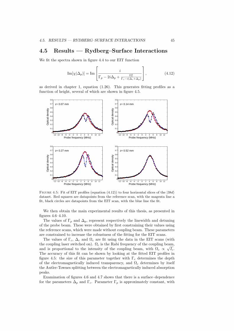
Figure 1.1: (a) The level scheme as used in our experiments, along with the relevantparamaters. (b) The level scheme in the dressed-state representation.
the coupling transition (Γc and Ωc respectively). This allows us to see effectsthat are much narrower than the rubidium D2 linewidth of 6.09 MHz [12]. Thisdoes require that the linewidth Γc is small. Because we use EIT in a ladderscheme, this linewidth includes not only the coupling laser linewidth, but alsothe inverse lifetime of the excited state we couple to. Rydberg states, whichhave a very long lifetime, meet this condition.
1.2 EIT modelling
We will model EIT using a density matrix approach. As a first step, the densitymatrix formalism, including the von Neumann operator, will be derived. Wewill then introduce the Hamiltonian describing our system. After introducingthis Hamiltonian, we will show how the coupling laser creates dressed states of|5p〉 and |nd〉. After showing the effects of the Autler-Townes doublet that iscreated, we will solve the von Neumann equation and derive an expression forthe susceptibility of the atoms to the probe beam.
Density Matrix
Pure quantum states are described by wavefunctions that are solutions to theSchrodinger equation:
i~∂
∂t|ψ〉 = H|ψ〉. (1.1)
Using the Schrodinger equation requires knowledge of the form of the wavefunc-tions. The Schrodinger equation also requires a description of the full system,including the reservoir that accommodates dissipation, and does not allow fordescription of mixed states. We will therefore describe our systems in terms ofdensity matrices.
1.2. EIT MODELLING 3
The density matrix allows us to describe systems where the exact form of thewavefunctions |ψ〉 is not known, but only the distribution Pψ over the wave-functions is known. The density matrix can then be defined as
ρ =∑ψ
Pψ|ψ〉〈ψ|. (1.2)
Using the density matrix formalism also allows us to reduce the system we study.In our system, the wavefunctions would include not only the states of the atoms,but also of all the photons involved. When using density matrices, it is easy torestrict the calculations to subsections of the complete system. If a system is ina state
ρtot = ρ1ρ2, (1.3)
where ρ1 and ρ2 are density matrices describing a portion of the system, we canreduce the density matrix to ρ1 by calculating the trace over ρ2:
ρ1 = Tr2ρtot. (1.4)
The time evolution of the density matrix is described by the von Neumannequation. This equation is easily derived by taking the time derivative of thedensity matrix operator ρ,
ρ =∑ψ
Pψ(|ψ〉〈ψ|+ |ψ〉〈ψ|), (1.5)
and then using the Schrodinger equation
˙|ψ〉 = − i~H|ψ〉. (1.6)
to replace 〈ψ| and |ψ〉 in equation (1.5). This results in:
ρ =∑ψ
Pψ
(− i
~H|ψ〉〈ψ|+ |ψ〉〈ψ|H i
~
)(1.7)
= − i~
H∑ψ
Pψ|ψ〉〈ψ| −∑ψ
Pψ|ψ〉〈ψ| · H
(1.8)
= − i~
[H, ρ] (1.9)
with [H, ρ] the commutator Hρ − ρH. We now introduce a Hamiltonian de-scribing the couplings and detunings of the two laser fields. To simplify thenotations, atomic transition operators are used, with σij = |i〉〈j|. The inter-action Hamiltonian is then, following [13], in the rotating frame and using therotating wave approximation,
Hint = −~2
[Ωp(t)σ21ei∆pt + Ωc(t)σ32e
i∆ct + H.c.], (1.10)
with Ωp(t) and Ωc(t) the Rabi frequencies of the probe and coupling laser fields,and ∆p and ∆c the probe and coupling detunings, as shown in figure 1.1.This produces a matrix for the Hamiltonian:
H =~2
2∆p Ωp 0Ωp 0 Ωc0 Ωc −2∆c
(1.11)
4 CHAPTER 1. THEORY OF EIT
1.3 Dressed States
We can look at the 2× 2 submatrix of the Hamiltonian, describing the |5p〉 and|nd〉 states, and solving this using the dressed state formalism, which is derivedin Appendix A. The submatrix is then
H =~2
(∆c ΩcΩc ∆c
), (1.12)
Solving this for eigenvalues we obtain
~Ω = ±~√
∆2c + Ω2
c , (1.13)
with two dressed states
|+〉 = sin θ|nd,N〉+ cos θ|5p,N − 1〉 (1.14)|−〉 = cos θ|nd,N〉 − sin θ|5p,N − 1〉 (1.15)
with mixing angle θ defined as
tan 2θ = −Ωc∆c
; 0 ≤ 2θ ≤ π (1.16)
If we set ∆c = 0, the resonant limit is obtained. Then tan 2θ = Ωc/0, whichhas a solution for θ = π/4. In this limit, the splitting between the two dressedstates is given by Ωc, the coupling Rabi frequency. The dressed states can thenbe rewritten as
|+〉 =1√2
(|nd〉+ |5p〉) (1.17)
|−〉 =1√2
(|nd〉 − |5p〉) (1.18)
This situation is shown in figure A.1(b) and the right–hand side of figure 1.1.We are interested in the transition probability from the |5s〉 ground state.
Neglecting the decay from the |nd〉 Rydberg state, the contributions to thetransition probability from |5s〉 to the non-dressed level |5p〉 cancel, because theyhave the opposite sign. This produces a total transparency on the |5s〉 ↔ |5p〉transition. The next section will show how this total transparency is modifiedby decay of the excited states.
1.4 Spontaneous emission and collisions
After showing a simplified picture of electromagnetically induced transparency,we will show the derivation we have used to generate absorption profiles. We re-turn to our 3×3 density matrix, and calculate the time dependence of ρ(t) usingthe von Neumann equation. Spontaneous emission and collisional broadeningare added into the model using the Lindblad superoperator. The von Neumannequation and Lindblad superoperator are given by:
ρ = − i~
[H, ρ] + L (1.19)
L = γ
(σρσ† − 1
2(σ†σρ+ ρσ†σ)
), (1.20)
1.4. SPONTANEOUS EMISSION AND COLLISIONS 5
where the Lindblad operator can also be written as:
L = γ(σρσ†)− γ
2ρ, σ†σ (1.21)
with σ = σij atomic interaction operators and ρ, σ†σ = ρσ†σ + σ†σρ theanti-commutator of ρ and σ†σ. We define two spontaneous emission Lindbladoperators as follows:
Γc : Γc[σ31ρσ13 −12
(σ33ρ+ ρσ33)] (1.22)
Γp : Γp[σ21ρσ12 −12
(σ22ρ+ ρσ22)] (1.23)
Which produces a matrix operator for spontaneous emission: Γpρ22 − 12Γpρ12 − 1
2ρ13Γc− 1
2Γpρ21 −Γpρ22 + Γcρ33 − 12 (Γp + Γc)ρ23
− 12Γcρ31 − 1
2 (Γp + Γc)ρ32 −Γcρ33
(1.24)
We can construct a similar matrix for collisional decay. We can write a Lindbladmatrix operator for collision-induced decay as 0 −2γc1ρ12 −2(γc1 + γc2)ρ13
−2γc1ρ21 0 −2γc2ρ23
−2(γc1 + γc2)ρ31 −2γc2ρ32 0
(1.25)
We can then calculate the total matrix ρ by adding the von Neumann operator(1.19) to the two Lindblad operators (1.24) and (1.25). Mathematica is thenused to solve this equation analytically.
Finally, after finding the steady-state solution to this density matrix equation,we can take the first-order expansion in probe power, Ωp Ωc, to get anexpression for the susceptibility on the probe transition, which is proportionalto ρ21. This first-order expansion is valid because we will use weak probe beamsto avoid populating the |5p〉 state. The susceptibility is then given by:
χ(∆p) =i
Γp − 2i∆p + Ω2c
Γc−i(∆c+∆p)
. (1.26)
This susceptibility is a complex number. The real part Re[χ] determines therefractive index. This can be negative and have a very high slope in the EITregime, leading to ultraslow group velocities. These effects will not be discussedfurther, for more information see [10, 13]. The imaginary part Im[χ] determinesthe absorption, which is what we are interested in. Note that in this first-ordersusceptibility there is no contribution from collisional decay. If we set Ωc = 0,the equation should reduce to the normal 87Rb D2 absorption profile. Theequation becomes
χ(∆p,Ωc = 0) =i
Γp − 2i∆p, (1.27)
the imaginary part of which is a Lorentzian absorption profile, defining Γp asthe full width at half maximum:
Abs =Γp
Γ2p + 4∆2
p
(1.28)
6 CHAPTER 1. THEORY OF EIT
-10 -5 0 5 100.0
0.2
0.4
0.6
0.8
1.0
Probe detuning Dp @MHzD
OD
Wc= 0
Wc= 3MHz
Figure 1.2: Theoretical EIT absorption profiles. The red line has no coupling, theblue line has coupling. Parameters are: Γp = 2π × 6 MHz, Γc = 2π × 0.06 MHz,Ωc = 2π × 3 MHz, ∆c = 0.
1.5 EIT in Doppler-broadened media
For ultracold atoms, Doppler broadening is negligible. For our EIT locking,which is done in a heated vapour cell, this is not the case. We use a counterprop-agating geometry to reduce Doppler broadening, but because of the wavelengthmismatch between the probe (780nm) and coupling (480nm) beams we cannoteliminate it completely.We can however calculate a spectrum for EIT in a Doppler-broadened medium,as shown in [14, 15]. The EIT absorption function, formula (1.26), derivedin section 1.2, can be modified to include Doppler effects. The detunings inthis equation are modified to include Doppler broadening by remembering that∆p = ωp − ω21. Atoms moving at a speed v towards the probe beam then seethe probe light upshifted by ωpv/c. These atoms, which are moving with thecoupling beem in our counterpropagating setup, see the coupling light down-shifted by −ωcv/c. This allows us to modify our susceptibility expression (1.26)to:
χ(∆p, v) =i
Γp − 2i∆p − 2iωp
c v + Ω2c
Γc−i(∆p+∆c)−i(ωp−ωc)v/c
N(v), (1.29)
where N(v) is the atomic velocity distribution. By assuming a Maxwellianvelocity distribution, so that
N(v) =N0
u√πe−v
2/u2, (1.30)
with |u|/√
2 the root-mean-square atomic velocity, which we can calculate to be
u/√
2 =
√kBT
M, (1.31)
as a function of the vapour cell temperature in Kelvin, with kB Boltzmann’sconstant and M the mass of a rubidium–87 atom. Taking the imaginary part
1.5. EIT IN DOPPLER-BROADENED MEDIA 7
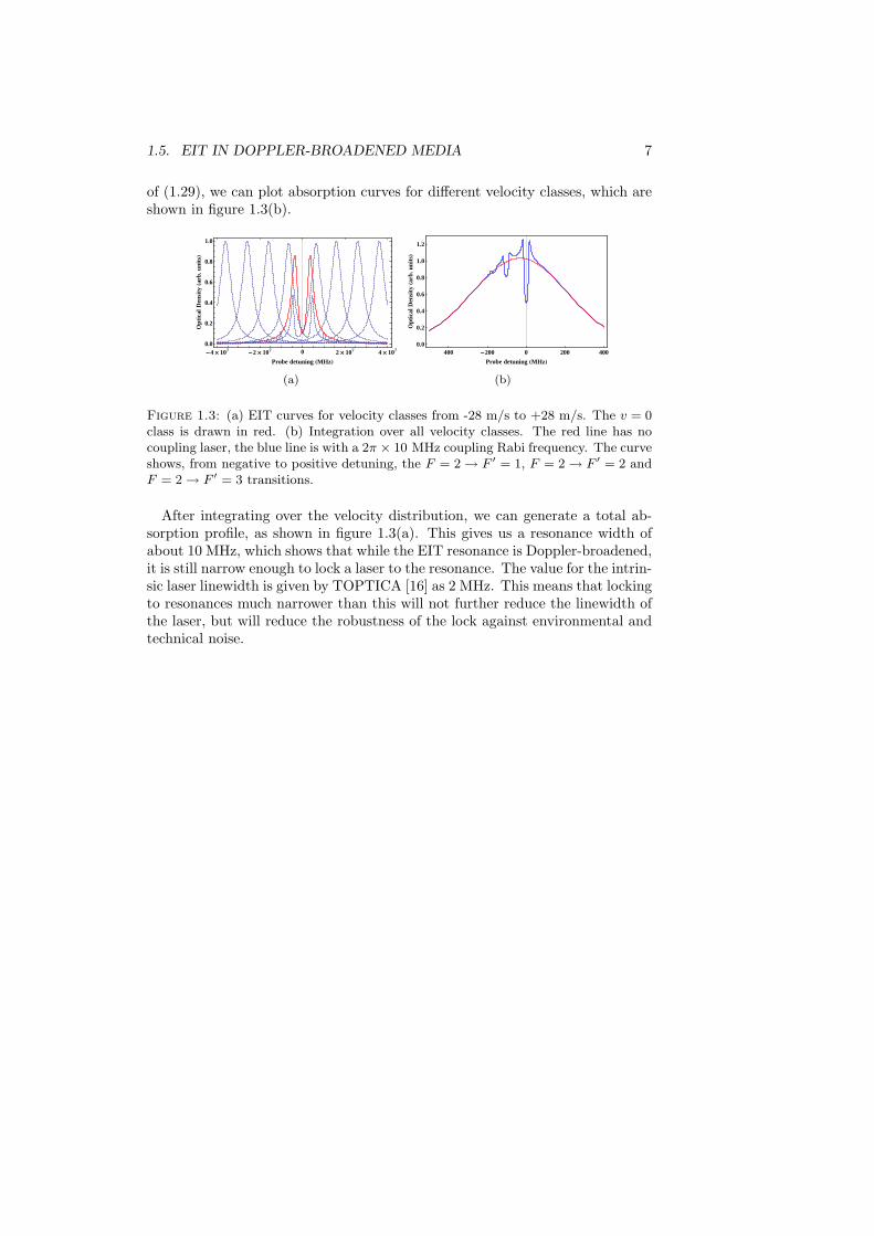
of (1.29), we can plot absorption curves for different velocity classes, which areshown in figure 1.3(b).
-4 ´ 107 -2 ´ 107 0 2 ´ 107 4 ´ 1070.0
0.2
0.4
0.6
0.8
1.0
Probe detuning HMHzL
Opt
ical
Den
sity
Harb
.uni
tsL
(a)
400 -200 0 200 4000.0
0.2
0.4
0.6
0.8
1.0
1.2
Probe detuning HMHzL
Opt
ical
Den
sity
Harb
.uni
tsL
(b)
Figure 1.3: (a) EIT curves for velocity classes from -28 m/s to +28 m/s. The v = 0class is drawn in red. (b) Integration over all velocity classes. The red line has nocoupling laser, the blue line is with a 2π × 10 MHz coupling Rabi frequency. The curveshows, from negative to positive detuning, the F = 2→ F ′ = 1, F = 2→ F ′ = 2 andF = 2→ F ′ = 3 transitions.
After integrating over the velocity distribution, we can generate a total ab-sorption profile, as shown in figure 1.3(a). This gives us a resonance width ofabout 10 MHz, which shows that while the EIT resonance is Doppler-broadened,it is still narrow enough to lock a laser to the resonance. The value for the intrin-sic laser linewidth is given by TOPTICA [16] as 2 MHz. This means that lockingto resonances much narrower than this will not further reduce the linewidth ofthe laser, but will reduce the robustness of the lock against environmental andtechnical noise.
8 CHAPTER 1. THEORY OF EIT
Chapter 2
Theory of Rydberg–SurfaceInteractions
This experiment aims to show how Rydberg atoms interact with a surface. Topredict some of these effects, it is helpful to know some of the properties ofRydberg atoms. This chapter will give a brief description of Rydberg atoms,and present the methods used to calculate the transition wavelengths for theRydberg series in 87Rb (section 2.2). We will then investigate possible Rydberg-surface interactions (section 2.3), and give a description of Rydberg-Rydbergatoms, in the form of Van der Waals dipole-dipole interactions and Forsterresonances (section 2.4).
2.1 Properties of Rydberg atoms
Figure 2.1: Sketch of a Rydberg atom: one highly excited electron orbiting an ioniccore
For rubidium, there is no analytical solution for the Schrodinger equation,because there are more than two particles involved: a nucleus with a +37 chargeand 37 electrons.
However, for highly excited electronic states, the Rydberg states, there is avery good semi-classical approach [17] that describes many atomic propertieswithout having to solve the full Schrodinger equation. The state of the atom isdescribed by the state of the highly–excited outer electron. This spends most ofits time far from the core and the other 36 electrons, which together are referredto as the ‘ionic’ core. It is therefore possible to approximate the ionic core as apoint particle with a +1 charge: all but one of the +e charges of the nucleus areshielded by the inner electrons. We can then calculate the motion of the outer
9
10 CHAPTER 2. THEORY OF RYDBERG–SURFACE INTERACTIONS
electron in the 1/r potential of the ionic core. This generates Kepler orbits(figure 2.1), with the long axis of the orbit determined by the energy of thestate, scaling as n2, and the short axis determined by the angular momentumquantum number `. The Kepler equation can be solved numerically, and allowsthe calculation of many of the properties of Rydberg atoms. Some propertiesof Rydberg atoms are shown in table 2.1.
Property n dependence value for Rb |43s〉Binding energy n−2 8.56meVEnergy between adjacent n states n−3 109.66 GHzOrbital radius n2 2384.2a0
Geometric cross section n4 1.78 · 107a20
Dipole moment 〈nd|er|nf〉 n7 −105.16 a.u.Dipole moment 〈5p|er|ns〉 n−1.5 −0.0176 a.u.Polarizability n7 8.06 MHz/(V/cm)2
Table 2.1: Some properties of Rydberg atoms, data from [17, 18].
High ` states are always far from the core, and the n-dependencies given intable 2.1 are accurate. This is not true for low ` states: they penetrate into theionic core: this reduces the shielding by the 36 inner electrons, making themfeel a higher nuclear charge. This causes a deviation from the Coulombic 1/rpotential. The net effect is to lift the `-degeneracy of the atomic states. Amodification to the potential must be made. This is done using a procedureknown as Quantum Defect Theory. In this approach, the energy of the Rydbergstates is calculated by
En` = − RM(n− δn,`)2
, (2.1)
introducing a ‘quantum defect’, δn,`, and where RM is the reduced Rydbergconstant, as a function of R∞,
RM =R∞
1 +me/M; R∞ =
mee4
8ε20h3c
with R∞ the Rydberg constant for an infinitely heavy core, me, the electronmass, and M , the mass of the 87Rb core. The quantum defect, δn,`, is an ex-perimentally obtained parameter. The quantum defects used in this calculationwere obtained from [19]. To make the scalings given in table 2.1 accurate forlow-` states, the n-values in the table must be replaced with n∗ = n− δn,`.
2.2 Calculating Rydberg series using QuantumDefect Theory
A notebook was written in Mathematica to calculate tables of Rydberg energiesand the expected energy splittings between the |nd3/2〉 and |nd5/2〉 fine-structure
2.3. SURFACE EFFECTS 11
states. The wavelength is calculated using the Rydberg formula, as
λRyd(n, l) =1
ion.pot.− RM(n−δn,`)2 −D2
, (2.2)
where ion. pot. is the ionisation potential, 33 690.804 cm−1 (=296.8nm), RMis the reduced Rydberg constant, and D2 is the energy difference between the|5s〉 and |5p〉 states. A list of Rydberg states calculated using this formula isshown in table 2.2.
2.3 Surface effects
This section will describe the interactions that could couple the Rydberg atomsto the chip surface, including near field blackbody radiation, patch field radia-tion and the effects of adsorbates.
2.3.1 Spontaneous emission and blackbody radiation
Before introducing near-field effects, it is useful to discuss the loss processes forexcited Rydberg atoms in free space. In free space, there are two loss processes:spontaneous emission and blackbody radiation induced loss.We will define a blackbody spectral energy density as
SbbE (ω) =~ω3
3πε0c3(nth + 1), (2.3)
where nth is the Boltzmann distribution, given by
nth =1
e~ω/kBT − 1(2.4)
and the vacuum field is given by the +1 term in the energy density function.This +1 term causes spontaneous emission. Because of the ω3 in this function,spontaneous emission favours transitions with high frequencies. For the Ryd-berg series, these are transitions back to the ground state. Because we will bestudying |ns〉 and |nd〉 states, the highest energy dipole–allowed transitions arethose from the Rydberg state down to |5p〉. Gallager [17] gives a function forthis rate as
1τ
=1
τ0(n∗)α, (2.5)
where τ0 and α are experimental parameters, and n∗ is the principal quantumnumber n minus the quantum defect δ. For |ns〉 states, τ0 is 1.43 ns and α is2.94, while for |nd〉 states, τ0 is 2.09 ns and α is 2.85.
2.3.2 Blackbody decay
A non-zero temperature introduces nonzero occupation values in the Boltzmanndistribution. For the spontaneous-emission transitions, the Boltzmann distribu-tion gives a thermal occupation that is practically 0. However, for transitionsbetween Rydberg states, there is a significant thermal occupation of modes. The
12 CHAPTER 2. THEORY OF RYDBERG–SURFACE INTERACTIONS
n ` λc [nm] 2λ [nm] d–splitting [MHz]19 d 487.278 974.557 1393.5121 s 487.079 974.15820 d 486.408 972.815 1202.0522 s 486.239 972.47821 d 485.669 971.338 1044.0723 s 485.525 971.0522 d 485.037 970.073 912.55924 s 484.913 969.82523 d 484.491 968.982 802.21525 s 484.384 968.76724 d 484.017 968.035 708.94626 s 483.923 967.84725 d 483.603 967.206 629.57727 s 483.521 967.04126 d 483.239 966.478 561.61628 s 483.166 966.33227 d 482.917 965.834 503.08629 s 482.852 965.70428 d 482.631 965.261 452.40730 s 482.573 965.14629 d 482.375 964.75 408.30831 s 482.324 964.64730 d 482.146 964.293 369.75432 s 482.1 964.231 d 481.94 963.881 335.90233 s 481.899 963.79732 d 481.754 963.509 306.05734 s 481.717 963.43333 d 481.586 963.172 279.64335 s 481.552 963.10334 d 481.433 962.865 256.18236 s 481.401 962.80335 d 481.293 962.586 235.27237 s 481.265 962.52936 d 481.165 962.331 216.57538 s 481.139 962.27937 d 481.048 962.097 199.80839 s 481.024 962.04938 d 480.941 961.882 184.72640 s 480.919 961.838
Table 2.2: Calculated |5p〉 → |n`〉 Rydberg transitions. The 2λ column is includedfor ease in setting the laser diode frequency on the TA–SHG coupling laser. Thed–splitting column shows the fine–structure spacing between the |nd3/2〉and |nd5/2〉states.
2.3. SURFACE EFFECTS 13
strongest blackbody–induced Rydberg–Rydberg transitions for our experimentare the following:
|ns〉 → |np〉|(n− 1)p〉
|nd〉 → |(n+ 1)p〉|(n− 1)f〉
We can use equation (2.2) shown in section 2 to calculate frequencies for thesetransitions. Figure 2.2 shows the frequencies for Rydberg blackbody transi-tions for |nd〉 states. The |ns〉 blackbody transitions have similar transitionfrequencies, and are not shown. We can then compare these frequencies to the
20 30 40 50 60 70 80
1 1010
2 1010
5 1010
1 1011
2 1011
Principal quantum number n
FrequencyHz
Figure 2.2: Rydberg blackbody transition frequencies. The red circles are transitionfrequencies for |nd〉 → |(n−1)p〉 transitions, the blue squares are for |nd〉 → |(n+1)f〉transitions.
Boltzmann spectrum given in equation (2.3), which is shown in figure 2.3.If ω kBT/~, which at T = 300 K translates to ω 4 × 10¹³Hz, we can
approximate nth asnth ≈ kBT/~ω. (2.6)
It is apparent that the approximation given above is valid for the Rydberg–Rydberg transitions. The transition rate should scale as the spontaneous emis-sion rate, multiplied by 1/ω, which originates from equation (2.6). This impliesthat where the spontaneous emission rate scales with the principle quantumnumber as n−3, the blackbody rate will scale as n−2.
In the following discussion, to simplify calculations, we will only considerone of the blackbody decay channels, and make a correction to the dipole ma-trix elements to obtain the same result as in the approximate formula given inGallagher’s (5.16)1:
1τbbnl
=4αkBT3~n∗2
. (2.7)
1Gallagher uses atomic units, where this thesis uses SI units. Where appropriate, formulashave been converted to SI.
14 CHAPTER 2. THEORY OF RYDBERG–SURFACE INTERACTIONS
109 1010 1011 1012 1013 1014 101510-18
10-16
10-14
10-12
10-10
10-8
Frequency @HzD
SE
@V2 m
-2 s-
1 D
Figure 2.3: Boltzmann spectrum for T = 300 K. The red shaded area indicates theRydberg–Rydberg transitions shown in figure 2.2, the blue shaded region indicates the|Ryd〉 → |5p〉 transition. The dashed lines show the near field energy spectrum at 10µm (green), 20 µm (yellow) and 50 µm (red) from a gold surface.
It is clear that blackbody decay scales as n∗−2.To do a full derivation of the rates approximated in (2.5) and (2.7), we would
have to calculate the dipole matrix elements e2R(ω)2/~2 = 〈nlm|er|n′l′m′〉, inorder to perform the calculation
ΓBB+SE =1τSE
+1τBB
=∑ω
e2R(ω)2
~2SE(ω), (2.8)
summing over all possible transitions. We will not do this calculation here.However, it is useful to introduce this form, as it allows us to examine the effectof energy distributions other than the normal blackbody distribution.
2.3.3 Near field effects
One such different distribution is that of the blackbody field near a surface. Thefree-space blackbody components interact and reflect from conducting surfaces,giving a different energy distribution near this surface. This section will followthe derivation given by Henkel in [7]. We will calculate a near field effect basedon the atom chip surface used in MAGCHIPS [20], which features a top layerof 100nm of gold, over an FePt layer with a thickness of 300nm on a siliconsubstrate.
The main parameter in calculating near-field effects is the skin-depth. Thisis given by
δ(ω) =c
ω
√2ε0ρω, (2.9)
where ρ is the specific resistance. For gold, ρ = 0.02214× 10⁻⁶ Ωm. Because ofthe thinness of the layers on the atom chip in question, it is useful to plot theskin depth as a function of frequency, as is shown in figure 2.4. If we comparethis to figure 2.2, we can see that for the highest Rydberg states, the skin depth
2.3. SURFACE EFFECTS 15
is larger than the thickness of the gold layer on the MAGCHIPs atom chip.However, because our chip is not a thin film, but has an FePt layer and a Sisubstrate beneath the gold, we will assume that this will lead to a correctionthat we can neglect. A model for near-field effects near a thin film is given byHenkel in [21].
108 109 1010 1011 1012 1013 1014
1.00
0.50
5.00
0.10
0.05
0.01
frequency f @HzD
skin
dept
h@Μ
mD
Spiral
Figure 2.4: Skin depth of a gold surface as a function of frequency. The gray boxindicates the main transition frequencies for the Rydberg states and the thickness ofthe chip.
Henkel derives the near-field spectral density using Fresnel reflection coeffi-cients leading to a Green function describing the modification to the thermalradiation. He writes
S(nf)ijE (r, ω) = SbbE (ω)gij(kz), (2.10)
where i, j ∈ x, y, z. After calculating gij , an interpolation formula is given to be
gij(kz) =3δ2
8kz3
(sij + δij
z
δ(|ω|)
), (2.11)
which is valid both in the regime of large skin depth (the sij term) and smallskin depth (the δij zδ term). Note that in this equation, δ(|ω|) is the skin depth,while δij is the Kronecker delta. If we apply the high-temperature limit ofthe Boltmann distribution given in formula (2.6), we get an expression for thenear-field spectrum as
S(nf)ijE (r;ω) =
kBTρ
4πz3
(sij + δij
z
δ(|ω|)
). (2.12)
This spectral energy density is shown in the dashed lines in figure 2.3. In thisequation sij is a diagonal tensor with elements sxx = syy = 1
2 , szz = 1. However,this tensor only comes into play in the regime where z δ. As discussed earlier,the skin depth in the frequency range we are interested in is ≤ 1µm. Therefore,the contribution of this term can be neglected.
16 CHAPTER 2. THEORY OF RYDBERG–SURFACE INTERACTIONS
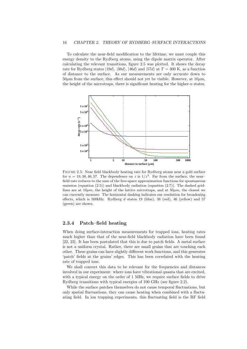
To calculate the near-field modification to the lifetime, we must couple thisenergy density to the Rydberg atoms, using the dipole matrix operator. Aftercalculating the relevant transitions, figure 2.5 was plotted. It shows the decayrate for Rydberg states |19d〉, |38d〉, |46d〉 and |57d〉 at T = 300 K, as a functionof distance to the surface. As our measurements are only accurate down to50µm from the surface, this effect should not yet be visible. However, at 10µm,the height of the microtraps, there is significant heating for the higher-n states.
1 5 10 50 100 500 1000
5 ´ 104
1 ´ 105
5 ´ 105
1 ´ 106
5 ´ 106
1 ´ 107
distance to surface @ΜmD
deca
yra
te@s-
1 D
Figure 2.5: Near field blackbody heating rate for Rydberg atoms near a gold surfacefor n = 19, 38, 46, 57. The dependence on z is 1/z2. Far from the surface, the near–field rate reduces to the sum of the free-space approximation functions for spontaneousemission (equation (2.5)) and blackbody radiation (equation (2.7)). The dashed grid-lines are at 10µm, the height of the lattice microtraps, and at 50µm, the closest wecan currently measure. The horizontal dashing indicates our resolution for broadeningeffects, which is 500kHz. Rydberg d–states 19 (blue), 38 (red), 46 (yellow) and 57(green) are shown.
2.3.4 Patch–field heating
When doing surface-interaction measurements for trapped ions, heating ratesmuch higher than that of the near-field blackbody radiation have been found[22, 23]. It has been postulated that this is due to patch fields. A metal surfaceis not a uniform crystal. Rather, there are small grains that are touching eachother. These grains can have slightly different work functions, and this generates‘patch’ fields at the grains’ edges. This has been correlated with the heatingrate of trapped ions.
We shall convert this data to be relevant for the frequencies and distancesinvolved in our experiment: where ions have vibrational quanta that are excited,with a typical energy on the order of 1 MHz, we require surface fields to driveRydberg transitions with typical energies of 100 GHz (see figure 2.2).
While the surface patches themselves do not cause temporal fluctuations, butonly spatial fluctuations, they can cause heating when combined with a fluctu-ating field. In ion trapping experiments, this fluctuating field is the RF field
2.3. SURFACE EFFECTS 17
used to trap the atoms. In our experiment, we argue that thermal dissipationin the chip causes temporally fluctuating patch fields.
The heating rate for a trapped ion is given by Deslauriers et al. in [22] as
˙n =e2
4M~ω2z
SpatchE (ωz) (2.13)
with SpatchE the spectral energy density of the patch field, and e2
4M~ω2z
the cou-pling of the ion to the radiation, with e the electron charge, M the mass of thetrapped ion and ωz the trap frequency. Epstein et al. in [23] show the heating
1 5 10 50 100 500104
105
106
107
108
109
1010
distance to surface @ΜmD
deca
yra
te@s-
1 D
Figure 2.6: Patch–field heating, using the scaling laws given by Epstein et al., forRydberg d–states 19 (blue), 38 (red), 46 (yellow) and 57 (green). The dashed linesindicate the near field blackbody heating for the same states.
rate for a large number of different ion trapping experiments, finding a scalingfor ˙n as
˙n ∼ ω−2.4z−4. (2.14)
We have then solved this for the experimental values given by Deslauriers et al.[22], to find
SpatchE (ωz) = α ˙n
4M~ω2z
e2(2.15)
with α a proportionality constant. The factor of ω that is in the coupling factorleads to an ω-dependence Spatch
E ∼ ω−1.4. To calculate the effect on Rydbergatoms near surfaces, we couple the Spatch
E (ω) to Rydberg transitions, using thedipole matrix operator e2R2/~2, giving
Γpatch =e2R2
~2SpatchE (ω). (2.16)
This is plotted in figure 2.6, together with the heating rate for near fieldblackbody radiation for Rydberg states d-states 19, 38, 46 and 57, showing thatpatch field heating is of a strength comparable to that of blackbody heating.
18 CHAPTER 2. THEORY OF RYDBERG–SURFACE INTERACTIONS
1 5 10 50 100 500104
105
106
107
108
109
1010
distance to surface @ΜmD
deca
yra
te@s-
1 D
Figure 2.7: Total decay rate: spontaneous emission, near field blackbody and patchheating. Rydberg d–states 19 (blue), 38 (red), 46 (yellow) and 57 (green) are shown.
However, because of the strong z-dependence, very close to the surface patch–field heating will be dominant.
Finally, figure 2.7 shows the effect of near field blackbody and patch–fieldheating added up.
2.3.5 Electric fields on chip: shifting of resonances
Diffusion in the chip, leading to patch fields, can not only cause transitions toneighbouring Rydberg states, but also shift the Rydberg energy levels. Rydbergstates are highly polarizable, and this leads to their energies shifting in electricfields. For the low ` states only the second-order Stark shift has an effect. Then
∆E = −12αF 2, (2.17)
with ∆E the energy shift, α the polarizability, which scales with n7, where Fis the electric field.
2.3.6 Rubidium adsorbates
There have been several experiments where Bose-Einstein condensates were usedto probe the effect of adsorbates on a chip surface on ground state atoms, seethe discussion in [24–26]. It is very difficult to extrapolate this to our currentexperiment: the data was very sensitive to the exact distribution of adsorbatesover the surface. In [27] a scaling is give at z−2.3 for a Si substrate and z−2 fora Ti substrate. This could be used to distinguish adsorbate effects from othereffects. [27] also discusses the removal of adsorbates from a surface, using eitherUV light or laser ablation. It appears that this is non–trivial, and would requirefurther research.
The chip surface not only has an effect on Rydberg states directly. Thecoupling laser we use has a relatively short wavelength, and therefore its photons
2.4. RYDBERG–RYDBERG INTERACTIONS 19
have a higher energy: the energy of a 480nm photon, in electronvolt, is
Eph =~cλ
= 2.583 eV (2.18)
This means that we must investigate the work function of the various materialsthat are on the surface. Our chip is coated in gold and has rubidium adsorbedto it from previous experimental runs. The work function for gold is between5.47 and 5.31 electronvolt, depending on the crystal orientation. For metallicrubidium the work function is 2.261 eV [28]. If we hit the chip surface with bluelaser light, we can photo-ionise adsorbed rubidium. This introduces charges,both rubidium ions and electrons, near our sensitive Rydberg atoms. Becausethese charges are free-flying they can pass the Rydberg atoms at arbitrarilyclose distances, generating extremely large electric fields, which could then notonly perturb the Rydberg atoms, but also ionise them, using the process offield-ionisation (for a discussion on field-ionisation of Rydberg atoms, see e.g.[29]).
The section on aligning the laser beams, section 4.2.1, discusses how we pre-vent the laser beam from hitting the surface, and what effects are visible whenthe blue laser does hit the chip surface.
2.3.7 Magnetic Effects
This chapter has not yet discussed the effects of nearby magnetic fields onRydberg atoms. This is because magnetic effects do not depend on the principalquantum number n. This implies that Rydberg atoms are magnetically similarto ground state atoms. The trapping lifetimes for ground state atoms in theMAGCHIPS lattice has been shown to be long enough, and limited more bybackground gas collisions than by magnetic surface noise. There are discussionsin the literature on surface magnetic noise and its effects on trapping lifetimes,see for instance [30].
2.4 Rydberg–Rydberg Interactions
The big advantage of Rydberg atoms is that there are strong Rydberg-Rydberginteractions. There are two main interaction types: Van der Waals interactions,leading to ‘dipole blockade’ and Forster resonances, which are longer ranged, andcan lead to resonant population transfer [31]. Both interactions are governedby the dipole interaction, which scales as Vdip ∼ n4/r3. We can then writea Hamiltonian for two interacting Rydberg atoms, with a basis formed by aninitial state |AA〉 and a final state |BC〉, where A,B and C are Rydberg states:
Hint =(
0 VdipVdip ∆
)(2.19)
where ∆ is the energy difference between the final and the initial state. In theregime Vdip ∆, the energy eigenstates scale as (Vdip)2/∆. As ∆ scales as n−3
(see table 2.1), the total interaction scales as n11/r6. This is the (nonresonant)Van der Waals interaction. For this interaction, the blockade radius is given asrb = ( C6
~Γc)1/6, where C6 is the Van der Waals C6 coefficient. This means that if
20 CHAPTER 2. THEORY OF RYDBERG–SURFACE INTERACTIONS
the combined transition linewidth Γc < ~Vdip, excitation of a second Rydbergatom is blocked.
If the Rydberg states are made resonant, for instance by applying a smallelectric field, the regime Vdip ∆ can be reached, and the interaction scales asVdip ∼ n4/r3, which is known as Forster resonance interaction.
2.4.1 Rydberg Self–interaction
Through the dipole blockade mechanism and a nearby surface, a Rydberg atomcould also interact with itself. The presence of the Rydberg atom with its dipolemoment near a surface could induce a charge distribution in the surface. TheRydberg atom can then interact with this charge distribution, using the methodof mirror-potentials. This effect would be very interesting to study, but we onlyexpect it on the length scale of the dipole blockade radius, which is on the orderof microns, and therefore well below the regime we will study in our experiment.
2.5 Scaling of Rydberg–Surface and Rydberg–Rydberg Interactions
It is useful at this point to compare Rydberg-surface and Rydberg-Rydberginteractions: we want to know if there is a regime in n, z and r where theRydberg-Rydberg interactions are larger than the Rydberg-surface interactions.Shown in table 2.3 are scalings for different Rydberg interactions. It is clear that
Table 2.3: Rydberg interaction strengths and scalings
going to a higher n Rydberg state will tend to increase the dipolar Rydberg-Rydberg interactions over the surface interactions. The caveat is that if theRydberg atoms are more than two times closer to the surface than to theirnearest neighbours, Rydberg self-interaction could start playing a role. TheRydberg-Rydberg interactions also have a stronger distance-dependence thanthe Rydberg-surface interactions. Going closer to the surface might thereforeactually improve the interaction ratio, even if in absolute terms losses due tothe surface go up.
It should also be noted that broadenings are a much more deleterious surfaceeffect than time–independent level shifts. A well-determined surface-dependentRydberg level shift can easily be compensated for by changing the frequency ofone of the lasers or by applying a slightly different electric field. Compensatingfor broadenings is much harder.
2.6. CONCLUSION 21
2.6 Conclusion
This chapter has shown some of the properties of Rydberg atoms in free space.The modifications of Rydberg lifetimes and energies that can be expected as aresult of proximity to a nearby conducting metal surface have been discussed.These predictions have been compared to Rydberg-Rydberg interactions.
22 CHAPTER 2. THEORY OF RYDBERG–SURFACE INTERACTIONS
Chapter 3
Laser system
This chapter describes the probe and coupling lasers used to probe the electro-magnetically induced transparency effects. EIT is a spectrally narrow featurein a 3-level system, requiring two frequency–stabilised lasers at different wave-lengths. If we want to observe subnatural lilnewidths, the lasers used must alsohave a narrow linewidth. This is especially important for the probe laser: it ison the probe transition that we will image EIT. As a consequence, we spent aconsiderable effort building up a stable system with a low linewidth, and alsoin determining methods with which to characterise this linewidth. This chapterwill also discuss, from page 31 onwards, a new technique for stabilising lasersto Rydberg transitions, recently described by the Adams group in [8].
The coupling laser we use is a TOPTICA TA-SHG 110 frequency-doubledCW diode laser. This laser will be described in section 3.3. The probe laser weused is a homebuilt design, described in the following section.
3.1 Probe Laser
The original imaging/probe laser used on MAGCHIPS was found to be toospectrally broad to measure EIT effects. This was determined by measuringultracold rubidium absorption spectra. After a first run of measurements, weopted to replace this laser with two homebuilt extended cavity diode lasers,using a homebuilt Littrow-design laser mount with high power single modeTOPTICA LD-0780-0150-31 diodes. To reduce environmental noise — acoustic,vibrational, and rf — this laser system is set up in a different room from therest of the experimental setup. Vibrational noise was also significantly reducedby mounting the lasers on an 8 mm sheet of Sorbothane. To reduce electricalnoise, the probe laser system is powered from a separate mains breaker.
Using polarisation spectroscopy [32–34], the lasers are frequency stabilised onthe 87Rb D2 line, on the 87Rb 5s2S1/2(F = 2) → 5p2P3/2(F ′ = 3) transition.Polarisation spectroscopy is a saturated absorption spectroscopy tool which gen-erates a very stable locking signal without requiring frequency-modulation of thelaser signal. In polarisation spectroscopy a strong, circularly polarised pumpbeam induces an unequal saturation in the lower |(F,mF )〉 sublevels. This
1See Appendix B on page 57 for a list of components used in this experiment.
23
24 CHAPTER 3. LASER SYSTEM
λ/4
λ/2
60 db λ/2
fast photodiode
45˚ rotated beamsplitter
to EIT lock
λ/4
λ/4
to experiment
AOM: -1 order
AOM: +1 order
to identical locking setup
780nm laser
780nm laser double photo diodedierential amp.
Rb vapour cell
Figure 3.1: The probe laser setup, showing polarisation spectroscopy setup, beatmeasurement, fiber coupling to EIT locking and AOM frequency control
anisotropic sample then induces a birefringence for the transmission of the coun-terpropagating probe laser beam. The rotation in the polarisation this causes isdetected by measuring the intensity difference between two photodiodes placedbehind a polarising beamspliter, see figure 3.1. This can generate very highgradient error signals, as shown in figure 3.2.
The lasers are controlled with current and temperature controllers from Thor-labs (current control LDC202, temperature control TED200), and frequencystabilised using a homebuilt lockbox (design #96EB020M). The output fromone of the lasers is coupled into a polarisation maintaining fiber which leads tothe experiment and the coupling laser locking setup. Mechanical stress can alterthe polarization through a PM fiber. To minimize this, the fiber is mounted inPVC piping between the two optical benches. The polarisation of the light isalso rotated to match the fast axis of the fiber.
The probe laser light is used in two parts of the experiment: a small portionis used to frequency-stabilise the coupling laser, as is detailed in section 3.4.The rest of the light is used to image the ultracold atoms trapped near the chip.The laser is locked directly onto the transition we wish to image. To change thefrequency of the laser light, we use two acousto–optic modulators (AOMs) setin double-pass configuration. The first AOM, an ISOMET 1205c with a basefrequency of 80 MHz, shifts the light into the −1 order. A fixed offset voltage isapplied to the VCO, to shift the light −160 MHz from resonance. The secondAOM, an identical ISOMET 1205c, shifts the light into the +1 order. Thecontrol voltage on the VCO for this second AOM is controlled by the LabViewsoftware that runs the whole experiment. This voltage control is used to scanthe probe light frequency. The second AOM is also used for fast switching ofthe imaging beam. Complete extinction of the probe light is achieved using amechanical shutter. The frequency shifted light is then coupled into a secondpolarisation-maintaining fiber leading to the MAGCHIPS setup.
3.2. MEASURING LINEWIDTH 25
0 200 400 600-0.2
-0.1
0.0
0.1
0.2
Frequency @MHzD
Err
orsi
gnal
@VD
Figure 3.2: A plot of the error signal of the probe laser generated using polarizationspectroscopy. The blue line shows the signal with the laser scanning, the red line withthe laser locked.
3.2 Measuring Linewidth
To be able to measure EIT effects it is important that the lasers we use havenarrow linewidths. It is not possible to measure linewidths at optical frequenciesdirectly: a 780nm laser has a frequency of 384 THz. There are several techniquesthat can be used to find bounds on the laser linewidths, by comparing thelinewidth with features that have known widths. We have investigated thelinewidth of our probe laser by analysing the locking signals, by comparing itwith another laser tuned to the D2 line, and by measuring the absorption profileof ultracold rubidium.
3.2.1 Error signal determination
By measuring the error signal of a laser while it is scanning over the resonance,and then comparing it to the error/feedback signal when the laser is locked tothe resonance, a determination of the linewidth can be made: by dividing theroot-mean-square of the locked signal by the slope of the error signal, a frequencyrange can be calculated. Figure 3.2 shows the error signal and the feedback sig-nal. We lock to the leftmost peak in this figure, which is the (F = 2)→ (F ′ = 3)transition.
The root-mean-square of the feedback signal is 5.4mV. The slope of the peakwe lock to is 45.3 MHz/V. Dividing the two gives
linewidth =rms
slope=
5.4mV45.3V/MHz
= 200kHz. (3.1)
This is a lower bound for the linewidth of the laser: it does not account forelectrical noise being fed back into the laser current.
Figure 3.3: Fourier transform of a beat signal between the two probe lasers. Thebeat signal was recorded for 200 µs. The red line is a Gaussian fit, with parametersµ = .9MHz, σ = 513kHz, with σ the half width at half maximum (HWHM) and µ thefrequency offset between the two lasers.
3.2.2 Beat measurement
Light waves can interfere with each other. If we let two laser beams at 780 nmcopropagate, they will interfere. This interference will then generate a signalat the frequency difference between the two lasers. Because a laser has a finitelinewidth, this will generate a signal of a certain width around the differencefrequency, which then gives a value for the combined linewidth of the two lasers.
The MAGCHIPS experiment had a double probe laser system built up toinduce Raman transitions on the D1 line at 795 nm [35]. This required phase-locking the two lasers, for which a very high bandwidth photodetector wasinstalled. We converted this laser system to run on the D2 line as our EITprobe laser system.
To do the beat measurement, a portion of the light from each of the two lasersis copropagated using a polarizing beamsplitter cube. The beams are then sentthrough a second polarizing cube rotated by 45 , which aligns the polarisationsof the two beams. The combined beam is then focused onto a 1GHz New Focusphotodetector (see figure 3.1). If both lasers are locked on resonance, the beatnote will be centered around 0MHz, which is not ideal for calculating Fouriertransforms. To avoid this, an offset is applied to the lockpoint of the secondprobe laser.
We can then record beat signals on our fast oscilloscope (HP Infinium 500MHz).These beat signals are Fourier transformed, to generate a trace as is shown infigure 3.3. Under the central limit theorem, uncorrelated noise sources will cre-ate a Gaussian lineshape. In this case, there are two isolated laser systems, sothis condition is met. We therefore make a Gaussian fit to the Fourier trans-form, where µ is the frequency difference between the two lasers and parameterσ is the half-width at half-maximum of this signal. The upper bound for thelinewidth of one of the lasers is therefore:
linewidth = 2σ ≤ 1MHz. (3.2)
3.3. COUPLING LASER 27
However, given that the lasers are identical, it is probable that the actuallinewidth for each of the lasers is a factor 1/
√2 smaller.
3.2.3 Using ultracold 87Rb
The (Lorentzian) natural linewidth of the |5s〉 → |5p〉 transition in 87Rb is wellknown, and has a value of 6.09 MHz [12]. Measuring this width can provideinformation about the linewidth of the laser used. If it is assumed that the laserlinewidth is Gaussian, the linewidths of the atomic transition and the laser addup to form a Voigt profile. The width of the Voigt profile can be approximatedas
σV ≈ 0.5346σL +√
0.2169σ2L + σ2
G, (3.3)
where all σ’s are full widths at half maximum, with σV the width of the Voigtprofile, σL = 6.09 MHz the width of the Lorentzian atomic absorption profileand σG the Gaussian width of the laser linewidth.
Section 4.4.1 will show how we measure the width of the probe transitionfor ultracold rubidium, and how this relates to laser linewidth. The result ofthe measurements, shown in table 4.1, lead to an absorption width of about6.6 MHz. This is consistent with the laser linewidth measurements shown inthe current section.
3.3 Coupling Laser
As part of this project a brand new high–power laser system was installed andcharacterised. This coupling laser, a TOPTICA TA-SHG 110, consists of threestages: an infrared laser diode as master oscillator, a tapered amplifier chip toincrease the power, and a frequency doubling crystal in a resonant cavity toconvert the infrared beam to blue light.
3.3.1 Master oscillator and tapered amplifier
The master oscillator is a TOPTICA anti–reflection coated diode (LD–0935–0100–AR–1) in a DL–PRO mount in Littrow configuration, producing up to100mW of light around 960nm. The DL–PRO mount features a new gratingangle adjustment, which has the grating mounted on a rotation ring, puttingthe grating on the axis of rotation. This allows for a large tuning range withouthaving to realign the grating feedback into the laser diode. Typically, the cou-pling into the tapered amplifier drops by only 10% when the grating is rotated,which is corrected for by adjusting the two mirrors that couple the light intothe tapered amplifier.
The light from the master oscillator is coupled to the tapered amplifier usinga 90% reflective mirror, with the remaining 10% issuing from a test port. Thislight is coupled into a multimode fiber connected to our wavemeter, a BurleighWA-1500. We use this wavemeter to ‘dial in’ the wavelength of the Rydbergstate we wish to excite (see section 2.2 for the calculation of these wavelengths),using the master oscillator grating’s wavelength adjustment screw.
We limit the laser diode current to a maximum power of 40mW at the taperedamplifier to prevent damage to the tapered amplifier incoupling facet. Thediode is operated around 20C, with a mode-hop free tuning range that is large
28 CHAPTER 3. LASER SYSTEM
æ æ æææææææ
æ
æ
æ
æ
æ
æ
æ
æ
æ
æ
ææ
0 20 40 60 80 100 1200
102030405060
HaL diode current HmAL
pow
erHm
WL
æ æ ææ
æ
æ
æ
æ
æ
æ
æ
0 200 400 600 800 10000
100200300400
HbL tapered amplifier current HmAL
pow
erHm
WL
Figure 3.4: In-house measurements of power–current curves. (a) shows the slopeefficiency of the laser diode. (b) shows the efficiency of the tapered amplifier, injectedwith 40mW of 960nm light.
enough to show both Rydberg d-sublevels for n larger than 21, which equatesto about 1.2 GHz. The threshold current is 23.5mA, with a slope efficiency of0.59 mW/mA.
The tapered amplifier is a TA–0970–1000–3 with chip 622–RTA–970, produc-ing an output power of up to 1000mW at 960nm. See figure 3.4 for plots of thepower curves of the master oscillator and tapered amplifier.
3.3.2 Resonant doubling cavity
A BBO (β-Ba2O4) frequency-doubling crystal (TOPTICA OE-000285) is usedto generate the blue laser light. This crystal is mounted in a closed bowtiecavity, shown in figure 3.5, with a quality factor of approximately 50 and amode spacing of ∼1 GHz.
Alignment of the resonant frequency doubling cavity
For high powered frequency doubling, the cavity must be ‘closed’: light musttravel in a ring through the cavity, so that the piezo can adjust the length ofthe cavity. The cavity has many degrees of freedom: there are two incouplingmirrors, three adjustable internal mirrors, and a 2-axis crystal mount. Thereare also quite a few constraints on the alignment: the beam must hit both pho-todiodes, and leave the cavity without vertical deviation and with only limitedhorizontal freedom to hit an anamorphic prism pair located 5 cm behind thecavity. This makes re-aligning the cavity a sensitive procedure. If there are stillcavity modes, re-optimization can be attempted by beam–walking either thetwo external mirrors, the incoupling and the outcoupling mirror, or the normaland the outcoupling mirror.
If cavity alignment is lost completely, the first step is to open the cavity. Thisshould only be done with very low input beam power. Then, the first beam,running from the incoupling to the piezo mirror, is realigned. This beam shouldbe aligned 5 mm away from the wall and 5 mm above the cavity floor, usingthe external mirrors. Next, the beam is aligned through the crystal and ontothe outcoupling mirror. The cavity is closed and the power turned up. A smallamount of blue light should be visible at the outcoupling port. This is alignedto be horizontal and centered through the output lens and anamorphic prismpair (not shown) using the normal mirror.
3.3. COUPLING LASER 29
Figure 3.5: The frequency doubling cavity with the cover removed. The mirrors are,clockwise from top left, outcoupling, normal, incoupling, piezo mirror. The crystal isin the copper-colored mounting at top center.
After this, the power is again reduced and the cavity opened. The beamreflected off the outcoupling mirror is aligned onto the beam entering the cavity.Finally, the beam reflecting off the incoupling mirror is overlapped with thebeam entering through the cavity using an IR card with a pinhole. The beamshould now be aligned through the cavity. The cavity is closed and the powerincreased. There should now be some mode structure visible on the oscilloscopetraces. This is then optimised using the two pairs of cavity mirrors.
478 480 482 484 486 488
20
30
40
50
wavelength of coupling laser HnmL
crys
talt
empe
ratu
reH°C
L
Figure 3.6: Measured crystal temperature vs. wavelength for phase-matching. Theoptimal temperature can vary by ±0.1C.
30 CHAPTER 3. LASER SYSTEM
Phasematching
To achieve a high output power, the BBO crystal in the bowtie cavity mustbe phase-matched. This is done by changing the temperature of the crystal.Figure 3.6 shows our data on wavelength vs. temperature for maximum outputpower. The blue line is a quadratic fit: T (λ) = −1.22 · 106 + 7438λ− 15.1396λ2.The crystal is vulnerable to thermal stress. To prevent damage, the temperaturecontroller for the crystal (TOPTICA DTC-110SHG) is limited to a temperaturechange of 1C/minute.
The cavity length is stabilised using a Pound-Drever-Hall lock. A PDD-110 isused to apply a 20MHz modulation to the 960 nm laser diode, and an SC-110 isused to control a piezo mounted beneath one of the cavity mirrors. The cavityis also equipped with a fast and a slow photodiode, each mounted behind oneof the cavity mirrors. The slow photodiode is used to monitor the intensity ofthe blue light in the cavity. The signal from this photodiode is also used in thePID to prevent the cavity from locking to other modes than the fundamentalmode. The fast photodiode signal captures the modulated signal, and is fedback to the PDD for demodulation. A PID-100 is used to lock the cavity to thiserror signal. Figure 3.7 shows typical error and intensity signals for the cavitylocking. The diode must be scanned over its 2 GHz tuning range, while thecavity stays locked. This means that the cavity locking must keep up with thediode scanning. If the diode is scanned too quickly, the blue laser output willstart “flashing”, with the risk of having the cavity lose lock. To prevent this,the diode scanning is set to be slow, at around 10Hz.
Figure 3.7: Cavity intensity (top) and error (bottom) signal
3.4. EIT FREQUENCY STABILISATION 31
3.4 EIT frequency stabilisation in a cascade sys-tem
The cavity length is stabilised to the frequency of the master oscillator diode,but this leaves the diode free-floating. There are no direct optical transitionsto stabilise this diode to: there is no population in the |5p〉 state to excite tothe Rydberg state, and even then the absorption on this weak transition willbe very low. A common approach is to stabilise to a transfer cavity, whichin turn would be stabilised to a HeNe laser or to a rubidium laser stabilisedto a |5s〉 → |5p〉 transition. This would however entail the construction of ahighly stable, temperature controlled vacuum transfer cavity. Finding a meansof stabilising directly to the Rydberg transition of interest would of course bean elegant solution.
We have investigated a new method for frequency stabilisation using excitedstate EIT. To stabilise the coupling laser, a portion of the blue beam is coun-terpropagated with probe light through a heated rubidium vapour cell. Wegenerate electromagnetically induced transparency in this cell. The EIT signalis then used to stabilise the frequency of the coupling laser, as was first shownby Adams et al. in [8, 36]. Our setup is shown in figure 3.8. A probe beam of
coupling laser
probe fiber
slow photodiode
fast photodiode
beamsplitter
dichroic mirror
beam dump
ND filterheated Rb vapour cell
λ/2
λ/2
phaseshifter
to probe laser
to experiment
Figure 3.8: EIT locking scheme
∼ 300µW at 780nm is counterpropagated through a heated rubidium vapour cellwith 40 mW of blue power, which is split off from the main coupling beam usinga glass slide. The beams are polarized linearly, perpendicular to each other. Af-ter the vapour cell, the probe beam is split off with a dichroic mirror (ThorlabsDMLP-567), and the EIT resonance is detected on a slow and fast 780nm photo-diode. The coupling laser is then frequency stabilised with a second TOPTICAlocking system. An SC-110 scans a piezo, controlling the grating angle of thecoupling laser. For this locking, the probe laser is modulated at 20 MHz witha PDD-110. Originally, we tried to use modulation transfer spectroscopy, usingthe modulation already applied to the coupling laser for the cavity stabilisation.However, the amount of modulation transferred to the probe beam was eithertoo small to allow for stable locking, or, when the modulation amplitude was
32 CHAPTER 3. LASER SYSTEM
increased, caused too much power to be lost in the sidebands.After demodulation on the PDD-110, the error signal from the fast photodiode
is sent to a PID-110 which controls the SC-110 on the coupling laser, while theslow signal is used to monitor the increased transparency. We optimise the sizeof our error signal by first aligning the beams through the vapour cell. Thisis made easier by the fact that the blue beam is bigger than the red beam.It is possible to reduce the power used in the locking, as shown by Adams in[8]. However, at the moment our experimental signal is not limited by lack ofblue power. Having two beams that are not too small and nonfocussed greatlysimplifies the alignment of this part of the setup, which also renders the lockingmore stable.
We then rotate the waveplates in the probe beam path before the vapourcell and at the two photodiodes to optimise the signal. Finally, the modulationamplitude, gain and phase on the PDD-110 are set.
Figure 3.9 shows Pound–Drever–Hall error signals generated with this setup.The blue curve is typical of an error signal on the |22d〉 transition. We also usedthe full power of the coupling laser (300mW) for locking, however, the resultingresonances were substantially broader, as shown by the red curve.
There are several interesting features in this figure. The sidebands on the de-modulated signal are not at the original 20 MHz produced by the PDD module,but at ∼ 30 MHz. This is due to Doppler mismatch between probe and couplinglasers. To be two-photon resonant, the coupling laser, which is scanning, mustcompensate this shift. The coupling laser has a Doppler factor ∆fc = v/λc.Solving this for ∆fc gives:
∆fc = λp/λc × f0 =780 nm480 nm
× 20 MHz = 32.5 MHz (3.4)
In figure 3.9, there is a third feature visible around −170MHz. This is the5S(F = 2) → 5P (F ′ = 2) transition. This is normally at −267MHz [12] fromthe (F = 2)→ (F ′ = 3) resonance, but this feature is also shifted by the Dopplermismatch between the blue and red beams. The probe laser is resonant on the(F = 2) → (F ′ = 3) transition for atoms moving at v = 0. Atoms movingaway from the probe laser will be resonant on the 5S(F = 2) → 5P (F ′ = 2)transition when v = 267MHz× 780nm. These atoms then see the coupling laserred-detuned by a factor λp/λc, as before. This comes out to 433 MHz. To betwo-photon resonant, the coupling laser must be detuned from the (F = 2) →(F ′ = 3) → |nd〉 resonance by 267MHz − 433MHz = 166MHz. This resonanceis no longer visible in the new locking setup. This is probably due to the lowerpower used, and possibly due to the large reduction in the probe laser linewidth.
The frequency-axis of the figure is scaled using the vertical guidelines, whichare spectrally known features: the (F = 2) → (F ′ = 2) resonance, the PDHsidebands, scaled by λp/λc, and the d3/2 Rydberg state. It is not possible to fitthis figure to all three features using a linear model. This is probably due to asmall nonlinear response in the grating’s piezo crystal.
We do not observe electromagnetically induced absorption in the signal gener-ated in the vapour cell. We attribute this to the relatively high Rabi frequenciesfor both probe and coupling beams. This also broadens the transparency res-onance. Going to higher powers has several advantages: a broader resonancemakes for a more stable lock. Also, the PM fiber which couples the probe lightinto the locking setup is very sensitive to mechanical stress. Attenuating this
3.4. EIT FREQUENCY STABILISATION 33
-1500 -1000 -500 0
-0.2
-0.1
0.0
0.1
0.2
Coupling laser frequency HMHzL
sign
alHV
L
-250 -200 -150 -100 -50 0 50 100
-0.2
-0.1
0.0
0.1
0.2
Coupling laser frequency HMHzL
sign
alHV
L
Figure 3.9: Comparison of two EIT PDH error curves on the |22d〉 Rydberg state.The top graph shows both the d3/2 and d5/2 states. The bottom graph is zoomed inon the d5/2 resonance. The red curve is data taken in May, using 300 mW of bluepower through the vapour cell. The blue curve was taken in June, using 40 mW ofblue power. Note that in the blue curve the PDH sidebands are clearly resolved.
enough to eliminate power broadening would make the lock very sensitive toany motion in this fiber. For a further discussion, see [36].
Calculating the slope of the error signal and dividing by the rms of the er-ror signal while the laser is locked gives an indication of the coupling laser’slinewidth. Using data gathered while tuned to the |35d5/2〉 resonance givesa linewidth of ∼200 kHz. This calculation was also performed on the probelaser, where it underestimates the linewidth a factor of ∼5 as compared to theother methods of measuring linewidth, as discussed in section 3.2. We thereforeestimate our coupling laser linewidth to be on the order of 1 MHz.
3.4.1 TA-SHG 110 electrical connections
For reference, this section shows the connections made to operate the TA-SHG,with a picture of the TOPTICA 19” rack shown in figure 3.10 and table 3.1giving an overview of the required electrical connections. We have included thePID-controller and PDD-module for the EIT stabilization in the rack controllingthe laser to keep the system self-contained. The whole rack, together withtwo oscilloscopes and a photo–diode power supply is mounted on a small cartto enable electrical isolation from the electronics controlling the rest of theMAGCHIPS setup.
34 CHAPTER 3. LASER SYSTEM
label description connected toa output bias–T on TA-SHGb PD input photodiode PDext on TA-SHGc error out d–1
e mod. out scope 1 – triggerf output SHG cavity piezog mon. out scope 1 – channel 1h output bias–T on probe laseri PD input fast external photodiodej error out l–1k subD9 crystal temperature control
m mon. out scope 2 – channel 1n aux out power supply SHGo output 960nm laser diode piezop trigger out scope 2 – triggerq subD9 TA temperature controlr subD9 TA current controls subD9 LD temperature controlt subD9 LD current control
DA#0 backplane line LD temperature controlscan control
DA#2 backplane line scan controlEIT PID (marked l,m)
Table 3.1: Description of the connections on the TOPTICA 19” rack controlling theTA-SHG 110. A picture of this rack is shown in figure 3.10
3.5 Conclusion
In conclusion, this chapter has described the construction of a laser system toprobe Rydberg transitions using a |5s〉 → |5p〉 → |nd〉, |ns〉 scheme, with lasersat 780nm and 480nm. We have built a double probe laser system running at780nm on the rubidium D2 line (F = 2) → (F ′ = 3) transition, which is fre-quency stabilized using polarization spectroscopy, and we have shown how wecan measure the combined linewidth of this laser system. We also describe ourcoupling laser at 480nm which is stabilized using a new technique utilizing ex-cited state electromagnetically induced transparency and show the error signalsused to stabilise this laser.
3.5. CONCLUSION 35
a b cdfeg
h i jk
lm
n
op
qr
st
Fig
ure
3.1
0:
The
TO
PT
ICA
19”
rack
contr
ollin
gth
eT
A-S
HG
110
coupling
lase
r.F
or
acl
eare
rpic
ture
,so
me
connec
tions
hav
eb
een
unplu
gged
.See
table
3.1
for
ades
crip
tion
of
all
rele
vant
elec
tric
al
connec
tions.
36 CHAPTER 3. LASER SYSTEM
Chapter 4
Rydberg Surface Effects
This chapter describes an experiment carried out to determine the effects of amagnetic and conducting surface on the Rydberg states of nearby 87Rb atoms.
We aim to investigate the role of a nearby metallic surface on the lifetimeand energy of Rydberg states. The ultimate goal is to measure this down to adistance of less than 10 µm: the distance atoms are trapped from the surfaceusing the permanent magnetic lattice on the MAGCHIPS experiment [1]. Oncethe effect of the surface is known, the outlook is to use atoms trapped in thelattice to mediate interactions between different trap sites, using techniquesdescribed in [4, 5].
There are, as discussed in section 2.3, several ways in which Rydberg statesclose to a surface could be modified. Based on the analysis of chapter 2, wecould expect to see significant effects for z ∼ 20 µm.
To probe Rydberg-surface interactions, we create a gas of ultracold 87Rb bytrapping into a magnetic trap, and then releasing the atoms to create a gas of lowdensity extending to the chip surface. Then, we probe the Rydberg transitionsin a selected region of the ultracold cloud by using the probe and coupling lasersystem described in chapter 3. We measure the density of this cloud, as willbe described in section 4.4.2, to exclude Rydberg atoms interacting with eachother either through dipole–dipole interactions or collisions from our analysis.
We take a series of atom images on a CCD camera, as described in section 4.2,stepping the frequency of the probe beam between the experimental realizations.Section 4.3 shows how we process our CCD data to create low noise optical den-sity images. We then identify the region of interest in these images: the portionwhere the probe and coupling beams overlap. This ROI is then analysed overthe whole frequency range, as shown in section 4.3.3. Section 4.4 describes theresults we extract from the reference scans we take without coupling laser light,and section 4.5 describes the actual Rydberg-surface interaction measurements.Finally, section 4.7 will discuss these results and indicate further directions ofinvestigation.
4.1 Experimental Setup
To prepare our atoms close to the surface, we use a series of traps: a mirror-magneto optical trap (mirror-MOT), a compressed MOT, where the field is
37
38 CHAPTER 4. RYDBERG SURFACE EFFECTS
z
yx
Figure 4.1: Imaging ultracold 87Rb near the chip surface. Shown are the beam-pathsfor probe (red) and coupling (blue) lasers.
generated by one of the external coils and the U-wire on the atom chip, andfinally a magnetic trap, using the Z-wire on the chip. This part of the setup willnot be described here in further detail, readers are referred to [20] for technicaldetails.
4.2 Imaging atomic clouds
The MAGCHIPS imaging system is set up to take images from the side of thechip, as is shown in figure 4.1, using a Roper MicroMax CCD camera. Usingthe ‘thin-lens formula’,
1S1
+1S2
=1f
(4.1)
we have calculated the magnification of the imaging setup. The focal length ofour lens is f = 75mm. The distance between the lens and the CCD, S1, canbe determined fairly accurately. We can then solve for the second distance S2,between the atoms and the lens, which is hard to measure precisely. This leadsto S1 = 330mm, S2 = 97mm. The magnification M is then given by
M =S2
S1= 3.4 . (4.2)
Using the size of the pixels on the CCD, which is 13µm, we calculate an effectivepixel size in the object plane of 3.8µm. However, this assumes a perfect focusof the imaging setup. It is more realistic to assume a resolution of 10–15µm.
4.2.1 Aligning probe and coupling lasers on atomic cloud
The alignment of the probe and coupling beam is optimised to ensure atomsvery near the surface are illuminated. The probe laser beam is expanded toa diameter of about 8 mm after being outcoupled from the fiber. The probebeam is then aligned to hit the middle of the CCD–camera. Having the beam
4.2. IMAGING ATOMIC CLOUDS 39
parallel to the surface is important: if it is aimed downward, the atoms will beshadowed by the chip. If the beam is aimed up at the chip, the reflection offthe chip surface can cause severe fringing.
The coupling beam is much smaller than the probe beam: there is a slit inthe imaging plane, which we use to illuminate a stripe of the cloud in the z-direction. Using a slit rather than a focused spot greatly increases the dataacquisition rate: the whole range of heights illuminated by the coupling lasercan be analysed.
After the slit, the coupling beam is focused by the imaging lens, which meansthat the beam waist at the atomic cloud is much smaller than the cloud, ataround 50µm. We align this beam in several stages.
First, the blue beam is overlapped with the center of the probe beam on thedichroic mirror in front of the camera. Then, the beams are copropagated byoverlapping the coupling beam spot on the probe mirror at the back end of thechip. This is however not precise enough to ensure the coupling beam hits theatomic cloud.
To do so, we create a secondary trap, which we image using the camera thatmonitors the MOT loading. A continuously loading cMOT is created at thesame position as the magnetic trap used in the actual imaging. The couplingbeam can then interact with the much stronger MOT cooling laser beam. Ifthe coupling laser overlaps with the cMOT, atoms are rapidly excited to theRydberg state and lost from the trap, which is visible on the security cameraby a greatly reduced fluorescence. Once this signal has been optimised, thetimeframe is started, and an EIT ‘hole’ is usually visible on the CCD imagessomewhere in the cloud of atoms, allowing for final adjustment.
With the coupling beam we must also take precautions to keep the beamhorizontal. If the beam is aimed down, it will shadow off the front edge of thechip, and EIT will not be visible. If it is aimed up, with the blue laser hittingthe chip, we observe about 15% less absorption throughout cloud, comparedto the reference image (i.e. without coupling light, but with atoms) taken inthe reference realisation directly after the EIT realisation of the experiment,suggesting the interaction of the blue light with the chip causes loss. When theblue laser hits the atoms, but not the chip, the absorption is modified only inthe region where there is blue light, but not in the rest of the cloud, due to EIT.
We currently cannot image closer than about 50µm to the chip. Inaccuraciesin aligning the beams parallel along the chip surface are currently the chieflimitation in imaging closer to the surface.
4.2.2 Scan sequence
To investigate EIT effects as a function of frequency of the probe beam, theexperimental steps are made by altering the voltage on the VCO (ISOMETD322B) controlling the second AOM in the probe beamline. The frequencyresponse of this VCO has been calibrated using an HP5350B frequency counter.Because our computer I/O card has a limited output voltage, a fixed offsetvoltage of +5V is added to the control voltage applied to the VCO from thecomputer. The frequency response as a function of this control voltage is
We use this calibration function to assign a frequency offset from resonance toeach of the images. To create a dataset, we scan from −15MHz to +15MHz in 81steps. Every frequency step, two experimental realizations are made: one for thereference scan, with the coupling laser shutter closed and one with the couplinglaser shutter open. Having a complete reference scan allows for independentfitting of several spectral parameters, as will be described in section 4.4.
4.2.3 Imaging sequence
Every experimental realisation three CCD images are taken, which are used tocalculate an optical density image. The first image is the absorption image,which is taken with non-trapped (expanding) atoms. The coupling laser shutteris opened, followed by the probe laser shutter. The second AOM in the probebeamline is switched off while the shutter opens, and is used for fine controlover the probe beam timing.
After the absorption image, a reference image is taken. The MOT beams areswitched on, without the MOT magnetic fields, to heat and remove the atoms.The probe and coupling shutters are reopened, and an image is taken underidentical parameters as the absorption image.
Finally, a dark image is taken, with all laser beams off. This is used tosubtract the contribution due to stray light.
4.2.4 Timing the imaging sequence
During the imaging sequence, the probe, coupling and cooling laser beams areswitched on and off rapidly. Having this timed correctly is very important: avery small temporal overlap between the intense cooling and coupling laserbeams can empty the trap very rapidly. To monitor the timing, all threebeams have been equipped with fast photodiodes (Thorlabs DET210/M andDET36/M). The cooling laser photodiode is mounted on a beamsplitter cubeused for polarization cleaning of the beam. About 1% of the light is deflectedin this cube, and detected on the photodiode. The photodiode for the couplingbeam is set up to monitor a reflection of the coupling beam off the front facetof the vacuum window. The probe laser cannot be monitored while the exper-iment is running: to make the beam hit the photodiode, a flip mirror must beinserted into the beam path right after the fiber coupler (see figure 4.1 for thesetup). After any changes in the timeframe, we run the experiment, monitoringthe photodiodes on a fast four-channel oscilloscope (HP Infinium 500MHz) tocheck the timing.
4.3 Data analysis
Every experimental realization, three images are taken: an absorption image(A), a reference image (R) and a dark image (D). From these images, wecalculate an optical density image by taking:
Optical Density = − ln[A−DR−D
](4.4)
4.3. DATA ANALYSIS 41
4.3.1 Fringe removal
Where normally we compare an absorption image only to the reference imagetaken in the same realization, we can also use more advanced signal processingtechniques to remove fringes and background offsets in our image. We follow amethod outlined in [37], whereby we calculate an optimal reference image fora background portion of our image (a part of the image where there are noatoms). This optimal reference image is calculated as a linear combination ofall the reference images in the dataset being analysed. This reduces the noisein our imaging approximately by a factor of 2.
Examples of the resulting optical density images are shown in figure 4.2. Thedataset these images are taken from is on the |38d〉 resonance, and consists of8 full scans. These images are averages of 8 shots at the same probe beamfrequency. These figure clearly show the density profile of the cloud, which hasexpanded to 1 mm × 1 mm and the chip surface at the top edge. The verticalstripe in figure 4.2(b) shows EIT in the region illuminated by the coupling beam.
(a) (b)
Figure 4.2: Two optical density images: (a) shows the absorption in a cloud withoutcoupling laser, (b) shows the absorption in a cloud with the coupling laser on, resonanton the |38d〉 Rydberg state.
4.3.2 Locating EIT region
Subtracting the reference scan from the EIT scan leaves only the electromag-netically induced transparency in the figure: the normal atomic absorption inthe non-EIT region is identical in both images. This generates a figure as shownin figure 4.3. A linear fit is made to the stripe visible due to the slitted couplingbeam. This selects the pixels we will fit our EIT function to.
4.3.3 Frequency scans
Using the fit discussed in the previous section, we produce scans of the absorp-tion in the EIT region as a function of frequency. Every image in the scan wastaken at a different detuning ∆p of the probe beam: the EIT pixels are selectedfrom every image. The optical density which is plotted in figure 4.2 is then
42 CHAPTER 4. RYDBERG SURFACE EFFECTS
Figure 4.3: Subtracted optical density image showing electromagnetically inducedtransparency effect. This figure was calculated by subtracting figure 4.2(a) from figure4.2(b). The black line is a fit to the shape of the coupling beam’s spatial profile.
converted to a normalised transmittance parameter by taking
transmittance = e[−OD/max(OD)]. (4.5)
This creates the figures shown in figure 4.4(a) and (b). Note that the horizontalaxis gives the probe detuning.
4.4 Results of reference scans
The reference scan is used to calculate the (frequency) width of the absorptionof the probe light. This is done for several reasons:
• To check the linewidth of the probe laser (see section 3.2)
• To monitor other broadening effects, such as stray magnetic fields.
• To measure the density of the atomic cloud
• To constrain EIT fitting parameters
4.4.1 Probe laser linewidth
By fitting a Lorentzian to the reference scan, the absorption linewidth can bedetermined. On the 8 reference scans taken with the |38d〉 Rydberg scans, thisleads to an average linewith of 6.629 MHz, as shown in table 4.1, which isconsistent with a natural linewidth of 6.09 MHz and a probe laser linewidth ofless than 1 MHz, as discussed in section 3.2.
4.4. RESULTS OF REFERENCE SCANS 43
(a) Reference scan in frequency domain (b) Rydberg scan in frequency domain
Figure 4.4: Two frequency scans of absorption in the coupling laser ROI. Figure (a)shows the frequency dependence for the reference scans, while (b) shows the effect ofthe coupling laser. These scans have been rescaled from optical densities, as shown in4.2, to transmittances (1=no light absorbed, 0=all probe light absorbed).
Table 4.1: Table of absorption linewidths on the |38d〉 dataset
4.4.2 Density of the atomic cloud
We want a low cloud density, for two reasons: to eliminate Rydberg–Rydberginteractions and to keep the sample optically thin. Therefore, we analyse thedensity of the cloud, for which we use the reference scans. If the average inter-atomic distance is of the order of the dipole blockade radius described in section2.4, the Rydberg–surface interaction we are interested in will compete withRydberg–Rydberg interactions. If the density is very low, a > 10µm, Rydberg–Rydberg interactions will not take place, and all effects can be attributed toRydberg–surface interactions. If the cloud is too dense, there will be too muchabsorption of the probe beam, which could modify the EIT effects we use toimage our Rydberg atoms.
We fit a 2D–gaussian to the clouds measured in the reference scans, and usethe fitted parameters to determine a peak atom number and a density as follows:the saturation parameter is calculated from the reference images in the referencescans (the scans without coupling light). The average number of photons perpixel Nph is calculated from the image. This is then divided by 37%, which isthe conversion efficiency of the CCD. This number must then be converted from
44 CHAPTER 4. RYDBERG SURFACE EFFECTS
photons/pixel to mW/cm2. Using rubidium data from [12], the CCD pixel sizeof (3.2µm)2, and texp = .5ms the exposure time, this is done in the followingequation:
I0 =Nph
(3.2µm)2
hc
λtexp= 0.0144 mW/cm2, (4.6)
which leads to a saturation parameter
s = I0/1.67 mW/cm2 = 0.0086. (4.7)
We are interested in the peak density,
n0 = Nfit1
(2π)3/2σxσ2z
, (4.8)
where the width in the z-direction is included squared to account for the inte-gration along the y-direction. Using the 2D gaussian fit, the number of atomsin the cloud is calculated:
Nfit =1
1 + s
2πσ0
A0,x +A0,z
2σxσz (4.9)
with A0,x+A0,z
2 the average of the amplitudes in x- and z- direction, σx and σzthe widths of the clouds, and σ0 the resonant absorption cross section;
σ0 = 3× λ2
2π= 2.907 · 10−13m2, (4.10)
which gives Nfit = 9 · 105 atoms, leading to a peak density of
n0 = 1.51 · 109atoms/cm−3, (4.11)
corresponding to a minimum interatomic distance a = n−1/30 = 8.71µm. This
is much larger than the blockade radius, which is approximately 2µm (section2.4), which means that we will see only Rydberg–surface interaction and notRydberg–Rydberg interactions.
The function we use to describe electromagnetically induced transparencyincludes parameters for the detuning of the probe laser from resonance andthe lifetime of the 5P3/2 state. We can also include laser linewidth and otherbroadenings in the lifetime parameter. We then use the reference series of imagesto constrain these parameters before fitting the EIT function to the images takenwith the coupling laser on.
4.5. RESULTS — RYDBERG–SURFACE INTERACTIONS 45
4.5 Results — Rydberg–Surface Interactions
We fit the spectra shown in figure 4.4 to our EIT function
Im[χ(∆p)] = Im
i
Γp − 2i∆p + Ω2c
Γc−i(∆c+∆p)
, (4.12)
as derived in chapter 1, equation (1.26). This generates fitting profiles as afunction of height, several of which are shown in figure 4.5.
−12 −10 −8 −6 −4 −2 0 2 4 6 8 10 120
0.1
0.2
0.3
0.4
0.5
0.6
0.7
0.8
Probe frequency (MHz)
Opt
ical
den
sity
z= 0.07 mm
−12 −10 −8 −6 −4 −2 0 2 4 6 8 10 120
0.1
0.2
0.3
0.4
0.5
0.6
0.7
0.8
Probe frequency (MHz)
Opt
ical
den
sity
z= 0.14 mm
−12 −10 −8 −6 −4 −2 0 2 4 6 8 10 120
0.1
0.2
0.3
0.4
0.5
0.6
0.7
0.8
Probe frequency (MHz)
Opt
ical
den
sity
z= 0.27 mm
−12 −10 −8 −6 −4 −2 0 2 4 6 8 10 120
0.1
0.2
0.3
0.4
0.5
0.6
0.7
0.8
Probe frequency (MHz)
Opt
ical
den
sity
z= 0.52 mm
Figure 4.5: Fit of EIT profiles (equation (4.12)) to four horizontal slices of the |38d〉dataset. Red squares are datapoints from the reference scan, with the magenta line afit, black circles are datapoints from the EIT scan, with the blue line the fit.
We then obtain the main experimental results of this thesis, as presented infigures 4.6–4.10.
The values of Γp and ∆p, represent respectively the linewidth and detuningof the probe beam. These were obtained by first constraining their values usingthe reference scans, which were made without coupling beam. These parametersare constrained to increase the robustness of the fitting for the EIT scans.
The values of Γc, ∆c and Ωc are fit using the data in the EIT scans (withthe coupling laser switched on). Ωc is the Rabi frequency of the coupling beam,and is proportional to the intensity of the coupling beam, with Ωc ∝
√Ic.
The accuracy of this fit can be shown by looking at the fitted EIT profiles infigure 4.5: the size of this parameter together with Γc determines the depthof the electromagnetically induced transparency, and Ωc determines by itselfthe Autler-Townes splitting between the electromagnetically induced absorptionpeaks.
Examination of figures 4.6 and 4.7 shows that there is a surface–dependencefor the parameters ∆p and Γc. Parameter Γp is approximately constant, with
a small increasing trend closer to the surface, which we attribute to magneticfields emanating from the permanent magnetic lattice. The fitted detuning alsoincreases closer to the surface. Both linewidth and detuning show some spatialoscillation with a period of ∼ 50−60µm. The spatial oscillations could be causedby fringing of the probe beam due to a slight reflection off the chip surface.
Figure 4.8 shows the intensity profile of the coupling beam as a function ofsurface height. We choose our Rabi frequency to be in the 1–4MHz range.When the coupling is too low, the signal–to–noise ratio goes down. If the Rabifrequency is too high, the signal broadens too much (the Autler–Townes splittingis proportional to the Rabi frequency), and the transparency can become toohigh: the transparency will be≈ 1 over a wide frequency range. This changes theshape of the EIT profile, which makes fitting parameters impossible. The Rabifrequency is tuned by attenuating the coupling beam with reflective neutral–density filters (Thorlabs NDK01).
Parameters ∆c and Γc, shown in figures 4.9 and 4.10, are where we expect tosee the effects of Rydberg-surface interactions. First of all, we measure narrowlinewidths of ∼ 1MHz for the |19d〉 state and ∼ 500kHz for the |38d〉 state.
Down to 50µm there is no clear increase in Γc. There is a slight trend in the∆c data: close to the surface it appears to become slightly larger in the negativedetuning direction. However, we would need more data closer to the surface toshow this unequivocally.
4.6 Experimental outlook
There are several ways to increase Rydberg–surface interactions. We are cur-rently measuring higher n Rydberg states, |46d〉 and |57d〉. Because all theinteractions we expect increase with increasing n, this improves the likelihoodof observing some surface–dependent effect.
The resolution close to the surface can be increased by measuring atoms whilestill magnetically trapped. The trap itself can be positioned very accurately:the resolution is then not limited by imaging, but by the size of the trap. Thedisadvantage of this method is that the rate of data acquisition is slowed: forevery height z a new scan has to be made, and that the atomic density isincreased, which increases Rydberg–Rydberg interactions.
There appears to be some correlation between the Γc and Ωc parameter in
0 0.05 0.1 0.15 0.2 0.25 0.3 0.35 0.40
1
2
3
4
5
Height (mm)
c (MH
z)
19d38d
Figure 4.8: Coupling Rabi frequency Ωc measured for |19d〉 and |38d〉 Rydberg states
48 CHAPTER 4. RYDBERG SURFACE EFFECTS
our fits. This is likely due to the fitting process. We are currently measuringspectra for several different Rabi frequencies, which should allow us to isolatethese two parameters in the fitting process.
4.7 Conclusion
We have modified the MAGCHIPS experiment to image Rydberg atoms nearthe chip surface. We have shown how we align our laser beams and how thedata acquisition is done. This chapter has also described the data processing.
On examining the data, it appears that the effect of the surface is limited,given the experimental parameters we have measured. There is a slight trendin the ∆c data: close to the surface it appears to become slightly larger in thenegative detuning direction. However, we would need more data closer to thesurface to show this unequivocally. This data is therefore a positive result forexciting Rydberg atoms in the permanent magnetic lattice.
No increase in linewidth is measured. This is also positive: a surface–dependentdetuning, as long as it is well–characterised, can be compensated by changinga laser frequency. A broadening can not be compensated easily, and directlyaffects the dipole–dipole interaction range.
In this report, we have detailed an experiment performed to investigate theinteractions between Rydberg atoms and a nearby metal surface. We devel-oped theoretical descriptions of electromagnetically induced transparency andof Rydberg-surface interactions.Chapter 3 showed the construction of a laser system for two-photon excitationof Rydberg atoms, using electromagnetically induced transparency to stabilisethe coupling laser to an excited-state transition. Data on the linewidth of theprobe laser system was also presented, measured through error signal analysis,a beat measurement between two identical probe lasers, and measurements onultracold rubidium. Chapter 4 showed how we excite Rydberg atoms near theatom chip surface, and how we image Rydberg atoms, again using electromag-netically induced transparency. Our imaging system allows for spatially resolvedimaging of Rydberg states, greatly increasing the rate of data acquisition.Our data shows no significant Rydberg-surface interaction effects at distancesgreater than 50µm, and for Rydberg states up to |38d〉. We are currently mea-suring higher Rydberg states. The absence of strong Rydberg-surface coupling isgood news for eventually entangling Rydberg atoms trapped in the microtrapsformed by the magnetic lattice on the MAGCHIPS atom chip, using dipoleblockade and/or Forster resonances.
51
52 CHAPTER 5. CONCLUSION
0 0.05 0.1 0.15 0.2 0.25 0.3 0.35 0.4 0.45 0.5−2
−1
0
1
2
3
4
Fit
Para
mete
r [M
Hz]
Distance [mm]
Typic
al A
tom
-Chip
Dis
tance
s
Figure 5.1: Parameters ∆c and Γc fitted to three datasets: |19d〉, |38d〉 (low density)and |38d〉 (high density).
Appendix A
Dressed States
We will describe how states |5p〉 and |nd〉 are coupled by a coupling laser withfrequency ωc, where we define the detuning of this laser from the |5p〉 ↔ |nd〉resonance as ∆c = ωc−ω0, with a positive ∆c indicating a laser frequency thatis larger than the resonance frequency. Because the |5s〉 level is very far detunedfrom the coupling laser frequency, we will leave this level out of the derivation,and only consider two levels.The atom interacts with the coupling laser. Photons from this laser are absorbedby the atoms and then emitted into different field modes. The calculations aresimplified if we can assume that the number of photons in the laser field isessentially a constant. This is true if
〈N〉 ∆N 1,ΓT, (A.1)
where ΓT is on the order of the number of photons absorbed and re-emittedduring the interaction time T .We can then write a Hamiltonian for this system as H = HL+HA+VAL, where
HA = ~ω0|nd〉〈nd| (A.2)
is the atomic Hamiltonian1, and
HL = ~(ω0 + ∆c)(a+a+12
) (A.3)
is the Hamiltonian of the laser field, with a+ and a the creation and annihilationoperators for a photon, using second quantization. Assuming that the laser fieldis near resonance with the atomic transition energy, we can show manifolds ofthe system HL +HA in figure A.1(a). In the further derivation, we will focuson the manifold E(N − 1) = |5p,N〉, |nd,N − 1〉. We do this because thismanifold has an energy around that of the |5p〉 state (In fact, without a VALdressing the states, this manifold includes the pure |5p〉 state). All manifoldsare equal, due to the conditions on photon numbers set in equation (A.1).
Next, we introduce a coupling between the atoms and the photons, using theelectric dipole representation. The laser field is described by
E(0, t) = E0 cosωLt, (A.4)1In this section, we write |nd〉 for the Rydberg state. The discussion is equally valid when
using an |ns〉 Rydberg state.
53
54 APPENDIX A. DRESSED STATES
which leads to a laser Rabi frequency of
~Ωc = −dabE0, (A.5)
wheredab = 〈a|d|b〉 = 〈nd|d|5p〉, (A.6)
assuming dab to be real. This leads to a coupling matrix element
vN = 〈nd,N |VAL|5p,N + 1〉 (A.7)= ~Ωc/2. (A.8)
We can write a matrix equation
H =(
~δ/2 vNvN −~δ/2
), (A.9)
and solving this for eigenvalues we obtain
~Ω = ~√δ2c + Ω2
c , (A.10)
with two dressed states
|+〉 = sin θ|nd,N〉+ cos θ|5p,N − 1〉 (A.11)|−〉 = cos θ|nd,N〉 − sin θ|5p,N − 1〉 (A.12)
with mixing angle θ defined as
tan 2θ = −Ωcδc
; 0 ≤ 2θ ≤ π (A.13)
If we set δc = 0, the resonant limit is obtained. Then tan 2θ = Ωc/0, whichhas a solution for θ = π/4. In this limit, the splitting between the two dressedstates is given by Ωc, the coupling Rabi frequency. The dressed states can thenbe rewritten as
|+〉 =1√2
(|nd〉+ |5p〉) (A.14)
|−〉 =1√2
(|nd〉 − |5p〉) (A.15)
This situation is shown in figure A.1(b). We are interested in the transitionprobability from the |5s〉 ground state. Neglecting the decay from the |nd〉Rydberg state, the contributions to the transition probability from |5s〉 to thenon-dressed level |5p〉 cancel, because they have the opposite sign. If the decayfrom the third level, |nd〉 is truly 0, a total cancellation of absorption can beachieved. If there is a (small) decay rate, the transparency will be slightlyreduced.
55
(a) Manifolds of states (b) Two states going to dressed statesby coupling ~Ω
Figure A.1: Dressed states
56 APPENDIX A. DRESSED STATES
Appendix B
List of Parts
The table below lists the details of some of the components used in this experi-ment.
component manufacturer part number serial numbercoupling laser TOPTICA TA–SHG 110, DL–PRO 2V0–00119
780 nm laser: mount UvAdiode TOPTICA #LD–0780–0150–3 SN 702517–125current control Thorlabs LDC202temperature control Thorlabs TED200lockbox UvA 96EB020Mphotodiodes Thorlabs DET210 and DET36/M
New Focus 1601–FC–ACUvA PD difference amplifier
VCO ISOMET D322BAOM ISOMET 1205C #74999, #75000neutral density filters Thorlabs NDK01dichroic mirror Thorlabs DMLP-567wavemeter Burleigh WA–1500fast oscilloscope HP Infinium 500MHzfrequency counter HP HP5350Bshutters UNIBLITZcamera Roper MicroMax ST–133
57
58 APPENDIX B. LIST OF PARTS
Appendix C
Nederlandse samenvatting
Deze scriptie beschrijft een experiment waarin de interactie tussen koude Rydberg–atomen en het oppervlakte van een atoom–chip wordt onderzocht.
Een Rydberg-atoom is een atoom waarvan het buitenste elektron zich, doorhet absorberen van een foton, in een heel hoog–energetische toestand is gekomen.In deze hoog–energetische toestand bevindt het elektron zich heel ver van dekern, waardoor het atoom een zogeheten dipoolmoment heeft. Via dit dipool-moment is het bijzonder gevoelig voor andere dipoolmomenten in zijn nabijheid,en voor elektrische velden in het algemeen.
Met behulp van Rydberg–atomen is gedemonstreerd dat de quantumtoestandvan een atoom kan worden overgebracht naar een ander atoom, dat zich ver wegbevindt (op atomaire schaal). Met deze controle over ‘quantumtoestanden’ iseen quantumcomputer weer een stap dichterbij.
Om dit nauwkeurig te kunnen doen, is het van belang dat de atomen goedgelokaliseerd zijn. In Amsterdam hebben wij daarvoor een atoom–chip: eenplaatje met daarop een rooster van permanent magnetisch materiaal. Metbehulp van dit magnetische rooster kunnen we de atomen vlakbij het chip-oppervlakte gevangen houden. De atomen hangen ongeveer 10µm (een-honderdstevan een millimeter,) onder de chip, en zijn van elkaar gescheiden door ongeveer20µm. Afbeelding C.1 laat een schets van de atoomchip met atomen zien. Numoet worden opgemerkt dat deze chip niet alleen magnetisch is, maar ook nogstroomdraden bevat, van metaal gemaakt is (de bovenste laag is van goud) enop kamertemperatuur is, terwijl de atomen een temperatuur van slechts enkelehonderden microKelvin boven het absolute nulpunt hebben.
Figure C.1: Een schets van het magnetische rooster met daarboven wolkjes koudeatomen.
Het blijkt dat atomen in de grondtoestand weinig invloed ondervinden van
59
60 APPENDIX C. DUTCH SUMMARY
het oppervlakte van de chip. Rydberg–atomen zijn echter vele miljoenen malengevoeliger. Het is dus allerminst vanzelfsprekend dat zij geen effecten van ditoppervlakte zullen ondervinden. Deze mogelijke interactie hebben wij met ditexperiment onderzocht.
Wij maken onze Rydberg-atomen door ze vanuit de grondtoestand met tweelasers aan te slaan. Dit lasersysteem is voor dit experiment opgebouwd. Deeerste laser is een infrarood–laser, om van de grondtoestand naar de |5p〉 toe-stand aan te slaan. De tweede laser heeft een blauwe kleur, en brengt atomenvan de |5p〉 naar de Rydberg–toestand. Deze blauwe laser moet, net als de infra-rood laser, gestabiliseerd worden. Dit kan niet zomaar: atomen vervallen zeersnel uit de |5p〉 toestand, waardoor standaard spectroscopische technieken nietwerken. Wij benutten hiervoor een nieuwe techniek, waarbij we ‘electromagnet-ically induced transparency’ gebruiken om het effect van de Rydberg-toestandte zien op de absorptie van de infra-rood laser door atomen in een klein damp-celletje. Als we de rode laser heel zwak maken, en de blauwe heel sterk, koppeltde blauwe laser quantummechanisch gezien de |5p〉 toestand en de Rydbergtoestand aan elkaar. Er ontstaan twee nieuwe toestanden, een |+〉 en een |−〉toestand. Deze toestanden interfereren met elkaar, waardoor de atomen opeensdoorzichtig worden voor het infrarode licht.
Om rubidium–atomen te kunnen vangen, en om de quantumtoestanden tekunnen zien, moeten ze worden afgekoeld. Voor het afkoelen en het vangengebruiken we lasers en magneetvelden. Er zijn een aantal stappen nodig: eersteen magneto–optische val (mirror–MOT), dan een kleinere en koudere magneto–optische val (compressed–MOT), en ten slotte een puur magnetische val, die zichvlakbij de chip bevindt. Nu zouden we de atomen in het rooster kunnen laden.Dit doen wij niet: wij schakelen de stroomdraad in de chip uit. De atomen zijndan niet meer gevangen en vliegen langzaam weg.
Als het wolkje atomen groot genoeg is, zetten we de blauwe en de infrarodelasers aan om Rydberg–atomen te creeren. We gebruiken weer electromag-netically induced transparency, en meten de absorptie van het infrarode lichtmet een CCD–camera. Dit herhalen we zo’n 80 keer, waarbij we de frequen-tie van de infrarode laser steeds een klein beetje veranderen met behulp vaneen akoesto-optische modulator. De hoogte–afhankelijkheid meten we door eenklein, verstelbaar spleetje in de blauwe laserstraal te plaatsen. Zo ontstaat ereen streep in de CCD–afbeelding waar de blauwe laser door de atomen scheen.Deze data analyseren we op de computer.
Conclusie
We hebben gemeten aan de Rydberg toestanden |19d〉 en |38d〉, op afstandenvan 1 millimeter tot 50 µm van de chip. Zowel de afstand als de Rydberg–toestand moet nog opgevoerd worden: hogere Rydberg-toestanden, voor eengrotere gevoeligheid en kleinere afstanden: de atoomvallen die we uiteindelijkwillen gebruiken bevinden zich slechts 10 µm van het oppervlakte van de chip.
Binnen ons meetbereik hebben we geen grote effecten kunnen meten. Dit iseen gunstig vooruitzicht om Rydberg–Rydberg interacties bij een atoomchip tekunnen gebruiken.
Bibliography
[1] S. Whitlock, R. Gerritsma, T. Fernholz, and R. J. C. Spreeuw. Two-dimensional array of microtraps with atomic shift register on a chip. NewJournal of Physics, 11(2):023021–+, February 2009. doi: 10.1088/1367-2630/11/2/023021.
[2] Philipp Treutlein, Peter Hommelhoff, Tilo Steinmetz, Theodor W. Hansch,and Jakob Reichel. Coherence in microchip traps. Phys. Rev. Lett., 92(20):203005, May 2004. doi: 10.1103/PhysRevLett.92.203005.
[3] Alpha Gaetan, Yevhen Miroshnychenko, Tatjana Wilk, Amodsen Chotia,Matthieu Viteau, Daniel Comparat, Pierre Pillet, Antoine Browaeys, andPhilippe Grangier. Observation of collective excitation of two individ-ual atoms in the Rydberg blockade regime. Nature Physics, 5(2):115–118, January 2009. ISSN 1745-2473. doi: 10.1038/nphys1183. URLhttp://dx.doi.org/10.1038/nphys1183.
[4] M. D. Lukin, M. Fleischhauer, R. Cote, L. M. Duan, D. Jaksch, J. I. Cirac,and P. Zoller. Dipole blockade and quantum information processing inmesoscopic atomic ensembles. Phys. Rev. Lett., 87(3):037901, Jun 2001.doi: 10.1103/PhysRevLett.87.037901.
[5] L. Isenhower, E. Urban, X. L. Zhang, A. T. Gill, T. Henage, T. A. Johnson,T. G. Walker, and M. Saffman. Demonstration of a neutral atom controlled-not quantum gate. http://arxiv.org/abs/0907.5552, 2009.
[6] S. Scheel, P. K. Rekdal, P. L. Knight, and E. A. Hinds. Atomic spindecoherence near conducting and superconducting films. Phys. Rev. A, 72(4):042901, Oct 2005. doi: 10.1103/PhysRevA.72.042901.
[7] C. Henkel, S. Potting, and M. Wilkens. Loss and heating of particles insmall and noisy traps. Applied Physics B, 69:379–387, 1999.
[8] R. P. Abel, A. K. Mohapatra, M. G. Bason, J. D. Pritchard, K. J. Weather-ill, U. Raitzsch, and C. S. Adams. Laser frequency stabilization to excitedstate transitions using electromagnetically induced transparency in a cas-cade system. Applied Physics Letters, 94(7):071107+, 2009.
[9] Michael Fleischhauer, Atac Imamoglu, and Jonathan P. Marangos. Electro-magnetically induced transparency: Optics in coherent media. Rev. Mod.Phys., 77(2):633–673, Jul 2005. doi: 10.1103/RevModPhys.77.633.
61
62 BIBLIOGRAPHY
[10] Steven Harris. Electromagnetically induced transparency. Physics Today,50(7), July 1997.
[11] J. P. Marangos. Topical review: Electromagnetically induced transparency.Journal of Modern Optics, 45(3):471–503, 1998.
[12] Daniel Adam Steck. Rubidium 87 D Line Data, Aug 2009. URLhttp://steck.us/alkalidata/.
[13] Michael Fleischhauer, Atac Imamoglu, and Jonathan P. Marangos. Electro-magnetically induced transparency: Optics in coherent media. Reviewsof Modern Physics, 77(2):633–673, Jul 2005. doi: 10.1103/RevMod-Phys.77.633. URL http://dx.doi.org/10.1103/RevModPhys.77.633.
[14] S. Shepherd, D. J. Fulton, and M. H. Dunn. Wavelength dependence of co-herently induced transparency in a doppler-broadened cascade medium.Physical Review A, 54(6):5394–5399, Dec 1996. doi: 10.1103/Phys-RevA.54.5394. URL http://dx.doi.org/10.1103/PhysRevA.54.5394.
[15] Julio G. Banacloche, Yong Q. Li, Shao Z. Jin, and Min Xiao.Electromagnetically induced transparency in ladder-type inhomogeneouslybroadened media: Theory and experiment. Physical Review A,51(1):576–584, Jan 1995. doi: 10.1103/PhysRevA.51.576. URLhttp://dx.doi.org/10.1103/PhysRevA.51.576.
[16] TA-SHG 110 manual. TOPTICA AG., 2005.
[17] Thomas F. Gallagher. Rydberg Atoms. Cambridge University Press, 1994.
[18] Tilman Pfau. Dipolar quantum gases. In LesHouches PreDoc School on Cold Atoms, 2009. URLhttp://www.phlam.univ-lille1.fr/leshouches/cours09/.
[19] Wenhui Li, I. Mourachko, M. W. Noel, and T. F. Gallagher. Millimeter-wave spectroscopy of cold Rb Rydberg atoms in a magneto-optical trap:Quantum defects of the ns, np, and nd series. Phys. Rev. A, 67(5):052502,May 2003. doi: 10.1103/PhysRevA.67.052502.
[20] Rene Gerritsma. Permanent magnetic atom chips and Bose-Einstein con-densation. PhD thesis, University of Amsterdam, 2007.
[21] C. Henkel and M. Wilkens. Heating of trapped atoms near thermal surfaces.Europhysics Letters, 47:4, 1999.
[22] L. Deslauriers, S Olmschenk, D. Stick, W.K. Hensinger, J. Sterk, andC. Monroe. Scaling and suppression of anomalous heating in ion traps.Physical Review Letters, 97:103007, 2006.
[23] R. J. Epstein, S. Seidelin, D. Leibfried, J. H. Wesenberg, J. J.Bollinger, J. M. Amini, R. B. Blakestad, J. Britton, J. P. Home,W. M. Itano, J. D. Jost, E. Knill, C. Langer, R. Ozeri, N. Shiga,and D. J. Wineland. Simplified motional heating rate measurementsof trapped ions. Physical Review A (Atomic, Molecular, and OpticalPhysics), 76(3):033411, 2007. doi: 10.1103/PhysRevA.76.033411. URLhttp://link.aps.org/abstract/PRA/v76/e033411.
BIBLIOGRAPHY 63
[24] J.M. McGuirk, D.M. Harber, J.M. Obrecht, and E.A. Cornell. Alkali-metaladsorbate polarization on conducting and insulating surfaces probed withbose-einstein condensates. Physical Review A, 69:062905, 2004.
[25] J.M. Obrecht, R. J. Wild, and E. A. Cornell. Measuring electric fields fromsurface contaminants with neutral atoms. Physical Review A, 75:062903,2007.
[26] A. Emmert, A. Lupascu, G. Nogues, M. Brune, M. Raimond J, andS. Haroche. Measurement of the trapping lifetime close to a cold metallicsurface on a cryogenic atom-chip. The European Physical Journal D, 51:173–177, 2009.
[27] David M. Harber. Experimental investigation of interac-tions between ultracold atoms and room-temperature sur-faces. PhD thesis, University of Colorado, 2005. URLhttp://jilawww.colorado.edu/pubs/thesis/harber/.
[28] David R. Lide, editor. Handbook of Chemistry & Physics. CRC Press,London, 83d edition, 2002.
[29] C. S. E. van Ditzhuijzen. Dipole–dipole interactions between Rydberg atoms.PhD thesis, University of Amsterdam, Nov 2009.
[30] M. P. A. Jones, C. J. Vale, D. Sahagun, B. V. Hall, and E. A. Hinds.Spin coupling between cold atoms and the thermal fluctuations of a metalsurface. Phys. Rev. Lett., 91(8):080401, Aug 2003. doi: 10.1103/Phys-RevLett.91.080401.
[31] C. S. E. van Ditzhuijzen, A. F. Koenderink, J. V. Hernandez,F. Robicheaux, L. D. Noordam, and H. B. van Linden van denHeuvell. Spatially Resolved Observation of Dipole-Dipole Inter-action between Rydberg Atoms. Physical Review Letters, 100(24):243201, 2008. doi: 10.1103/PhysRevLett.100.243201. URLhttp://link.aps.org/abstract/PRL/v100/e243201.
[32] C. P. Pearman, C. S. Adams, S. G. Cox, P. F. Griffin, D. A.Smith, and I. G. Hughes. Polarization spectroscopy of a closedatomic transition: applications to laser frequency locking. Jour-nal of Physics B: Atomic, Molecular and Optical Physics, 35(24):5141–5151, 2002. doi: 10.1088/0953-4075/35/24/315. URLhttp://dx.doi.org/10.1088/0953-4075/35/24/315.
[33] W. Demtroder. Laser Spectroscopy: Basic Concepts and Instrumentation.Springer Verlag, 2d edition, 1996.
[34] T.W. Hansch and B. Couillaud. Laser frequency stabilization by polar-ization spectroscopy of a reflecting reference cavity. Optics Communica-tions, 35(3):441 – 444, 1980. ISSN 0030-4018. doi: DOI: 10.1016/0030-4018(80)90069-3.
[35] Caspar Ockeloen. Raman laser system and radio frequency experimentsfor driving two-photon transitions in 87Rb. Bachelor’s thesis, University ofAmsterdam, August 2008.
64 BIBLIOGRAPHY
[36] A. K. Mohapatra, T. R. Jackson, and C. S. Adams. CoherentOptical Detection of Highly Excited Rydberg States Using Electro-magnetically Induced Transparency. Physical Review Letters, 98(11):113003, 2007. doi: 10.1103/PhysRevLett.98.113003. URLhttp://link.aps.org/abstract/PRL/v98/e113003.
[37] D. Lafreniere, C. Marois, R. Doyon, and T. Barman. HST/NICMOS De-tection of HR 8799 b in 1998. The Astrophysical Journal: Letters, 694:L148–L152, April 2009. doi: 10.1088/0004-637X/694/2/L148.