Comparisons of vacuum surface effects on commercial photodiodes: spatial response uniformity via a computerized laser scanning system Shlomo Hava A computerized electrooptics scanning system was used to spatially map active area photoresponse uniformi- ty of various commercial photodiodes under 1-atm air and 10- 3 -Torr vacuum conditions. The automated measurement apparatus includes computer, optical, mechanical, and electrical systems. It has been found that vacuum operation improves the overall quantum efficiency of the detectors up to 18% (RCA 30180), increases the effective detection area, and affects surface uniformity. A hypothesis is presented to explain these changes induced from surface effects. Under vacuum operation, surface ionic charges, which induce surface electric field, are affected. This induced electric field affects the overall quantum efficiency. Surface recombination velocity and gap energy states can also be affected by vacuum operation, hence affecting the quantum efficiency. 1. Introduction To use a photodiode in an adverse environment, the effect of the environment on the photoresponse of the device must be known. In fiber-optic communication applications in particular, the spatial uniformity of photodiode response to a small light spot must also be known. Experiments on the effects of vacuum on surface-emitting light-emitting diodes have indicated that vacuum gives rise to desorptions of surface-ad- sorbed gases and subsequent free charge diffusion and redistribution. These effects significantly alter the diode's electronic and optical properties, producing a shift in the emitted wavelength.' Experiments with photodiodes indicate that surface effects stemming simply from photodiode operation in a vacuum envi- ronment can improve quantum efficiencyquite signifi- cantly. 2 This is attributed to reduced surface recom- bination in vacuum as a result of surface impurity desorption. The above work involved primarily illu- mination of the whole device surface when comparing quantum efficiency at atmospheric pressure and in vacuum. In this work the spatial photoresponse of various commercial photodiodes, under vacuum and atmo- spheric air pressure, were measured. This permits visualization of not only the extent of the changes in photoresponse but also their locations and their effects on overall surface uniformity. The vacuum tests here led to surface effects which are shown below to affect The author is with Ben-Gurion University of the Negev,Depart- ment of Electrical & Computer Engineering, Beer Sheva 84120, Israel. Received 18 June 1986. 0003-6935/87/010121-06$02.00/0. 3 1987 Optical Society of America. noticeably the photodiode quantum efficiency, the re- sponse spatial uniformity, and to increase the effective detection area. Photodiode manufacturers usually do not specify the nonuniformity of responsivity across the photodi- ode active area. Some of them give in general the surface responsivity nonuniformities. For example, EG&G 3 specify that when a light source of 0.6-mm diameter is focused on the surface of an SGD series of diffused silicon photodiodes, the mean deviation in dc output over the surface of the active area is ±2%. Measurements with a I-,um diam probe demonstrate a mean deviation of 10% over the active device surface. In this work, an electrooptical computerized scanning system was used to give the responsivity at each scanned point. The computer-controlled laser beam scanning sys- tem, developed in this work, enables not only scanning but also simultaneous reading of the data, followed by various computing modes. The system developed here can be used in other industrial processes or lab- oratories which require the use of computer-controlled movement of a laser beam incident on the surface of a sample. Such processes can be heat treatment, cut- ting, marking, or pattern generation. 4 - 6 Also, the sys- tem developed here can be used when spatially re- solved photoconductivity measurements are required to characterize polycrystalline material, mainly at the grain-boundary interfaces. 7 ' 8 The system described here includes four subsys- tems: computer, mechanical, optical, and electronics systems. It uses Apple ie and VAX 750 computers. The results obtained in this work indicate that vacu- um operation improved the photodiode quantum effi- ciencythrough surface effects. The vacuum operation also improved the uniformity of the spatial response and increased the effective detection area. For exam- 1 January 1987 / Vol. 26, No. 1 / APPLIED OPTICS 121
Transcript
Comparisons of vacuum surface effects on commercialphotodiodes: spatial response uniformity via acomputerized laser scanning system
Shlomo Hava
A computerized electrooptics scanning system was used to spatially map active area photoresponse uniformi-
ty of various commercial photodiodes under 1-atm air and 10- 3-Torr vacuum conditions. The automated
measurement apparatus includes computer, optical, mechanical, and electrical systems. It has been found
that vacuum operation improves the overall quantum efficiency of the detectors up to 18% (RCA 30180),
increases the effective detection area, and affects surface uniformity. A hypothesis is presented to explain
these changes induced from surface effects. Under vacuum operation, surface ionic charges, which induce
surface electric field, are affected. This induced electric field affects the overall quantum efficiency. Surfacerecombination velocity and gap energy states can also be affected by vacuum operation, hence affecting the
quantum efficiency.
1. Introduction
To use a photodiode in an adverse environment, theeffect of the environment on the photoresponse of thedevice must be known. In fiber-optic communicationapplications in particular, the spatial uniformity ofphotodiode response to a small light spot must also beknown. Experiments on the effects of vacuum onsurface-emitting light-emitting diodes have indicatedthat vacuum gives rise to desorptions of surface-ad-sorbed gases and subsequent free charge diffusion andredistribution. These effects significantly alter thediode's electronic and optical properties, producing ashift in the emitted wavelength.' Experiments withphotodiodes indicate that surface effects stemmingsimply from photodiode operation in a vacuum envi-ronment can improve quantum efficiency quite signifi-cantly.2 This is attributed to reduced surface recom-bination in vacuum as a result of surface impuritydesorption. The above work involved primarily illu-mination of the whole device surface when comparingquantum efficiency at atmospheric pressure and invacuum.
In this work the spatial photoresponse of variouscommercial photodiodes, under vacuum and atmo-spheric air pressure, were measured. This permitsvisualization of not only the extent of the changes inphotoresponse but also their locations and their effectson overall surface uniformity. The vacuum tests hereled to surface effects which are shown below to affect
The author is with Ben-Gurion University of the Negev, Depart-ment of Electrical & Computer Engineering, Beer Sheva 84120,
Israel.Received 18 June 1986.0003-6935/87/010121-06$02.00/0.3 1987 Optical Society of America.
noticeably the photodiode quantum efficiency, the re-sponse spatial uniformity, and to increase the effectivedetection area.
Photodiode manufacturers usually do not specifythe nonuniformity of responsivity across the photodi-ode active area. Some of them give in general thesurface responsivity nonuniformities. For example,EG&G3 specify that when a light source of 0.6-mmdiameter is focused on the surface of an SGD series ofdiffused silicon photodiodes, the mean deviation in dcoutput over the surface of the active area is ±2%.Measurements with a I-,um diam probe demonstrate amean deviation of 10% over the active device surface.In this work, an electrooptical computerized scanningsystem was used to give the responsivity at eachscanned point.
The computer-controlled laser beam scanning sys-tem, developed in this work, enables not only scanningbut also simultaneous reading of the data, followed byvarious computing modes. The system developedhere can be used in other industrial processes or lab-oratories which require the use of computer-controlledmovement of a laser beam incident on the surface of asample. Such processes can be heat treatment, cut-ting, marking, or pattern generation. 4 -6 Also, the sys-tem developed here can be used when spatially re-solved photoconductivity measurements are requiredto characterize polycrystalline material, mainly at thegrain-boundary interfaces.7'8
The system described here includes four subsys-tems: computer, mechanical, optical, and electronicssystems. It uses Apple ie and VAX 750 computers.
The results obtained in this work indicate that vacu-um operation improved the photodiode quantum effi-ciency through surface effects. The vacuum operationalso improved the uniformity of the spatial responseand increased the effective detection area. For exam-
Fig. 1. Experimental setup to automatically measure the spatiallyresolved photoresponse surface uniformity.
ple, for a UDT-PIN-5D photodiode the effective areaincreased by -20% and the photoresponse increasedby 6%, this even under moderate vacuum operation(10-3 Torr).
II. Experimental Apparatus
The electrooptical computerized scanning appara-tus, for measuring spatially resolved photoresponsesurface uniformity, consisted of four systems. Figure1 shows the experimental setup.
The computer system includes an Apple Ie and aVAX 750. The Apple Ie (a) provides control signalsfor the electronics circuits that drive the dc steppermotors, (b) reads the scanned photoresponse inputdata obtained from the photodiode through an elec-tronic interface, and (c) records pattern informationentered via the Apple Ie keyboard. The input pat-tern data are: the length and the width of the device,spacing between the scanned points according to row(x coordinate) and column (y coordinate), and timedelay at each scanned point. The desired pattern datawere stored in data files, which were subsequently usedfor real-time scanning.
The data processing was made with the Apple andthe VAX computers. The following types of data pro-cessing were done with the Apple: (a) mapping thephotoresponse at 4 grey levels (using the written pro-gram called HMAP) and printing the results on printers(Silentype or Admate), (b) mapping the photore-sponse on a colored CRT using sixteen color levels(using the written program called EMAP), and (c) plot-ting on the printer the photoresponse of any row orcolumn. The VAX was connected to the Apple toenable the data to be transferred from the Apple to theVAX. The following types of data processing wereperformed with the VAX: (a) 2-1/2 D mapping of thephotoresponse, which gives the dependence of themagnitude of the photoresponse (on the Z axes) as afunction of the scanned row (X coordinate) and col-umn (Y coordinate). (b) Plotting of any scanned rowor column. (c) Printing the magnitude of the scanned
Fig. 2. Flow chart of the data processing and pattern information.
data points as hexadecimal numbers so that the pho-toresponse level of each point can be known. (d) Map-ping of the scanned points which had a hole or peak.The hole and peak were defined as the data points withmagnitude differing by x percent from the average ofthe six neighboring points, where the number x can bechosen by the user. (e) Mapping the spatial photore-sponse at 256 grey levels on a TV screen using theGRINNEL system connected to the VAX. Figure 2shows a flowchart of the type of guiding commands.
The optical system included a 632.8-nm wavelengthHe-Ne laser and optical components. The laser beamwas passed through an attenuator, so that linearitycould be examined. It was then divided into referenceand incident components by a beam splitter. Thereference beam was focused onto a reference photodi-ode. The incident laser beam was collimated andfocused to a nominal 5-,gm diam Gaussian light spotwhich was used to scan the surface of the test device.
The mechanical system included two stepper motorswhich were connected to an x-y micropositioningstage, through reduction gears. The test photodiodeswere mounted in an experimental vacuum cell contain-ing a quartz window through which the incident lightwas transmitted to the photodiode surfaces. Themeasurements at 1-atm pressure were also made withthe test photodiode in the experimental cell. In thisway the only change between measurements was ambi-ent pressure alone.
The electronic system included photodiode bias andamplification circuits which give an analog voltageoutput that was used as the input to the A-D. The 8-bit A-D circuit was connected to the CPU 6502 of theApple through a port IC 8255A. The 8255A was alsoused as the interface between the CPU and the steppermotor circuits. Figure 3 shows the scanning and datastorage system. The signal from the tested photodi-ode was normalized to the signal from the referencephotodiode, thus allowing for any changes in laserintensity. Figure 4 shows the sampling and amplify-ing system.
Ill. Experimental Results and Discussion
The scanned spatial photoresponses, at a wave-length of 632.8 nm, of various commercial photodiodes,were measured. The diameter of the light spot was -5,4m. It was observed that the photoresponse is depen-dent on the vacuum operation. Figures 5-9 show 2-1/2
D plots of the scanned photoresponse in air at 1 atmand in air at 10-3 Torr for the EG&G 444BQ, UDT-PIN-5D, BPW-34, SD-041, and EG&G-SGD-100 pho-todiodes, respectively.
From the figures it can be seen that vacuum opera-tion has changed the overall shape of the photore-sponse over the entire photodiode surface. This 2-1/2D mapping view gives general information not only onthe bulk photoresponse and uniformity, but also on thespatial junctions where the junctions intersect thefront surface. At these junction boundaries the pho-toresponse generally increases, with local fluctuations,which can be the results of crystal imperfections, trap-ping centers, and nonuniformity of the material junc-tions. The EG&G 444BQ and BPW-34 photodiodesexhibit almost abrupt changes in the photoresponse
Fig. 5. 2-1/2 D plots of the spatially resolved photoresponse unifor-
mity of the EG&G 444BQ silicon photodiode at (a) 1-atm air and (b)10-3-Torr air.
RESPONSE -'
COLUMN-4,'
CMROWb
Fig. 6. 2-1/2 D plots of the spatially resolved photoresponse unifor-
mity of the UDT-PIN-51) silicon photodiode at (a) 1-atm air and (b)10-3-Torr air.
Fig. 7. 2-1/2 D plots of the spatially resolved photoresponse unifor-mity of the BPW-34 photodiode at (a) 1atm air and (b) 10- 3 -Torr
air.
c~~~~-VI
RESPONS --- - - 7-
COLUMN •---
ROW a
4 4-- 4
RESPONE'7
COLUMN
Fig. 8. 2-1/2 D plots of the spatially resolved photoresponse unifor-naity of the SD-041 photodiode at (a) atm air and (b) 10- 3 -Torr air.
Fig. 9. 2-1/2 D plots of the spatially resolved photoresponse unifor-mity of the EG&G-SGD-100 silicon photodiode at (a) 1-atm air and
(b) 10- 3 -Torr air.
between the detection area and the rest of the photodi-ode area. However, the photodiodes UDT-PIN-5Dand EG&G-SDG100 exhibit upward inclination of thephotoresponse toward the center of the detection area.
It can be seen that the changes in the photoresponsesurface uniformity are less in the SGD100 comparedwith the PIN-5D which exhibits much more fluctua-tion in photoresponse. In all the photodiodes, vacuumimproved the surface uniformity.
To characterize and determine the effect of vacuumoperation on photoresponse we have defined the fol-lowing characteristics: (a) Effective area (Af) definedas the area which has a photoresponse level that ishigher than 70% of the maximum photoresponse level.(b) Maximum photoresponse area (Am) defined as thearea which has a photoresponse level that is higherthan 90% of the maximum photoresponse level. (c)Hole or peak sampled point photoresponse data whichdiffered from the average photoresponse data of its sixsurrounding neighbors. The magnitude of the varia-tion used in the definition can be chosen to be between0 and 100%.
Table I summarizes the results obtained in air at 1atm and air at 10-3 Torr. The subscripts a and v aresymbols for air and vacuum, respectively. The nor-malized maximum photoresponse was taken as theratio of the maximum photoresponse in vacuum tomaximum photoresponse in air. It seems that vacuum
Table I. Summary of Results Obtained in Air at 1 atm and at 10-3 Torr Pressures. Subscript a and v are for air and vacuum, respectively.
Photosensitive Effective Maximum Normalized
effective area photoresponse maximum
Photodiode area (mm2 ) area (mm2 ) photoresponse
type (mm2 ) air vacuum air vacuum (IU/Ia)
EG&G-SGD 444BQ 100 99 99.3 97.1 97.5 1.10
RCA 30180 100 99 99.6 69 71 1.182
BPW-34 9 7.49 7.52 6.8 6.93 1.07
SD-041 4 1.37 1.4 0.04 0.08 1.035
UDT-PIN-5D 5 1.25 1.5 1.00 1.25 1.06
EG&G-SGD-100 4 1.12 1.12 1.00 1.00 1.006
improved the overall quantum efficiency up to 18% inRCA 30180 and 10% in EG&G 444BQ photodiodes.However for the photodiode SGD-100 the overallquantum efficiency was hardly increased (increase of0.6%). In general it appears that larger photodiodesare affected much more than small photodiodes byvacuum surface effects. It has been found that thespatial photoresponse surface uniformity is improveddue to vacuum operation. The number of peaks andholes and their photoresponse decreases in vacuum,which improves the photoresponse surface uniformity.Figure 10 shows a 2-1/2 D plot of the gradient of thephotoresponse which emphasizes the location of peakand hole.
The EG&G UV444BQ is a planar shallow-junctionp-n silicon photodiode, with a thermally grown silicondioxide protective coating.9 The SDG-100 detectorsare silicon diffused photodiodes with oxide passivationcoating. It is seen that the first photodiode is moresensitive to vacuum operation, an effect which relatesto surface states and recombination velocity at theinterface. It has been found by Verdebout and Book-er10 that photodiodes with a thin native-oxide layer aremore susceptible to effects associated with the oxide-silicon interfaces than diodes with thicker oxides.
The surface states can affect the diode photocurrentand hence the system efficiency in two ways: (1) thesurface recombination velocity and (2) the electricfield E induced by interface trapped charges. Verde-bout and Booker'0 have show that quantum efficiencydecreases as the surface recombination velocity in-creases, as the interface charge density increases, andas the electric field in the Si-SiO2 interface increases.However, their work does not deal with changes insurface phenomena and surface recombination veloci-ty, which are assumed not to be affected. The changesof the photoresponse of the detectors due to vacuumoperation are mainly due to surface effects.
The surface effects are dominated by the followingmechanisms:
(a) Surface trapping centers which affect surfacerecombination. The increase in quantum efficiencycan result from the decrease in surface recombinationvelocity.
(b) Interface states that are present on the Si-SiO2surface. The surface charges can induce opposite po-
The author thanks M. Degani and M. Zorea for theirparticipation in building the measurement systemsand in carrying out the measurements.
Fig. 10. 2-1/2 D plots of the gradient of the photoresponse of the
RCA 30180 photodiode at (a) 1-atm air and (b) 10- 3-Torr air.
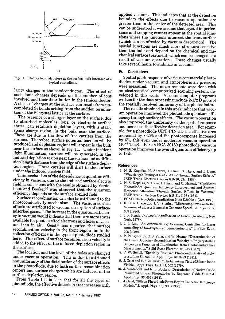
Fig. 11. Energy band structure at the surface bulk interface of atypical photodiode.
larity charges in the semiconductor. The effect ofsuch ionic charges depends on the number of ionsinvolved and their distribution in the semiconductor.A sheet of charges at the surface can result from un-completed Si bonds arising from the sudden termina-tion of the Si crystal lattice at the surface.
The presence of a charged layer on the surface, dueto absorbed molecules, ions, or electronic surfacestates, can establish depletion layers, with a staticspace-charge region, in the bulk near the surface.These are due to the flow of free carriers from thesurface. Therefore, surface potential barriers will beproduced and depletion regions will appear in the bulknear the surface as shown in Fig. 11. Under incidentlight illumination, carriers will be generated in theinduced depletion region near the surface and at diffu-sion length distance from the edge of the surface deple-tion region. These carriers will drift to the surfaceunder the induced electric field.
This mechanism of the dependence of quantum effi-ciency in vacuum, due to the induced surface electricfield, is consistent with the results obtained by Verde-bout and Booker10 who observed that the quantumefficiency depends on the surface applied field.
Surface recombination can also be attributed to thephotoconductivity mechanism. The vacuum surfaceeffects are attributed to vacuum desorption of surface-adsorbed gases. The increase in the quantum efficien-cy in vacuum would indicate that there are more statesavailable for photoexcited electrons and holes in vacu-um than in air. Geist" has reported that surfacerecombination velocity in the front region limits thecollection efficiency in the type of photodiode studiedhere. This effect of surface recombination velocity isadded to the effect of the induced depletion region inthe surface.
The location and the level of the holes are changedunder vacuum operation. This is due to attributednonuniformity of the distribution of the surface effectsin the photodiode, due to both surface recombinationcenters and surface charges which are induced in thesurface depletion region.
From Table I it is seen that for all the types ofphotodiode, the effective detection area increases with
applied vacuum. This indicates that at the detectionboundary the effects due to vacuum operation aregreater than in the center of the detected area. Thiscan be understood if we assume that crystal imperfec-tions and trapping centers appear at the spatial junc-tions where the junctions intersect the front surface(which can be affected by vacuum desorption). Thespatial junctions are much more structure sensitivethan the bulk and depend on the chemical and me-chanical surface treatment, which can be changed as aresult of vacuum operation. These changes usuallytake several hours to stabilize in vacuum.
IV. Conclusions
Spatial photoresponse of various commercial photo-diodes, under vacuum and atmospheric air pressure,were measured. The measurements were done withan electrooptical computerized scanning system, de-veloped in this work. Various computer programswritten for the data processing include 2-1/2 D plots ofthe spatially resolved uniformity of the photodiodes.
The results obtained in this work indicate that vacu-um operation improved the photodiode quantum effi-ciency through surface effects. The vacuum operationalso improved the uniformity of the spatial responseand increased the effective detection area. For exam-ple, for a photodiode UDT-PIN-5D the effective areaincreased by -20% and the photoresponse increasedby 6%, this even under moderate vacuum operation(10-3 Torr). For an RCA 30180 photodiode, vacuumoperation improves the overall quantum efficiency upto 18%.
References
1. N. S. Kopeika, H. Aharoni, I. Hirsh, S. Hava, and I. Lupo,"Wavelength Tuning of GaAs LED's Through Surface Effects,"IEEE Trans. Electron Devices ED-30, 334 (1983).
2. N. S. Kopeika, S. Hava, I. Hirsh, and C. Hazout, "Significant'Photodiodes Quantum Efficiency Improvement and SpectralResponse Alteration Through Surface Effects in Vacuum,"IEEE Trans. Electron Devices ED-31, 1198 (1984).
3. EG&G Electro-Optics Application Note D30000-1 (Oct. 1983).4. K. C. A. Crane and J. V. Sienins, "Microcomputer-Controlled
Scanning of a Laser Beam at a Constant Speed," J. Phys. E. 17,363 (1984).
5. J. F. Ready, Industrial Application of Lasers (Academic, NewYork, 1978).
6. J. J. Lue, "An Automatic x-y Scanning Controller for LaserAnnealing of Ion-Implanted Semiconductors," J. Phys. E. 15,705 (1982).
7. P. Panayotatos, E. S. Yang, and W. Hwang, "Determination ofthe Grain Boundary Recombination Velocity in PolycrystallineSilicon as a Function of Illumination from PhotoconductanceMeasurements," Solid-State Electron. 25, 417 (1982).
8. F. W. Scholl, "Spatially Resolved Photoconductivity of Poly-crystalline Silicon," J. Appl. Phys. 52, 3439 (1981).
9. J. Geist and E. F. Zalewski, "The Quantum Yield of Silicon in theVisible," Appl. Phys. Lett. 35, 502 (1979).
10. J. Verdebout and R. L. Booker, "Degradation of Native OxidePassivated Silicon Photodiodes by Repeated Oxide Bias," J.Appl. Phys. 55, 406 (1984).
11. J. Geist, "Silicon Photodiode Front Region Collection EfficiencyModels," J. Appl. Phys. 51, 3993 (1980).