Compound Semiconductor may 2007 Volume 13 number 4 C ONNECTING THE C OMPOUND S EMICONDUCTOR C OMMUNITY CONVERGENCE HEADLINE NEWS MARKET REPORT Compound logic and the future of digital ICs p16 Looking east Anadigics is to build first chinese GaAs wafer fab for rFics. p5 Tuned up tunable lasers are set to star as the boom times return for fiber-optic components. p12 INFRARED IMAGING Why HgCdTe will aid climate models
Transcript
CompoundSemiconductor
may 2007 Volume 13 number 4
C o n n e C t i n g t h e C o m p o u n d S e m i C o n d u C t o r C o m m u n i t y
CONVERGENCE HEADLINE NEWS MARKET REPORT
Compound logic and the future of digital ICs p16
Looking eastAnadigics is to build first chinese GaAs wafer fab for rFics. p5
Tuned uptunable lasers are set to star as the boom times return for fiber-optic components. p12
INFRARED IMAGING
Why HgCdTe will aid climate models
CSMayCover.indd 1 18/4/07 09:47:58
systems
Oerlikon Innovation:A Vision for the FutureYour partner of choice for high-quality wafer processing equipment.
Liechtenstein T +423 388 4770USA T +1 727 577 49 99China T +86 21 5057 4646Taiwan T +886 3 500 16 88South Korea T +82 31 785 1300Singapore T +65 6873 1188Japan T +81 3 3225 90 20Germany T +49 89 75 505 100www.oerlikon.com
The new brand Oerlikon stands for a long tradition of innovation finding its roots inSwiss precision and service excellence.
Oerlikon Wafer Processing has a leading market position in: Advanced Packaging,Thin Wafer and Multi-Level Metallization, Photomask Etching and CompoundSemi, MEMS and Nanotechnology. Oerlikon providing sales & service as well ascustomer support and training in 40 countries world wide.
Oerlikon Balzers Coating / Wafer ProcessingBooth #119CS MANTECH / May 14 – 17 Austin, Texas, USA
Oerlikon_WP_Compound_May07 11/4/07 10:32 am Page 1
Compound Semiconductor May 2007 compoundsemiconductor.net
Compound Semiconductor’s circulation figures are audited by BPA International
C o n n e C t i n g t h e C o m p o u n d S e m i C o n d u C t o r C o m m u n i t y
induStry
Headline News Anadigics blazes a trail with Chinese fab.
The Month in RFICs High-frequency GaN breakthrough for HRL.
The Month in HBLEDs Lumileds rolls out the Rebels…Nichia seeks injunction…Orders stack up as Aixtron pushes financial performance.
The Month in Optoelectronics CyOptics buys Apogee Photonics…Eblana plots rapid growth with FTTH build-out…Pump-laser makers up the power…Tekcore gets set for GaN laser ramp.
Market Report Tunables in fiber-optic ‘mini-boom’: CIR’s latest analysis of the future market for optical components predicts that sales of tunable lasers will grow rapidly to reach almost $1 billion by 2012. Michael Hatcher reports.
Application Focus PA proves crucial in WiMAX designs: Under pressure to get WiMAX products to market, it may be tempting to overlook the power amplifier, but designers who do so risk degrading system links and reducing battery life, say Glenn Eswein and Ray Waugh from Anadigics.
5
7
8
0
2
4
teChnology
High-k gate stacks point towards digital convergence: Despite the recent application of high-k dielectrics and metal gates in volume CMOS processes, and the scattergun approach to logic devices based on III–V materials, the compound and silicon industries have much in common. Bob Metzger looks at post-CMOS convergence.
Sofradir builds a new factory to ramp HgCdTe chip production: For decades, infrared detector development has drawn on many different types of compound semiconductor material. Philippe Tribolet explains why Sofradir has selected HgCdTe for its future plans. These include building a new $12 million fab to cut chip manufacturing costs, which should ultimately lower detector prices and drive up sales of these high-specification imagers.
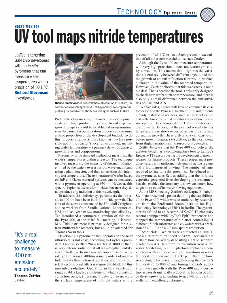
Equipment Update UV tool maps nitride temperatures: LayTec is targeting GaN chip developers with an in situ pyrometer that can measure wafer temperatures with a precision of ±0.1 °C. Richard Stevenson investigates.
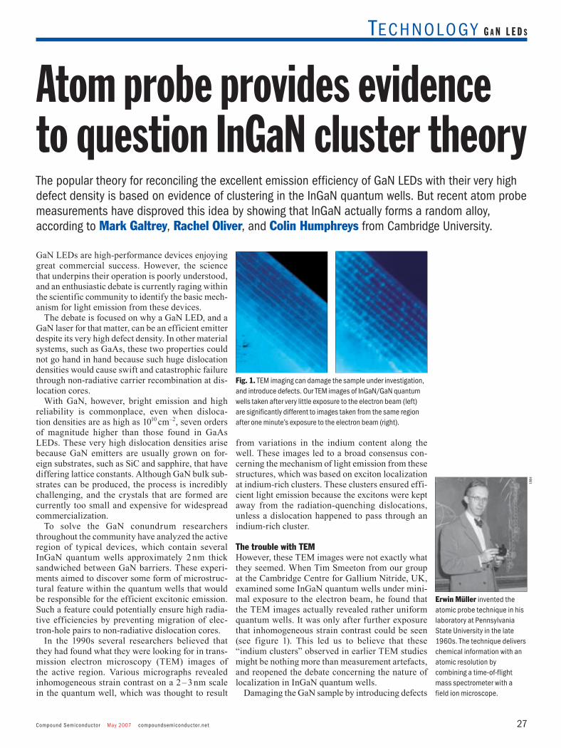
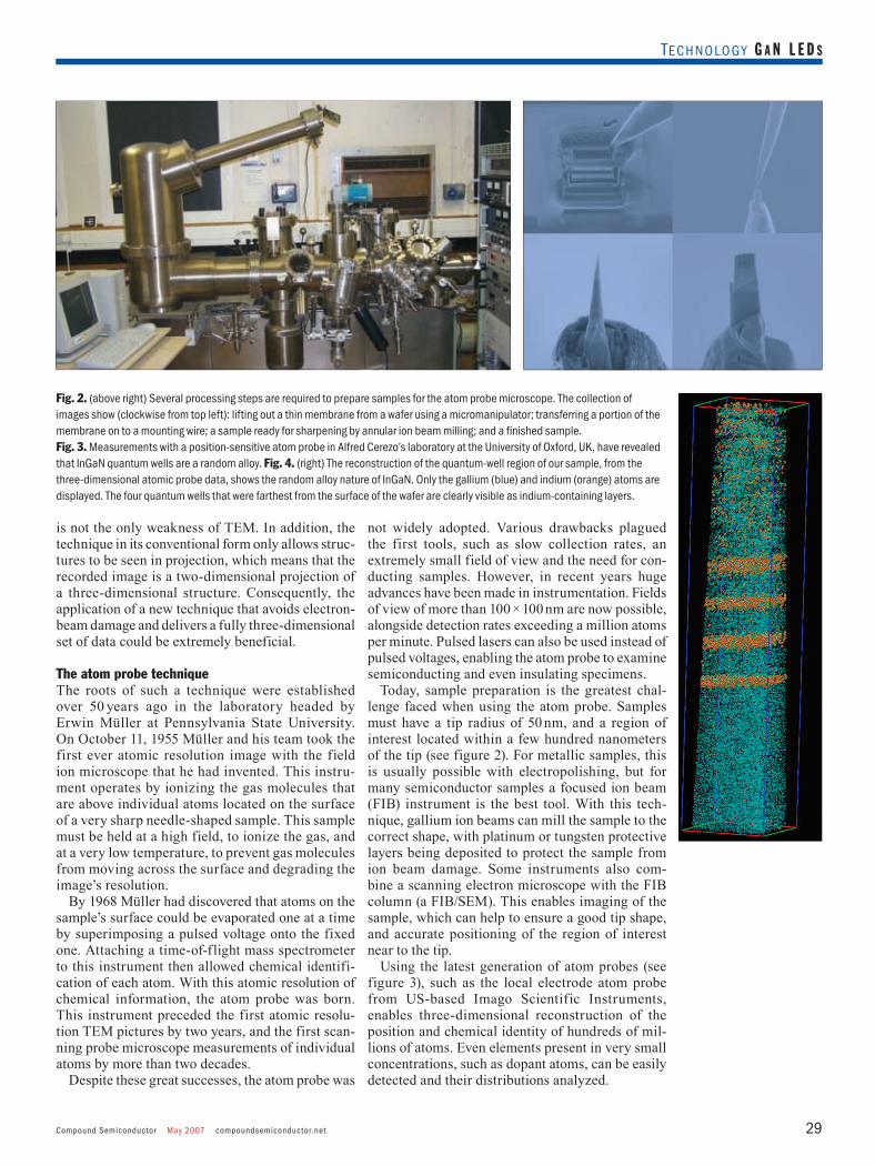
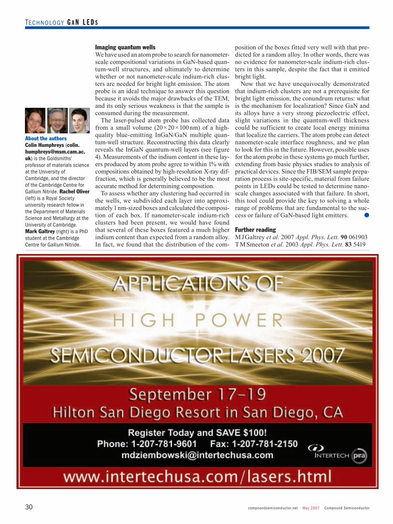
Atom probe provides evidence to question InGaN cluster theory: The popular theory for reconciling the excellent emission efficiency of GaN LEDs with their very high defect density is based on evidence of clustering in the InGaN quantum wells. But recent atom probe measurements have shown that InGaN actually forms a random alloy, according to Mark Galtrey, Rachel Oliver, and Colin Humphreys from Cambridge University.
Product Showcase
Research Review: Researchers build the first ZnO laser…Two phosphors make chips whiter than white.
6
2
25
27
332
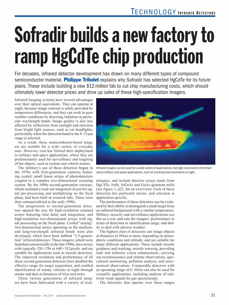
Main cover image: An infrared image (6.7 µm) of the Earth taken in 1994, showing water vapor in the atmosphere in the form of clouds and storms. HgCdTe detectors, which are used regularly for such applications, are discussed in a feature written by Sofradir. See p21. Credit: NASA Goddard/University of Hawaii.
M a y 2 0 07V o l u M e 1 3N u M b e r 4
FabulousAnadigics becomes the first GaAs RFIC maker to take the plunge into China. p5
AnAd
IGIC
S
Probing questionErwin Müller’s 960s technique for analyzing materials has shown how InGan forms a random alloy. p27
HMI
Tuning inSales of tunable lasers are growing fast, but this time around there will be no “bust”. p12
Production Anny MortadaAd production Mark TrimnellArt director Andrew GiaquintoTechnical illustrator Alison Tovey
SubscriptionsAvailable free of charge to qualifying individuals working at compound semiconductor fabs and foundries. For further information visit compoundsemiconductor.net/subscribe. Subscriptions for individuals not meeting qualifying criteria: individual £90/$165 US/€135; library £199/$360 US/€290. Orders to: Compound Semiconductor, WDIS, Units 12 & 13, Cranleigh Gardens Industrial Estate, Southall, Middlesex UB1 2DB, UK. Tel +44 208 606 7518; Fax +44 208 606 7303. General enquiries: [email protected].
9025 average total qualified circulation**December 2006 BPA audit statement
Editorial boardMayank Bulsara Atlas Technology (USA); Andrew Carter Bookham Technology (UK); Jacob Tarn OCP/Gigacomm (Taiwan); Ian Ferguson Georgia Institute of Technology (USA); Toby Strite JDSU (USA); Mark Wilson Motorola (USA); Dwight Streit Northrop Grumman (USA); Joseph Smart Crystal IS (USA); Colombo Bolognesi Swiss Federal Institute of Technology (Switzerland); Shuji Nakamura University of California at Santa Barbara (USA)
US mailing information: Compound Semiconductor (ISSN 1096-598X) is published 11 times a year for $165 by IOP Publishing, Dirac House, Temple Back, Bristol BS1 6BE, UK. Periodicals postage paid at Middlesex, NJ 08846. POSTMASTER: send address corrections to Compound Semiconductor, c/o PO Box 177, Middlesex, NJ 08846. US agent: Pronto Mailers Association Inc, 200 Wood Avenue, PO Box 177, Middlesex, NJ 08846.
Among a whole barrage of wafer capacity upgrades announced within the past month, one stands out – Anadigics’ decision to construct a new 6 inch fab from scratch in China marks an important milestone for the compound semiconductor business.
The New Jersey company likes to think of itself as one of the early innovators in the III–V industry, and rightly so. Over the years it has led the way with 6 inch wafer fabrication of RFICs, the development of integrated BiFET chip structures, and power amplifiers for next-generation broadband technologies like WiMAX.
Spend a few minutes talking to Anadigics CEO Bami Bastani, and it is easy to see how the company has found itself taking this course. “Innovation, innovation, innovation” is Bastani’s mantra; the talk of a man who knows that his engineering team is his prized asset. But the road has not been easy for Anadigics.
Rather than chase after the GSM business, Bastani and his team decided to take a calculated risk on the broadband wireless technology of the future. Well, it must have seemed like a long time coming, and Anadigics has endured some tough times. But now that broadband ship is
coming in – and Anadigics is set to reap the benefits.Bastani is understandably thrilled about the new Chinese GaAs wafer
fab, and so are the local dignitaries in Kunshan, who see this as a flagship development for their high-tech industrial zone. Anadigics will be the first semiconductor chip maker in the local area, but Bastani acknowledges that the inroads made by silicon companies, such as Intel, in other parts of China have been crucial in paving the way for compounds.
The new Anadigics fab will combine experience from the worlds of both silicon and compound chip manufacturing. And this is something that is also going to be crucial for the future of digital ICs. Convergence is the key word here, and, as we report on page 16 of this issue, it means this: the compound and silicon semiconductor industries need to get their heads together to ensure that digital ICs continue to scale beyond what is possible with conventional CMOS processes. It will demand innovators like Bastani in both camps to make this happen.
Your premier choice for III-V and Ge substrates andrelated strategic raw materials.AXT is committed to our valued customers, ensuring superior technology, products and customer service.
Please visit axt.com to see why we are the premier source for VGF technology.
Germanium S U B S T R AT E S
Enabling the production of solar cells for
space and terrestrial applications
USA Headquarters4281 Technology DriveFremont, CA, USA 94538Tel: 510-438-4700Fax: 510-353-0668Email: [email protected]
ChinaBeijing Tongmei Xtal Technology4 Eastern Second StreetIndustrial Development ZoneTongzhou District, Beijing, China 101113Tel: 86-10-6156-2241Fax: 86-10-6156-2245Email: [email protected]
Japan EastMBK Microtek, Inc.Shuwa Shiba Park Bldg A-10F4-1 Shibakoen 2-chomeMinato-ku, Tokyo, Japan 105-0011 Tel: 81-3-5733-0701Fax: 81-3-5733-0702Email: [email protected]
Japan WestMo Sangyo Co, LTD.201 Ashiya-Farfalla, 6-16 Narihira-choAshiya-Hyogo, Japan 659-0068Tel: 81-797-32-0046Fax: 81-797-32-0304Email: [email protected]
TaiwanConary Enterprise Co., Ltd.10F No. 28, Sec. 3, Nan-King East RoadTaipei, Taiwan, R.O.C.Tel: 886-2-2509-1399Fax: 886-2-2501-6279Email: [email protected]
Compound Semiconductor May 2007 compoundsemiconductor.net
Indus tr y H e a d l i n e n e w s
G a A s C H I P M A N U FA C T U R I N G
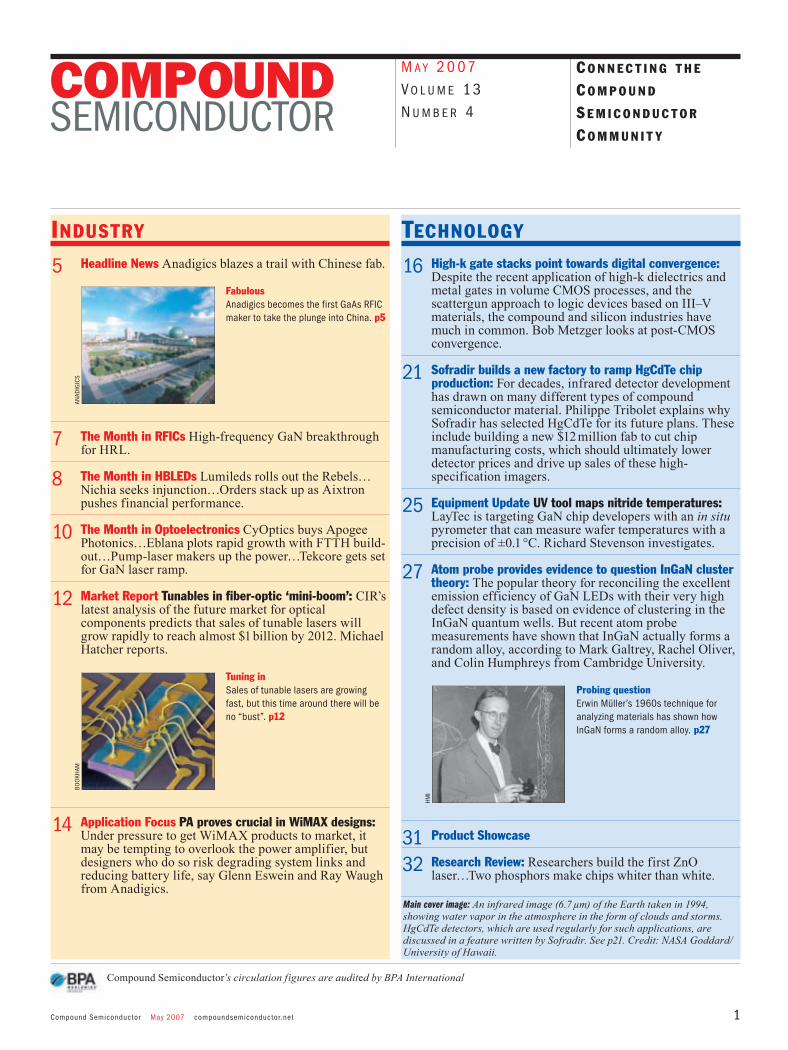
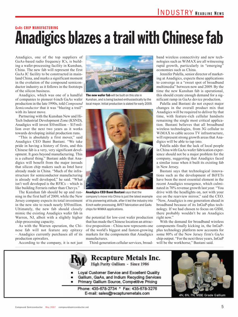
Anadigics, one of the top suppliers of GaAs-based radio frequency ICs, is build-ing a wafer-processing facility in Kunshan, China. The new fab will represent the first GaAs IC facility to be constructed in main-land China, and marks a significant moment in the evolution of the compound semicon-ductor industry as it follows in the footsteps of the silicon business.
Anadigics, which was one of a handful of companies to pioneer 6 inch GaAs wafer production in the late 1990s, told Compound Semiconductor that it was “blazing a trail” with its latest move.
Partnering with the Kunshan New and Hi-Tech Industrial Development Zone (KSND), Anadigics will invest $10 million – $15 mil-lion over the next two years as it works towards developing initial production runs.
“This is absolutely a first mover,” said Anadigics CEO Bami Bastani. “We take pride in having a history of firsts, and this Chinese fab is a very, very significant devel-opment. It goes beyond manufacturing. This is a cultural thing.” Bastani adds that Ana-digics will benefit from the major inroads that silicon chip makers such as Intel have already made in China. “Much of the infra-structure for semiconductor manufacturing is already well developed,” he said. “What isn’t well developed is the RFICs – which is like building Ferraris rather than Chevys.”
The Kunshan fab should be up and run-ning in the first half of 2009, while the New Jersey company expects its total investment in the new site to reach nearly $50 million. Ultimately, the new fab should closely mimic the existing Anadigics wafer fab in Warren, NJ, albeit with a slightly higher chip-processing capacity.
As with the Warren operation, the Chi-nese fab will not feature any epitaxy – Anadigics currently purchases all of its production epiwafers.
According to the company, it is not just
the potential for low-cost wafer production that has made the Chinese location an attrac-tive proposition – China now represents one of the world’s biggest and fastest-growing markets for the components that Anadigics manufactures.
Third-generation cellular services, broad-
band wireless connectivity and new tech-nologies such as WiMAX are all witnessing rapid growth, particularly in “emerging” economies such as China.
Jennifer Palella, senior director of market-ing at Anadigics, expects these applications to converge in a “sweet spot of broadband multimedia” between now and 2009. By the time the new Kunshan fab is operational, this should create enough demand for a sig-nificant ramp in GaAs device production.
Palella and Bastani do not expect major changes in the overall product mix that Anadigics will be required to deliver by that time, with feature-rich cellular handsets remaining the single most critical applica-tion. Bastani believes that all broadband wireless technologies, from 3G cellular to WiMAX to cable access TV infrastructure, will represent strong growth areas that Ana-digics will be able to tap into.
Palella adds that the lack of local people in China with GaAs wafer fabrication exper-ience should not be a major problem for the company, suggesting that Anadigics faced a similar issue when it built its existing fab in New Jersey.
Bastani says that technological innova-tions such as the development of BiFETs have been the most essential element in the recent Anadigics resurgence, which culmi-nated in 70% revenue growth last year. “You drive with the headlights on, not with your eye on the rearview mirror,” said the CEO. “Now, Anadigics is one generation ahead in broadband because of its InGaP-plus tech-nology. If we had chosen to focus on GSM, there probably wouldn’t be an Anadigics right now.”
With the demand for broadband wireless components finally kicking in, the InGaP-plus technology platform now accounts for some 80% of the New Jersey firm’s GaAs chip output. “For the next three years, InGaP will be the workhorse,” Bastani said.
Anadigics blazes a trail with Chinese fab
The new wafer fab will be built on this site in Kunshan, and is being backed enthusiastically by the local mayor. Initial production is slated for early 2009.
Anadigics CEO Bami Bastani says that the company’s move into China is just the latest example of its pioneering attitude, after it led the industry into 6 inch wafer processing, BiFET fabrication and GaAs chips for WiMAX applications.
AMERICAN SCIENTIFIC PUBLISHERS 25650 North Lewis Way, Stevenson Ranch, California 91381-1439, USAFax: (661) 254-1207 Phone: (661) 254-0807 Email: [email protected]
Order online at: www.aspbs.comOrder online at: www.aspbs.comOR
DE
R
FR
OM
A M E R I C A NSCIENTIFICPUBLISHERS
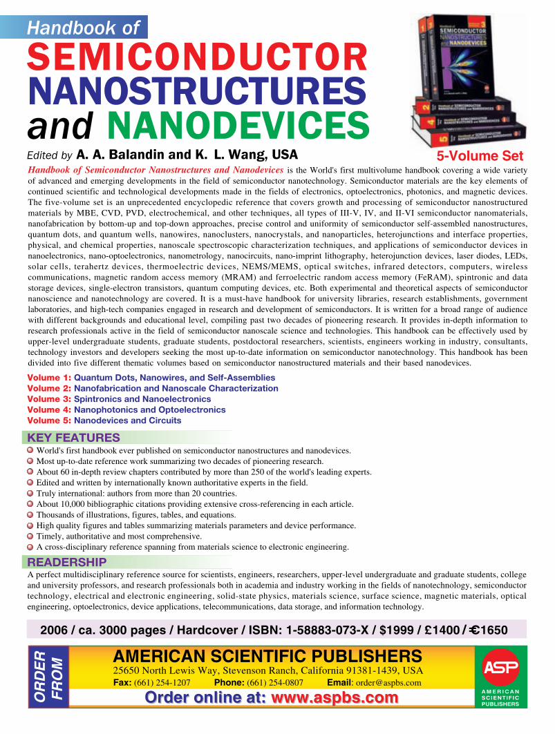
Handbook of Semiconductor Nanostructures and Nanodevices is the World's first multivolume handbook covering a wide variety of advanced and emerging developments in the field of semiconductor nanotechnology. Semiconductor materials are the key elements of continued scientific and technological developments made in the fields of electronics, optoelectronics, photonics, and magnetic devices. The five-volume set is an unprecedented encyclopedic reference that covers growth and processing of semiconductor nanostructured materials by MBE, CVD, PVD, electrochemical, and other techniques, all types of III-V, IV, and II-VI semiconductor nanomaterials, nanofabrication by bottom-up and top-down approaches, precise control and uniformity of semiconductor self-assembled nanostructures, quantum dots, and quantum wells, nanowires, nanoclusters, nanocrystals, and nanoparticles, heterojunctions and interface properties, physical, and chemical properties, nanoscale spectroscopic characterization techniques, and applications of semiconductor devices in nanoelectronics, nano-optoelectronics, nanometrology, nanocircuits, nano-imprint lithography, heterojunction devices, laser diodes, LEDs, solar cells, terahertz devices, thermoelectric devices, NEMS/MEMS, optical switches, infrared detectors, computers, wireless communications, magnetic random access memory (MRAM) and ferroelectric random access memory (FeRAM), spintronic and data storage devices, single-electron transistors, quantum computing devices, etc. Both experimental and theoretical aspects of semiconductor nanoscience and nanotechnology are covered. It is a must-have handbook for university libraries, research establishments, government laboratories, and high-tech companies engaged in research and development of semiconductors. It is written for a broad range of audience with different backgrounds and educational level, compiling past two decades of pioneering research. It provides in-depth information to research professionals active in the field of semiconductor nanoscale science and technologies. This handbook can be effectively used by upper-level undergraduate students, graduate students, postdoctoral researchers, scientists, engineers working in industry, consultants, technology investors and developers seeking the most up-to-date information on semiconductor nanotechnology. This handbook has been divided into five different thematic volumes based on semiconductor nanostructured materials and their based nanodevices.
World's first handbook ever published on semiconductor nanostructures and nanodevices. Most up-to-date reference work summarizing two decades of pioneering research. About 60 in-depth review chapters contributed by more than 250 of the world's leading experts. Edited and written by internationally known authoritative experts in the field. Truly international: authors from more than 20 countries. About 10,000 bibliographic citations providing extensive cross-referencing in each article. Thousands of illustrations, figures, tables, and equations. High quality figures and tables summarizing materials parameters and device performance. Timely, authoritative and most comprehensive. A cross-disciplinary reference spanning from materials science to electronic engineering.
Volume 1: Quantum Dots, Nanowires, and Self-AssembliesVolume 2: Nanofabrication and Nanoscale Characterization Volume 3: Spintronics and NanoelectronicsVolume 4: Nanophotonics and OptoelectronicsVolume 5: Nanodevices and Circuits
SEMICONDUCTORNANOSTRUCTURESand NANODEVICES
5-Volume SetEdited by A. A. Balandin and K. L. Wang, USA
Handbook of
A perfect multidisciplinary reference source for scientists, engineers, researchers, upper-level undergraduate and graduate students, college and university professors, and research professionals both in academia and industry working in the fields of nanotechnology, semiconductor technology, electrical and electronic engineering, solid-state physics, materials science, surface science, magnetic materials, optical engineering, optoelectronics, device applications, telecommunications, data storage, and information technology.
Compound Semiconductor May 2007 compoundsemiconductor.net 7
Indus t r y T h e M o n T h i n R F i C s
By Andy ExtanceThe development and deployment of broad bandwidth wireless links has received a significant boost, with research laboratory HRL unveiling a new GaN-based power amplifier for high-frequency applications.
“Our product development roadmap calls for a roll-out in late 2007,” HRL told Com-pound Semiconductor. “In the near term (2008–2009), [HRL] foresees market sizes as large as 10,000–100,000 chips/year.”
As well as being the first GaN MMIC amplifier to target the specific “W-band” frequency range (75–10 GHz), the compo-nent boasts a power density of 2.1 W/mm, as compared to just 0.26 W/mm in the equiva-lent InP chip that HRL previously consid-ered to be state of the art.
These high-performance chips were made using plasma-assisted MBE to grow heavily doped GaN and AlGaN cap layers, and to deposit low-resistance ohmic contacts. Also key to making the chip was an AlGaN/GaN/AlGaN double heterojunction that reduced short-junction effects, and development of means to dry-etch slot vias.
“Until very recently GaN-based devices were not seriously considered for power applications at frequencies that are higher
than 50 GHz, due to difficulty with material processing and the lack of a device structure suitable for high-frequency applications,” explained HRL.
The output frequencies encompassed by the new device include the three E-band spectrum segments approved in the US for gigabit-rate wireless links, and this innova-tion could translate to a threefold increase in operating range for HRL’s broadband communication protocol.
HRL suggests that the level of amplifica-tion achieved in the MMIC will allow the development of cost-effective wireless data transmission at 10 Gb/s, and increase the operating range of radar systems by 70%.
Due to the smaller chip size per watt emit-ted, these chips also offer higher efficiency at high power levels, leading to reduced cooling requirements and lower costs.
The improvements that the GaN MMICs could bring to millimeter-wave broadband wireless communications strengthen the case for this being the preferred technol-ogy for high-speed data transfer, beyond the avoidance of logistical issues associated with installing fiber-optic infrastructure.
Gigabeam, the US gigabit wireless com-munication specialist, has agreed a contract with the Ministry of the Interior of the King-dom of Bahrain for a high-speed network linking government buildings across the country. Gigabeam will receive $1.37 mil-lion to work with Motorola and Cisco in the provision of the backbone infrastructure.
W I D E- B A N D G A P T R A N S I S T O R S
High-frequency GaN breakthrough for HRL
...Raining PAs at CTIAThe CTIA Wireless trade show in Orlando witnessed the launch of a variety of new RFIC products from GaAs chip manufacturers. Anadigics says that its revolutionary “ZeroIC” power amplifier (PA) for CDMA cell phones yields a dramatic decrease in power consumption. Power consumption is claimed to decrease to zero when a handset only needs to transmit at a very low power, for example, in a fully populated network.
Other products debuting at CTIA included a new front-end module for mobile WiMAX from Skyworks Solutions and two new PA modules from RF Micro Devices.
...Motorola bombshellA dismal trading update from Motorola could spell trouble for GaAs chip manufacturers RF Micro Devices and Skyworks Solutions. “Performance in our mobile devices business continues to be unacceptable,” said CEO Ed
Zander. “We now recognize that returning the business to acceptable performance will take more time and greater effort.” Motorola’s handset woes are twofold: it has a limited portfolio for the high-end 3G sector; and in emerging markets such as Africa, India and South Asia, it appears to be unable to compete on price with its main rivals.
As major suppliers to the top-ranking phone vendors, Skyworks and RFMD are very exposed to Motorola’s misfortune – although the drop may be offset by sales to other handset makers taking Motorola’s market share.
…Nitronex moves HQGaN-on-silicon transistor specialist Nitronex plans to move its corporate headquarters across North Carolina from Raleigh to Durham’s Research Triangle Park area. The switch enhances the company’s manufacturing capability and allows it to expand its research and development efforts.
From our web pages...visit compoundsemiconductor.net for daily news updates
compoundsemiconductor.net May 2007 Compound Semiconductor
Indus t r y T h e M o n T h i n h B L e D s
Nichia Corporation has filed for a provi-sional injunction against Sterling Inc., a Tokyo-based gift manufacturer, after nego-tiations aimed at resolving the issue outside the courts broke down.
Nichia is intervening over the white LEDs in Sterling’s 4505 LED palm radio light and other products. COTCO, a subsidiary of the US LED manufacturer Cree since its acqui-sition was completed on April 2, is named by Nichia as the source for the white LEDs used in the device.
However, Nichia confirmed that the offending articles bear the slogan “COTCO LED Technology powered by Cree US Pat 6,600,175”. Both Nichia and Cree hold pat-ents on using phosphors with blue LED
chips to manufacture white LEDs.Nichia is seeking to uphold its Japanese
patent, No. 3065263, which uses a blue LED chip with a single-wire structure, and a yel-low phosphor to down-convert the incident frequency to finally give white light.
The US patent that Nichia names, origi-nally filed by ATMI but owned by Cree after a prior acquisition, also contains claims concerning arrays which use phos-phors to down-convert light from a blue LED to white light.
Nichia and Cree have clashed before over this technology, but have since resolved their disputes. The Japanese chip maker signals its intentions by saying that it would continue to “take necessary measures against any companies who infringe Nich-ia’s intellectual property rights in any part of the world.” Cree declined to comment on Nichia’s move.
l e g a l a c t i o n
Philips Lumileds has launched a wide- ranging suite of compact new LED products known as the Luxeon Rebel family.
Based on both InGaN and AlInGaP, the Rebel LEDs feature Lumileds’ latest chip technologies. Available in a wide range of colors – from various whites to royal blue, green, red and amber – the Rebels have been designed with solid-state lighting in mind.
“Luxeon Rebel will cause a rapid change in solid-state lighting design,” predicted David Eastley from the San Jose, CA, chip-manufacturing company.
Crucially, the new products include “warm-white” and so-called “neutral-white” emitters, essentially white sources with a lower color temperature than most previous power LEDs. These “warmer” hues are important as they imitate the color of traditional incandescent lamps and are therefore preferable for interior residential lighting applications.
Lumileds claims that all the chips in the Rebel family are engineered to operate between 350 mA and 1 A, with the cool-white emitter offering the highest efficacy of over 70 lm/W. In its data sheet, however, Lumileds only quotes typical lumen output performance at 350 mA and 700 mA.
At the lower drive current, the cool-white chips emit a minimum of 80 lm, equating to a luminous efficacy of about 73 lm/W. At 750 mA, the luminous flux increases to a “typical” value of 145 lm, with the efficacy dropping to approximately 61 lm/W.
If higher total light output is desired, the cool-white chip is said to deliver more than
160 lm at a high drive current. The warm-white Rebels are rated at a lower luminous flux, delivering a minimum of 60 lm at 350 mA and typically 110 lm at 700 mA.
Lumileds has already stockpiled plenty of the Rebels with its distribution partner Future Lighting Solutions, although the warm-white and neutral-white LEDs have only just become available for sampling. Vol-ume production of these two important chips is slated to begin later this year.
The new chips from Lumileds will be up against stiff competition in the solid-state lighting sector from traditional rivals like Cree and Nichia. Cree already has XLamp products with a similar performance to the Rebel in volume production, while Nichia is expected to launch a lighting-class power LED later this year.
Cree says that its XR-E chips, which are being used in solar-powered streetlights in China, also deliver a typical flux of 80 lm of cool-white light when driven at 350 mA, and 65 lm of warm-white at the same current.
Cree also quotes a typical luminous flux of 136 lm at the higher drive current of 700 mA for the cool-white XR-E chips, dropping to 100 lm for warm-white emission.
The XR-E is also said to have a typical flux of 176 lm at a 1 A drive current, although no figure is given for warm-white at this level.
Perhaps pre-empting the Rebel release, Cree recently released its new XLamp products, which it says represent the first “lighting-class” warm-white LED sources. They are able to deliver up to 124 lm when driven at 700 mA.
Compound Semiconductor May 2007 compoundsemiconductor.net
Indus t r y T h e M o n T h i n h B L e D s
M O C V D E Q U I P M E N T S A L E S
Germany-based epitaxy equipment vendor Aixtron returned to profit in 2006 on the back of strong performances in both its com-pound semiconductor and silicon divisions.
The company, which has enjoyed strong sales for its newest range of MOCVD equip-ment, posted a net profit of €5.9 million ($7.8 million) on total sales of €171.7 million in 2006.
A hike in gross margin from 35% to 64% enabled Aixtron to easily exceed its original financial target of breaking even in 2006, an understandably cautious goal that was set after it had made a net loss of €53.7 mil-lion in 2005.
Of the 2006 sales, 56% were attributable to compound semiconductor applications – including both MOCVD equipment and organic deposition tools – reflecting Aix-tron’s strategy to become less dependent on the compounds market, also highlighting the impact of its investment in the advanced
silicon deposition specialist Genus.Revenues from compound semiconduc-
tor applications jumped 20% year-on-year, while a reduction in administrative over-heads also contributed to the much healthier bottom-line performance.
2006 was also a very strong year for order intake at Aixtron. Orders rose by 79% to €136.8 million. This boom was largely due to a sharp rise in demand from makers of high-brightness LEDs throughout 2006.
With a healthy order backlog of €85.1 million, Aixtron CEO Paul Hyland believes that the company will post sales of between €190 million and €200 million in 2007, and improve net profit to around the €15 million mark.
Aixtron aims to maintain a market share of 60%, equivalent to sales of $141 million, through 2009, by when the annual market for all MOCVD equipment is predicted by VLSI Research to reach $235 million.
Orders stack up as Aixtron pushes financial performance ...Samsung goes for quick ramp
Samsung Electro-Mechanics (SEMCO) has ordered two more MOCVD systems from Aixtron to ramp blue and white LED production. The AIX 2600G3HT machines are set to be delivered to SEMCO’s fab in Kyungki-Do, Korea.
...Berlin researchers head into the UVResearchers at the Technical University of Berlin in Germany have ordered a Thomas Swan MOCVD reactor to develop high-performance ultraviolet AlGaN emitters.
“[The new tool] will be a useful platform for us to develop high-aluminum-III-nitride laser diodes and high-brightness ultraviolet LEDs,” said lead researcher Michael Kneissl.
...Cutting GaN wafer costs Management consultants say that BluGlass’ GaN deposition technique could cut LED epiwafer production costs by 48%. The consultants compared 21 × 2 inch epiwafer production using MOCVD with BluGlass’s remote plasma CVD (RPCVD) approach.
From our web pages...visit compoundsemiconductor.net for daily news updates
Extend your knowledge – become a member of
compoundsemiconductor.net today
Join thousands of other professionals from thecompound semiconductor industry who areenjoying the benefits of being a member of
compoundsemiconductor.net.
It’s quick, easy and free to sign up as amember, so join today
compoundsemiconductor.net May 2007 Compound Semiconductor10
Indus t r y T h e M o n T h i n o p T o e l e c T r o n i c s
Eblana Photonics, the Irish developer of high-speed lasers, will benefit from the expected build-out of fiber-to-the-home (FTTH) com-munications in the US this year.
With the service provider Verizon plan-ning to deploy a million of these high-speed links direct to homes during 2007, Eblana CEO James O’Gorman says that the Dub-lin company’s long-held vision of an out-sourced volume manufacturing model has been vindicated. Eblana’s chips are made on a 4 inch platform at the InP foundry owned by the US company Vitesse.
At the optical-fiber communication con-ference in March, Eblana launched new products for both FTTH and 10 Gigabit Eth-ernet applications, two of the fastest-growing sectors in the optical networking business.
The new lasers include single-mode emit-ters that are similar to Fabry–Pérot designs and work over an extended temperature range of –40 C to 85 C, making them suitable for outdoor deployment in FTTH networks.
O’Gorman says that the low-cost chips are much simpler to fabricate than distrib-uted feedback (DFB) lasers because they do not involve an awkward regrowth step. This
is one reason why transceivers featuring the chips can be manufactured at a much lower overall production cost.
In addition, the Eblana lasers do not require any optical isolator components, meaning that transceivers based around them have much higher manufacturing yields than those featuring DFB lasers. This is because DFB lasers can exhibit mode-hopping under certain operating con-ditions, and transceivers sometimes have to be rebuilt as a result. The unacceptable yields translate into much more expensive transceivers, says O’Gorman.
F I B E R - O P T I C C O M P O N E N T S
InP optoelectronic component foundry CyOptics is set to acquire chip manufacturer and close neighbor Apogee Photonics.
The deal is a clear sign of renewed con-solidation in the optoelectronics business, which recently saw Avanex hand ownership of its InP and GaAs fab to a serial entrepre-neur, and JDSU acquire Picolight.
Allentown-based Apogee is a key supplier of high-performance, uncooled laser chips for 10 Gb/s and 40 Gb/s optical communica-tion networks, and the acquisition further bolsters CyOptics’ position as a single source for a wide range of such components.
CyOptics says that it will switch Apogee’s chip fab operations in Allentown to within its own InP facility, which is only eight miles away in Lehigh Valley. The Allen-town fab covers all processes from epitaxy through to wafer dicing.
“The industry is continuing its consolida-tion and CyOptics is growing its revenue by offering our customers one-stop shopping for best-in-class component solutions,” said CyOptics CEO Ed Coringrato.Apogee was formed in July 2005 through
the merger of T-Networks and ASIP, just two months after CyOptics had emerged as a key player in the consolidation of the optical components industry with the acquisition of TriQuint’s optoelectronics business unit.
The value of the latest deal has not been disclosed, but it seems unlikely that the ven-ture capitalists who invested a total of nearly $70 million in Apogee over the last few years will have recouped all of that cash.
However, the future for CyOptics looks bright. Apogee CEO Mike Decelle says that the combination of CyOptics and Apogee would benefit from a complementary line-up of products and customers. “Apogee has established a leadership position in high-speed lasers, so CyOptics is well positioned to address all of the high-growth markets for optical components,” Decelle said.
Products set for rapid growth in demand include 10 Gb/s and 40 Gb/s lasers and detec-tors for pluggable transceivers, tunable laser transmitters, optical components for broad-band access networks such as fiber-to-the-home, and photonic integrated circuits for next-generation network applications.
M E R G E R S & A C Q U I S I T I O N S
Eblana plots rapid growth with FTTH build-out
CyOptics buys Apogee Photonics
All hooked up: Verizon is pioneering FTTH in the US
Compound Semiconductor May 2007 compoundsemiconductor.net 11
Indus t r y T h e M o n T h i n o p T o e l e c T r o n i c s
Epitaxy equipment vendor Aixtron has received a purchase order from the Taiwan-ese company Tekcore for a production sys-tem designed to manufacture blue–violet lasers based on GaN.
The AIX 2400G3 HT “integrated con-cept” MOCVD reactor, which supports 11 × 2 inch wafer production, will be installed at Tekcore’s semiconductor fab at Nantou in Taiwan.
Blue–violet laser producers are now gear-ing up for a widespread ramp to high vol-umes, in anticipation of increasing demand for their use in high-definition DVD players and recorders. Sony has already had to pro-duce millions of blue lasers to support the roll-out of its PlayStation3 games console, while Sharp recently revealed plans to ramp up production of high-power GaN lasers for use in high-definition DVD equipment.
In addition, Nichia says that it has devel-oped a 320 mW pulsed diode laser, which it is expected to commercialize in 2008.
F I B E R - O P T I C C O M P O N E N T S
Laser chip manufacturers JDSU, Bookham and Lumics all showed off new high-power designs at the recent optical-fiber com-munication conference and exhibition in Anaheim, CA. The companies are targeting the erbium-doped fiber amplifier (EDFA) market with new 980 nm lasers that can cut costs, reduce power consumption and improve amplifier reliability.
California-based JDSU has released two new products, including a 660 mW source. The high output power of the 3000 series helps to cut amplifier costs because fewer lasers are needed to pump the amplifier, while overall noise is also reduced.
JDSU has also released a 400 mW laser for similar applications. While this pump does use a cooler, it only regulates the chip temperature to 45 C instead of the usual 25 C. Toby Strite from the company explains that this means less cooling horse-power is needed in a worst-case scenario, saving 20% or more on the total power dis-sipation and consumption budgets.
“Coolerless pumps, in our view, are niche products, used, for example, undersea,” Strite explained. “The few dollars one saves eliminating the cooler are more than offset
by the other design changes required to accommodate a chip temperature which can swing from zero to 75 C in a normal tele-com system while still having to be locked to a single emission wavelength by a fiber Bragg grating.”
JDSU’s Bay Area neighbor Bookham is also releasing a new 980 nm source. The firm manufactures these lasers at its GaAs semiconductor fab in Zurich, Switzerland, which JDSU actually used to own until its 2001 merger with SDL. Bookham says that its new LC96 pumps offer a “kink-free” output power of 750 mW.
Meanwhile, Lumics, which runs a high-power-laser chip fab at its headquarters in Berlin, Germany, has also improved the performance of its 980 nm product line. Lumics says that its compact “Mini-DIL” source operates kink-free at up to 220 mW without any need for cooling. The lasers are Telcordia-qualified for up to 200 mW oper-ating power.
The firm says that its proprietary chip technology allows the uncooled operation, and that EDFA makers will benefit from a significant reduction in the size and power consumption of their products.
B L U E – v I O L E T E M I T T E R S
Pump-laser makers up the power
Tekcore gets set for GaN laser ramp
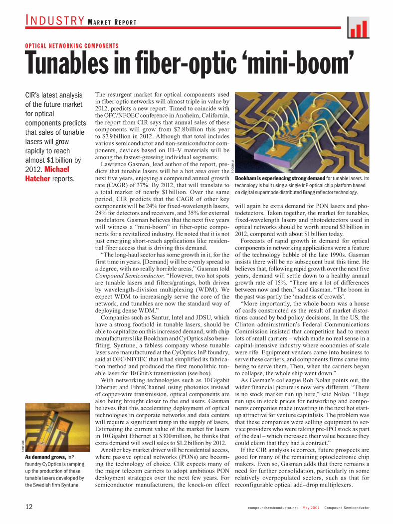
Scientists from IBM have developed a prototype optical transceiver chipset capable of speeds of 160 Gbit/s. The transceiver, which, in theory, could download a feature-length film in 1 s, is largely based on a CMOS chipset that performs driver and receiver functions. But the transmitter function still relies on III–V technology, and a 4 × 4 VCSEL array is integrated within the transceiver.
IBM claims that the tiny optical chipset, which measures just 3.25 × 5.25 mm, is the world’s fastest. However, rivals such as Infinera have made larger integrated chipsets that have been clocked at 1.6 Tb/s, based on individual 40 Gb/s components.
compoundsemiconductor.net May 2007 Compound Semiconductor12
Indus tr y M a r k e t r e p o r t
The resurgent market for optical components used in fiber-optic networks will almost triple in value by 2012, predicts a new report. Timed to coincide with the OFC/NFOEC conference in Anaheim, California, the report from CIR says that annual sales of these components will grow from $2.8 billion this year to $7.9 billion in 2012. Although that total includes various semiconductor and non-semiconductor com-ponents, devices based on III–V materials will be among the fastest-growing individual segments.
Lawrence Gasman, lead author of the report, pre-dicts that tunable lasers will be a hot area over the next five years, enjoying a compound annual growth rate (CAGR) of 37%. By 2012, that will translate to a total market of nearly $1 billion. Over the same period, CIR predicts that the CAGR of other key components will be 24% for fixed-wavelength lasers, 28% for detectors and receivers, and 35% for external modulators. Gasman believes that the next five years will witness a “mini-boom” in fiber-optic compo-nents for a revitalized industry. He noted that it is not just emerging short-reach applications like residen-tial fiber access that is driving this demand.
“The long-haul sector has some growth in it, for the first time in years. [Demand] will be evenly spread to a degree, with no really horrible areas,” Gasman told Compound Semiconductor. “However, two hot spots are tunable lasers and filters/gratings, both driven by wavelength-division multiplexing (WDM). We expect WDM to increasingly serve the core of the network, and tunables are now the standard way of deploying dense WDM.”
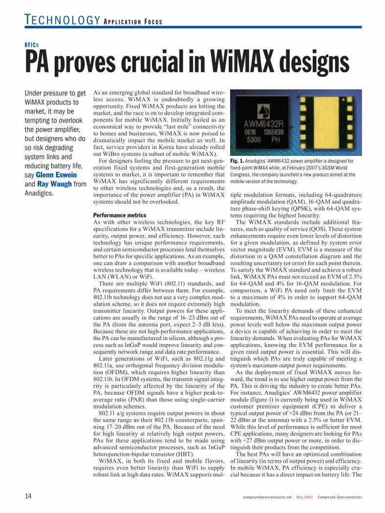
Companies such as Santur, Intel and JDSU, which have a strong foothold in tunable lasers, should be able to capitalize on this increased demand, with chip manufacturers like Bookham and CyOptics also bene-fiting. Syntune, a fabless company whose tunable lasers are manufactured at the CyOptics InP foundry, said at OFC/NFOEC that it had simplified its fabrica-tion method and produced the first monolithic tun-able laser for 10 Gbit/s transmission (see box).
With networking technologies such as 10 Gigabit Ethernet and FibreChannel using photonics instead of copper-wire transmission, optical components are also being brought closer to the end users. Gasman believes that this accelerating deployment of optical technologies in corporate networks and data centers will require a significant ramp in the supply of lasers. Estimating the current value of the market for lasers in 10 Gigabit Ethernet at $300 million, he thinks that extra demand will swell sales to $1.2 billion by 2012.
Another key market driver will be residential access, where passive optical networks (PONs) are becom-ing the technology of choice. CIR expects many of the major telecom carriers to adopt ambitious PON deployment strategies over the next few years. For semiconductor manufacturers, the knock-on effect
will again be extra demand for PON lasers and pho-todetectors. Taken together, the market for tunables, fixed-wavelength lasers and photodetectors used in optical networks should be worth around $3 billion in 2012, compared with about $1 billion today.
Forecasts of rapid growth in demand for optical components in networking applications were a feature of the technology bubble of the late 1990s. Gasman insists there will be no subsequent bust this time. He believes that, following rapid growth over the next five years, demand will settle down to a healthy annual growth rate of 15%. “There are a lot of differences between now and then,” said Gasman. “The boom in the past was partly the ‘madness of crowds’.
“More importantly, the whole boom was a house of cards constructed as the result of market distor-tions caused by bad policy decisions. In the US, the Clinton administration’s Federal Communications Commission insisted that competition had to mean lots of small carriers – which made no real sense in a capital-intensive industry where economies of scale were rife. Equipment vendors came into business to serve these carriers, and components firms came into being to serve them. Then, when the carriers began to collapse, the whole ship went down.”
As Gasman’s colleague Rob Nolan points out, the wider financial picture is now very different. “There is no stock market run up here,” said Nolan. “Huge run ups in stock prices for networking and compo-nents companies made investing in the next hot start-up attractive for venture capitalists. The problem was that these companies were selling equipment to ser-vice providers who were taking pre-IPO stock as part of the deal – which increased their value because they could claim that they had a contract.”
If the CIR analysis is correct, future prospects are good for many of the remaining optoelectronic chip makers. Even so, Gasman adds that there remains a need for further consolidation, particularly in some relatively overpopulated sectors, such as that for reconfigurable optical add–drop multiplexers.
Tunables in fiber-optic ‘mini-boom’CIR’s latest analysis of the future market for optical components predicts that sales of tunable lasers will grow rapidly to reach almost $1 billion by 2012. Michael Hatcher reports.
O P T I C A L N E T W O R K I N G C O M P O N E N T S
Bo
ok
haM
Bookham is experiencing strong demand for tunable lasers. Its technology is built using a single InP optical chip platform based on digital supermode distributed Bragg reflector technology.
As demand grows, InP foundry Cyoptics is ramping up the production of these tunable lasers developed by the Swedish firm Syntune.
Compound Semiconductor May 2007 compoundsemiconductor.net 13
Indus t r y M a r k e t r e p o r t
www.bocedwards.com/compsemi
Compound SemiconductorVacuum . Exhaust ManagementChemical Management . Support ServicesTemescal Deposition Systems
BOC Edwards offers a broad range of equipment andexpertise for compound semiconductor manufacture.An impressive install base in compound semiconductor applications as well as a presence in every major silicon semiconductor fab in the world, puts us a head above the rest in supporting the production of devices such as LEDs, LDs, HEMTs, HBTs, MEMs and compound substrates.
Don’t bury your head in the sand, contact BOC Edwards ...for better process results.
Tunable lasers have emerged as a key growth area within the fiber-optic communications sector, and many of the leading chip developers highlighted their recent breakthroughs at the recent OFC/NFOEC conference and exhibition in Anaheim, CA:
Bookham gave a live demonstration of its new “extra-compact” LambdaFLEX tunable transmitter and tunable small-form-factor transponder (TSFF) at the show. “Both products are based on the Bookham InP Mach–Zehnder (MZ) modulator technology, which has dominated the regional and metro applications spaces for over 10 years,” said Adam Price from the company.
“We have further developed this proven foundation to provide full-band tunability within a small form-factor, demonstrating a long-haul performance capability only previously achievable with large-format transponders and discrete components.”
The TSFF pairs the Tunable Compact MZ modulator with Bookham’s Telcordia-qualified avalanche photodiode receivers, integrating optics and electronics in a 76 × 56 mm package.
JDSU also showcased a highly integrated tunable laser that reduces power consumption and takes up less space in network equipment racks. “As networks continue to evolve in response to an ‘on-demand’ world, the need for even more powerful, flexible and cost-effective solutions is critical,” said Mike Ricci, senior VP and general manager of optical communications at JDSU.
Not to be outdone by its rivals, the Swedish company Syntune claimed to be sampling the world’s first truly monolithic, integrated 10 Gb/s tunable transmitter. The S4500 is a full C-band
tunable transmitter based on a single chip and placed in a compact package designed for incorporation into a 300-pin transponder and other small-form-factor designs.
“We are already experiencing the exploding demand for widely tunable CW lasers,” said Patrik Evaldsson, CEO of Syntune. “Now our customers can take advantage of this unique technology to reduce size and cost to their systems.”
Distributed feedback (DFB) tunable laser maker Santur Corporation signed a long-term strategic agreement to supply StrataLight with a 40 Gbit/s source for next-generation optical transponders and sub-systems.
“Santur has a proven and highly reliable tunable DFB-array technology,” said Shri Dodani, president and CEO at Stratalight. “StrataLight needed a supplier that could meet our product performance, quality, and production ramp required for the 40 G optical network deployment of our service provider customers.”
Details of CIR’s latest report on the optical components sector can be found at the company’s website: http://www.cir-inc.com.
compoundsemiconductor.net May 2007 Compound Semiconductor14
Technology A p p l i c A t i o n F o c u s
As an emerging global standard for broadband wire-less access, WiMAX is undoubtedly a growing opportunity. Fixed WiMAX products are hitting the market, and the race is on to develop integrated com-ponents for mobile WiMAX. Initially hailed as an economical way to provide “last mile” connectivity to homes and businesses, WiMAX is now poised to dramatically impact the mobile market as well. In fact, service providers in Korea have already rolled out WiBro systems (a subset of mobile WiMAX).
For designers feeling the pressure to get next-gen-eration fixed systems and first-generation mobile systems to market, it is important to remember that WiMAX has significantly different requirements to other wireless technologies and, as a result, the importance of the power amplifier (PA) in WiMAX systems should not be overlooked.
Performance metricsAs with other wireless technologies, the key RF specifications for a WiMAX transmitter include lin-earity, output power, and efficiency. However, each technology has unique performance requirements, and certain semiconductor processes lend themselves better to PAs for specific applications. As an example, one can draw a comparison with another broadband wireless technology that is available today – wireless LAN (WLAN) or WiFi.
There are multiple WiFi (802.11) standards, and PA requirements differ between them. For example, 802.11b technology does not use a very complex mod-ulation scheme, so it does not require extremely high transmitter linearity. Output powers for these appli-cations are usually in the range of 16–23 dBm out of the PA (from the antenna port, expect 2–3 dB less). Because these are not high-performance applications, the PA can be manufactured in silicon, although a pro-cess such as InGaP would improve linearity and con-sequently network range and data rate performance.
Later generations of WiFi, such as 802.11g and 802.11a, use orthogonal frequency division modula-tion (OFDM), which requires higher linearity than 802.11b. In OFDM systems, the transmit signal integ-rity is particularly affected by the linearity of the PA, because OFDM signals have a higher peak-to-average ratio (PAR) than those using single-carrier modulation schemes.
802.11 a/g systems require output powers in about the same range as their 802.11b counterparts, span-ning 17–20 dBm out of the PA. Because of the need for high linearity at relatively high output powers, PAs for these applications tend to be made using advanced semiconductor processes, such as InGaP heterojunction-bipolar transistor (HBT).
WiMAX, in both its fixed and mobile flavors, requires even better linearity than WiFi to supply robust link at high data rates. WiMAX supports mul-
tiple modulation formats, including 64-quadrature amplitude modulation (QAM), 16-QAM and quadra-ture phase-shift keying (QPSK), with 64-QAM sys-tems requiring the highest linearity.
The WiMAX standards include additional fea-tures, such as quality of service (QOS). These system enhancements require even lower levels of distortion for a given modulation, as defined by system error vector magnitude (EVM). EVM is a measure of the distortion in a QAM constellation diagram and the resulting uncertainty (or error) for each point therein. To satisfy the WiMAX standard and achieve a robust link, WiMAX PAs must not exceed an EVM of 2.5% for 64-QAM and 4% for 16-QAM modulation. For comparison, a WiFi PA need only limit the EVM to a maximum of 4% in order to support 64-QAM modulation.
To meet the linearity demands of these enhanced requirements, WiMAX PAs need to operate at average power levels well below the maximum output power a device is capable of achieving in order to meet the linearity demands. When evaluating PAs for WiMAX applications, knowing the EVM performance for a given rated output power is essential. This will dis-tinguish which PAs are truly capable of meeting a system’s maximum output power requirements.
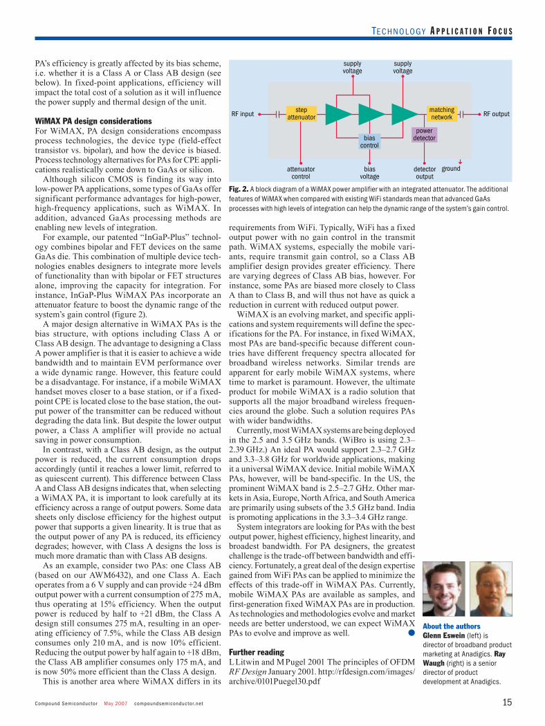
As the deployment of fixed WiMAX moves for-ward, the trend is to use higher output power from the PA. This is driving the industry to create better PAs. For instance, Anadigics’ AWM6432 power amplifier module (figure 1) is currently being used in WiMAX customer premises equipment (CPE) to deliver a typical output power of +24 dBm from the PA (or 21–22 dBm at the antenna) with a 2.5% or better EVM. While this level of performance is sufficient for most CPE applications, many designers are looking for PAs with +27 dBm output power or more, in order to dis-tinguish their products from the competition.
The best PAs will have an optimized combination of linearity (in terms of output power) and efficiency. In mobile WiMAX, PA efficiency is especially cru-cial because it has a direct impact on battery life. The
Under pressure to get WiMAX products to market, it may be tempting to overlook the power amplifier, but designers who do so risk degrading system links and reducing battery life, say Glenn Eswein and Ray Waugh from Anadigics.
PA proves crucial in WiMAX designsR F I C s
Fig. 1. Anadigics’ AWM6432 power amplifier is designed for fixed-point WiMAX while, at February 2007’s 3GSM World Congress, the company launched a new product aimed at the mobile version of the technology.
Compound Semiconductor May 2007 compoundsemiconductor.net 15
Technol ogy A p p l i c A t i o n F o c u s
PA’s efficiency is greatly affected by its bias scheme, i.e. whether it is a Class A or Class AB design (see below). In fixed-point applications, efficiency will impact the total cost of a solution as it will influence the power supply and thermal design of the unit.
WiMAX PA design considerationsFor WiMAX, PA design considerations encompass process technologies, the device type (field-effect transistor vs. bipolar), and how the device is biased. Process technology alternatives for PAs for CPE appli-cations realistically come down to GaAs or silicon.
Although silicon CMOS is finding its way into low-power PA applications, some types of GaAs offer significant performance advantages for high-power, high-frequency applications, such as WiMAX. In addition, advanced GaAs processing methods are enabling new levels of integration.
For example, our patented “InGaP-Plus” technol-ogy combines bipolar and FET devices on the same GaAs die. This combination of multiple device tech-nologies enables designers to integrate more levels of functionality than with bipolar or FET structures alone, improving the capacity for integration. For instance, InGaP-Plus WiMAX PAs incorporate an attenuator feature to boost the dynamic range of the system’s gain control (figure 2).
A major design alternative in WiMAX PAs is the bias structure, with options including Class A or Class AB design. The advantage to designing a Class A power amplifier is that it is easier to achieve a wide bandwidth and to maintain EVM performance over a wide dynamic range. However, this feature could be a disadvantage. For instance, if a mobile WiMAX handset moves closer to a base station, or if a fixed-point CPE is located close to the base station, the out-put power of the transmitter can be reduced without degrading the data link. But despite the lower output power, a Class A amplifier will provide no actual saving in power consumption.
In contrast, with a Class AB design, as the output power is reduced, the current consumption drops accordingly (until it reaches a lower limit, referred to as quiescent current). This difference between Class A and Class AB designs indicates that, when selecting a WiMAX PA, it is important to look carefully at its efficiency across a range of output powers. Some data sheets only disclose efficiency for the highest output power that supports a given linearity. It is true that as the output power of any PA is reduced, its efficiency degrades; however, with Class A designs the loss is much more dramatic than with Class AB designs.
As an example, consider two PAs: one Class AB (based on our AWM6432), and one Class A. Each operates from a 6 V supply and can provide +24 dBm output power with a current consumption of 275 mA, thus operating at 15% efficiency. When the output power is reduced by half to +21 dBm, the Class A design still consumes 275 mA, resulting in an oper-ating efficiency of 7.5%, while the Class AB design consumes only 210 mA, and is now 10% efficient. Reducing the output power by half again to +18 dBm, the Class AB amplifier consumes only 175 mA, and is now 50% more efficient than the Class A design.
This is another area where WiMAX differs in its
requirements from WiFi. Typically, WiFi has a fixed output power with no gain control in the transmit path. WiMAX systems, especially the mobile vari-ants, require transmit gain control, so a Class AB amplifier design provides greater efficiency. There are varying degrees of Class AB bias, however. For instance, some PAs are biased more closely to Class A than to Class B, and will thus not have as quick a reduction in current with reduced output power.
WiMAX is an evolving market, and specific appli-cations and system requirements will define the spec-ifications for the PA. For instance, in fixed WiMAX, most PAs are band-specific because different coun-tries have different frequency spectra allocated for broadband wireless networks. Similar trends are apparent for early mobile WiMAX systems, where time to market is paramount. However, the ultimate product for mobile WiMAX is a radio solution that supports all the major broadband wireless frequen-cies around the globe. Such a solution requires PAs with wider bandwidths.
Currently, most WiMAX systems are being deployed in the 2.5 and 3.5 GHz bands. (WiBro is using 2.3–2.39 GHz.) An ideal PA would support 2.3–2.7 GHz and 3.3–3.8 GHz for worldwide applications, making it a universal WiMAX device. Initial mobile WiMAX PAs, however, will be band-specific. In the US, the prominent WiMAX band is 2.5–2.7 GHz. Other mar-kets in Asia, Europe, North Africa, and South America are primarily using subsets of the 3.5 GHz band. India is promoting applications in the 3.3–3.4 GHz range.
System integrators are looking for PAs with the best output power, highest efficiency, highest linearity, and broadest bandwidth. For PA designers, the greatest challenge is the trade-off between bandwidth and effi-ciency. Fortunately, a great deal of the design expertise gained from WiFi PAs can be applied to minimize the effects of this trade-off in WiMAX PAs. Currently, mobile WiMAX PAs are available as samples, and first-generation fixed WiMAX PAs are in production. As technologies and methodologies evolve and market needs are better understood, we can expect WiMAX PAs to evolve and improve as well.
Further readingL Litwin and M Pugel 2001 The principles of OFDM RF Design January 2001. http://rfdesign.com/images/archive/0101Puegel30.pdf
supply voltage
supply voltage
detector output
bias voltage
attenuator control
ground
RF outputRF input step attenuator
bias control
power detector
matching network
Fig. 2. A block diagram of a WiMAX power amplifier with an integrated attenuator. The additional features of WiMAX when compared with existing WiFi standards mean that advanced GaAs processes with high levels of integration can help the dynamic range of the system’s gain control.
About the authorsGlenn Eswein (left) is director of broadband product marketing at Anadigics. Ray Waugh (right) is a senior director of product development at Anadigics.
compoundsemiconductor.net May 2007 Compound Semiconductor16
Technology I I I – V L o g I c
Despite the recent application of high-k dielectrics and metal gates in volume CMOS processes, and the scattergun approach to logic devices based on III–V materials, the compound and silicon industries have much in common. Bob Metzger looks at post-CMOS convergence.
High-k gate stacks point towards digital convergence
Some in the III–V world may have taken recent news from Intel and IBM about their individual develop-ments of highly insulating materials (high-k dielec-trics) and metal gates in place of SiO2 as bad news for digital applications of GaAs. On the face of it, it might have seemed that compound efforts could become redundant if CMOS is able to continue scaling.
But those who have been working with III–Vs for digital IC applications are quick to disagree. Jesus del Alamo at MIT, who has been investigat-ing the use of AlInAs/InGaAs HEMTs on InP for digital IC applications, said: “The announcements from Intel and IBM are not entirely unexpected. It was clear that high-k dielectrics would eventually show up, and this does not really change things. The current view is that silicon will run out of steam around the 22 nm node [post-2011] and that new materials will be required.”
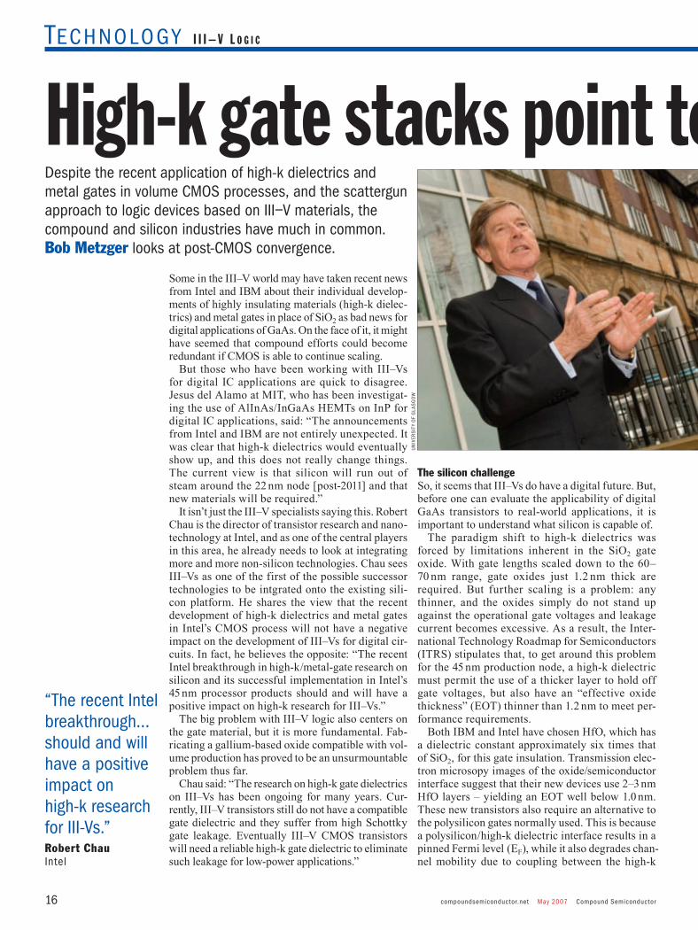
It isn’t just the III–V specialists saying this. Robert Chau is the director of transistor research and nano-technology at Intel, and as one of the central players in this area, he already needs to look at integrating more and more non-silicon technologies. Chau sees III–Vs as one of the first of the possible successor technologies to be intgrated onto the existing sili-con platform. He shares the view that the recent development of high-k dielectrics and metal gates in Intel’s CMOS process will not have a negative impact on the development of III–Vs for digital cir-cuits. In fact, he believes the opposite: “The recent Intel breakthrough in high-k/metal-gate research on silicon and its successful implementation in Intel’s 45 nm processor products should and will have a positive impact on high-k research for III–Vs.”
The big problem with III–V logic also centers on the gate material, but it is more fundamental. Fab-ricating a gallium-based oxide compatible with vol-ume production has proved to be an unsurmountable problem thus far.
Chau said: “The research on high-k gate dielectrics on III–Vs has been ongoing for many years. Cur-rently, III–V transistors still do not have a compatible gate dielectric and they suffer from high Schottky gate leakage. Eventually III–V CMOS transistors will need a reliable high-k gate dielectric to eliminate such leakage for low-power applications.”
The silicon challengeSo, it seems that III–Vs do have a digital future. But, before one can evaluate the applicability of digital GaAs transistors to real-world applications, it is important to understand what silicon is capable of.
The paradigm shift to high-k dielectrics was forced by limitations inherent in the SiO2 gate oxide. With gate lengths scaled down to the 60–70 nm range, gate oxides just 1.2 nm thick are required. But further scaling is a problem: any thinner, and the oxides simply do not stand up against the operational gate voltages and leakage current becomes excessive. As a result, the Inter-national Technology Roadmap for Semiconductors (ITRS) stipulates that, to get around this problem for the 45 nm production node, a high-k dielectric must permit the use of a thicker layer to hold off gate voltages, but also have an “effective oxide thickness” (EOT) thinner than 1.2 nm to meet per-formance requirements.
Both IBM and Intel have chosen HfO, which has a dielectric constant approximately six times that of SiO2, for this gate insulation. Transmission elec-tron microsopy images of the oxide/semiconductor interface suggest that their new devices use 2–3 nm HfO layers – yielding an EOT well below 1.0 nm. These new transistors also require an alternative to the polysilicon gates normally used. This is because a polysilicon/high-k dielectric interface results in a pinned Fermi level (EF), while it also degrades chan-nel mobility due to coupling between the high-k
“The recent Intel breakthrough…should and will have a positive impact on high-k research for III-Vs.”Robert ChauIntel
Compound Semiconductor May 2007 compoundsemiconductor.net 17
Technology I I I – V L o g I c
High-k gate stacks point towards digital convergence
dielectric and the inversion charge in the channel. Intel is using individual metal gates for the PMOS and NMOS (p-channel and n-channel) devices to solve this problem. Those metals, whose exact com-positions remain a secret, can be used to adjust indi-vidual threshold voltages.
When compared with the prior generation of polysilicon/SiO2 transistors, the new materials improve drive current by 20% and reduce source-drain leakage current by a factor of five. They will be used in the quad-core version of Intel’s next-generation “Penryn” processor, which will contain 800 million transistors.
One can make an educated guess as to how this device may evolve. Biaxially-strained active sili-con layers on top of a relaxed SiGe layer could be employed to alter bandstructure and improve mobil-ity, for instance. But even if such a device is pushed to its theoretical limit, the ITRS forecasts that when gate dimensions reach 14 nm, CMOS will hit a fun-damental technology roadblock. This is expected around the year 2020.
The III–V opportunitySo, if this is where the opportunity for III–V logic lies, what are the realistic options and what has been achieved so far? To answer those questions, we need to take a close look at some of the fundamental con-cepts that underpin all digital electronics.
Transistors can be operated in either enhancement mode (E-mode) or depletion mode (D-mode). An
E-mode device requires a gate voltage to be turned on. D-mode transistors are naturally “on” and are switched off by a gate voltage (see figure 1).
For many, the E-mode NMOS device is syn-onymous with the formation of an inversion layer. From a more fundamental perspective, it is simply a device that turns on with a positive applied voltage. This may seem trivial, but the distinction is critical when considering the various E-mode III–V-based devices under development for digital applications.
For silicon, high-quality SiO2 permits both NMOS and PMOS type devices – the two funda-mental building blocks of digital circuitry. The key is that the NMOS and PMOS devices can be com-bined in the fabrication of fast, efficient ICs through CMOS processing.
Unfortunately, the lack of a high-quality, native III–V oxide has seriously hampered logic transistor development in GaAs. It has limited the fabrication of rectifying junctions to p–n and Schottky junctions only. As a result, the typical digital GaAs device is the MESFET, in which the gate is formed by a rectifying Schottky metal-semiconductor junction. While able to hold off significant reverse biases, this junction will pass significant currents at small forward biases. This property limits the implemen-tation of MESFETs in logic applications to small (500 mV) voltage swings dictated by the Schottky gate structure. Although very fast MESFET logic has been developed, the approach requires complex layouts and consumes excess power.
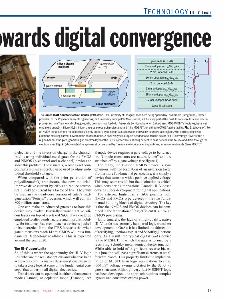
silicon dioxide(insulator)
metal tracks
source gate drain
n-channel
n-typesiliconp-type silicon
gate electrode
silicon substrate
gate oxide (κ = 20)
2 nm undoped AL0.45Ga0.55As
2 nm undoped GaAs
10 nm undoped In0.3Ga0.7As
2 nm undoped GaAs
3 nm undoped Al0.3Ga0.7As
65 nm undoped Al0.3Ga0.7As
0.2 µm undoped GaAs buffer
GaAs SI substrate
EF EC
The James Watt Nanofabrication Centre (left) at the UK’s University of Glasgow, seen here being opened by Lord Broers (foreground), former president of the Royal Academy of Engineering, and university principal Sir Muir Russell, will be a key part of the push to converge III–V and silicon processing. Iain Thayne and colleagues, who previously worked with Freescale Semiconductor on GaAs-based MOS-PHEMT structures, have just embarked on a £4 million ($7.9 million), three-year research project entitled “III-V MOSFETs for ultimate CMOS” at the facility. Fig. 1. (above left) For an NMOS enhancement-mode device, a lightly doped p-type region exists between the two n+ source/drain regions, with the resulting n+/p junctions blocking current flow from the source to drain. A positive gate voltage is needed to switch the device “on”. This voltage “inverts” the p-region beneath the gate, generating an electron layer at the Si–SiO2 interface, enabling current to pass between the source and drain through the electron layer. Fig. 2. (above right) The epilayer structure used by Freescale to fabricate an implant-free, enhancement-mode GaAs MOSFET.
compoundsemiconductor.net May 2007 Compound Semiconductor18
Technology I I I – V L o g I c
This inherent weakness, in particular for E-mode n-channel devices, has driven the search for a compatible oxide that would eliminate the need for Schottky junctions and allow fabrica-tion of a true III–V CMOS hybrid. Until recently, that search had been largely fruitless, and even today the best of these devices remain at the early research stage.
Researchers from Kanazawa University in Japan obtained one of the best results in 2004. They formed an oxi-nitride gate dielectric using ozone oxidation and a nitrogen gas plasma. The result was an n-channel E-mode GaAs MOSFET with a threshold voltage of 0 V and a claimed transcon-ductance of 50 mS/mm (see Tametou et al. 2004). It represented a major breakthrough for inversion-mode GaAs MOSFETs, because the transconduc-tance was nearly two orders of magnitude greater than anything previously reported. While impres-sive, this transconductance figure remains signifi-cantly lower than that of a basic NMOS device.
Fortunately, there is another path to making E-mode MOSFETs in GaAs – one that does not rely on the generation of an inversion charge at the semi-conductor–dielectric interface.
Led by Matthias Passlack, researchers at Freescale Semiconductor have developed a non-inversion-type E-mode MOSFET – in other words, a MOS-PHEMT hybrid (see figure 2, p17, for the epilayer design and the bandstructure). In this approach, the epilayers beneath the MOS portion of the device form an InGaAs strained channel (see Passlack et al. 2006 and 2007). The transistor dielectric consists of an amorphous layer of Ga2O3/GdGaO. The Ga2O3, which sits at the semiconductor–dielectric interface, is just three or four monolayers thick, and GdGaO forms the remainder of the high-k dielectric. With a dielectric constant of 20, GdGaO behaves like a thinner version of SiO2.
Unlike a conventional PHEMT, where threshold voltage is set by the depth of the gate recess etch, in the MOS-PHEMT hybrid this property is deter-mined by the thickness of the dielectric layer and its distance from the channel, as well as the gate metal work-function. The geometry of the gate and
the underlying epilayers also distance the channel from the semiconductor–dielectric interface (see figure 3).
In collaboration with researchers at the Nanoelec-tronics Research Centre (now the James Watt Nano-fabrication Centre) at the University of Glasgow in the UK, Freescale fabricated E-mode devices with 1 µm gate-lengths and dielectric layers ranging from 10 to 18 nm thick. The resulting transistors had a threshold voltage of 0.28 V, a maximum drain current of 397 mA/mm and a maximum transcon-ductance of 428 mS/mm.
Although they are an order of magnitude better than the Japanese group’s GaAs MOSFETs, these results are close to what one would expect for a GaAs PHEMT utilizing a similar channel struc-ture. At first glance, therefore, this device might be viewed almost as a regular PHEMT – albeit one in which the threshold voltage is dictated by the geom-etry of the dielectric layer rather than the depth of the recess etch. However, the Ga2O3/GdGaO dielec-tric has done more than simply set the threshold voltage: it has eliminated the problematic metal-gate Schottky layer.
Now, let’s take a closer look at the InGaAs/InP devices that Jesus del Alamo and his MIT team have been working on, which, at first, appeared to highlight a rather different approach. Although these devices scale well to gate lengths of 100 nm, serious short-channel effects then begin to appear – including shifts in threshold voltage as a function of gate length, and drain-induced barrier lower-ing. However, these effects can be reduced dra-matically by thinning the AlInAs Schottky layer to 3.0 nm, making 50–60 nm gate-length devices perfectly feasible.
But – just like SiO2 – AlInAs Schottky layers less than 3 nm thick begin to exhibit excessive leakage. Drain currents become dominated by charge pass-ing from the gate into the channel, and the transis-tors become useless. “This is the key limitation for scaling and the need for a high-k dielectric to allow future scaling is very clear,” said del Alamo. The solution, and the future device that he envisages is, in fact, of the same type as Freescale’s – the hybrid MOS-PHEMT.
Intel not only sponsors del Alamo’s work – it is actively involved in the development of even more exotic III–V devices and potential dielectrics for digital applications. Working with Qinetiq in Mal-vern, UK, its researchers have fabricated 85 nm InSb channel PHEMTs in both E-mode and D-mode form, where the threshold voltage is determined by the depth of the recess etch (see Datta et al. 2005 and Chau 2006).
The InSb material system exhibits the highest electron mobility and saturation velocity of any known semiconductor, and Intel is aiming to develop a future generation of very-low-power logic devices with a VDS of only 0.5 V. Chau and his researchers are also investigating possible dielectrics to replace
normally on normally off
gate oxide
sour
ce
drain
semi-insulating substrate
VG = 0 V
gate
epitaxiallayers
EFEc EcEF
gate oxide
sour
ce
drain
semi-insulating substrate
VG = Von
gate
epitaxiallayers
EFEc EcEFEF
normally on normally off
gate oxide
sour
ce
drain
semi-insulating substrate
VG = 0 V
gate
epitaxiallayers
EFEc EcEF
gate oxide
sour
ce
drain
semi-insulating substrate
VG = Von
gate
epitaxiallayers
EFEc EcEFEF
Fig. 3. Under flatband conditions (a), the channel in the source-gate and gate-drain access regions of the Freescale transistor are “on” without an applied gate voltage, while the channel region beneath the gate is “off”. When a positive gate voltage is applied (b), the Fermi level (EF) is pulled up into the conduction band (EC) beneath the gate, and the channel is switched “on”.
Compound Semiconductor May 2007 compoundsemiconductor.net 19
Technology I I I – V L o g I c
About the authorBob Metzger ([email protected]) is a freelance journalist based in Chapel Hill, NC.
the Schottky gate, and they have found that Al2O3 can reduce gate leakage into the channel by six orders of magnitude.
ConvergenceWhat all of this work is pointing to is an increasing convergence of approaches to find the best digital IC platform for a post-CMOS industry. Whether research teams are focused on III–V or silicon, all are envisioning a device that merges the best of both worlds. In other words: a channel region taking advantage of the superior transport characteristics of high mobility III–V materials, combined with a metal-gate/high-k dielectric to allow device scaling well into the sub-50 nm region.
Efforts to optimize the pairing of high-k gate dielectrics with the underlying semiconductor will now begin, with teams seeking combinations that will minimize the number of traps and defects at the semiconductor interface and the negative interac-tion with charge in the channel, while maintaining low gate-leakage currents.
MBE specialist David Braddock, CEO of OSEMI in Rochester, supplied the initial Ga2O3/GdGaO dielectric stacks on GaAs to Freescale. He sees the common ground between this approach and the efforts at MIT, Intel and elsewhere. “High-k dielec-tric gate stacks for compound semiconductors is the
real enabling technology,” he said.But when Braddock looks at this convergence,
his compound material of choice is different again. Alongside Mark Johnson and Doug Barlage at North Carolina State University, Braddock has considered the nitride system as a strong candidate for merg-ing with high-k dielectrics. According to him: “In the case of GaN, gallium oxides may be mixed with hafnium and gadolinium oxides to form strained oxide layers with low border trap densities and low interface state densities.”
Although precisely which III–V materials and high-k dielectrics will end up being used remains an open question, a common vision is beginning to emerge – one shared by key figures in both III–V and silicon. It is a convergence of the best of both worlds that will carry digital ICs beyond the CMOS era.
Further readingR Chau Challenges and opportunities of nanoelec-tronics for future logic applications 2006 Device Research Conference.S Datta et al. 2005 IEDM Technical Digest 763.M Passlack et al. 2006 IEEE Transactions on Elec-tronic Devices 53 10 2454.M Passlack et al. High mobility III–V MOSFET technology (to be presented) CS ManTech 2007.M Tametou et al. 2004 IPRM Proc. 187.
Compound Semiconductor May 2007 compoundsemiconductor.net 21
Technology I n f r a r e d d e t e c t o r s
Infrared imaging systems have several advantages over their optical equivalents. They can operate at night, because image contrast is solely provided by temperature differences, and they can work in poor weather conditions by detecting radiation in particular wavelength bands. Image quality is also less affected by reflections from sunlight and emission from bright light sources, such as car headlights, particularly when the detection band in the 8–12 µm range is selected.
As a result, these semiconductorbased imagers are suitable for a wide variety of everyday uses. However, cost has limited their deployment to military and space applications, where they are predominantly used for surveillance and targeting of hot objects, such as rockets and vehicle motors.
The military’s use of these detectors began in the 1970s with firstgeneration cameras featuring cooled, small linear arrays of photodetectors coupled to a complex twodimensional scanning system. By the 1980s secondgeneration versions, which included a readout integrated circuit for signal preprocessing and multiplexing on the focal plane, had been built in research labs. These were then commercialized in the early 1990s.
The progression to secondgeneration detectors opened the way for highresolution scanned arrays featuring time delay and integration, and highresolution twodimensional arrays with signal processing on the focal plane. Cooled “staring” twodimensional arrays operating in the medium and longwavelength infrared bands were also developed, which have been dubbed “2.5generation” infrared detectors. These imagers, which were launched commercially in the late 1990s, have arrays with typically 320 × 256 or 640 × 512 pixels, and are suitable for applications such as missile detection. The improved resolution and performance of all these secondgeneration detectors have doubled the effective range for target acquisition, and enabled identification of enemy vehicles at night through smoke and dust at distances of 6 km and more.
These various generations of infrared imagers have been fabricated with a variety of tech
nologies, and include detector arrays made from HgCdTe, InSb, InGaAs and GaAs quantum wells (see figure 1, p22, for an overview). Each of these detectors has particular merits, and selection is application specific.
The performance of these detectors can be evaluated by their ability to distinguish a small target from an infrared background with a similar temperature. Military, security and surveillance applications use this as a test, and rate the imagers’ performance in terms of detection or identification range, and ability to deal with adverse weather.
The highest class of detectors can image objects at distances of 10 km or more, depending on atmospheric conditions and altitude, and are suitable for many different applications. These include missile guidance and tracking, missile warning, providing tank and airborne vision enhancement, carrying out reconnaissance and climate observations, agricultural monitoring, pollution analysis, and astronomical observations. Comparable detectors with an operating range of 6–10 km can also be used for scientific applications, including analysis of relatively weak signals for gas spectroscopy.
The detectors that operate over these ranges
For decades, infrared detector development has drawn on many different types of compound semiconductor material. Philippe Tribolet explains why Sofradir has selected HgCdTe for its future plans. These include building a new $12 million fab to cut chip manufacturing costs, which should ultimately lower detector prices and drive up sales of these high-specification imagers.
Sofradir builds a new factory to ramp HgCdTe chip production
Infrared imagers can be used for a wide variety of applications, but high costs tend to limit their use to military and space applications, such as tracking tank movements at night.
compoundsemiconductor.net May 2007 Compound Semiconductor22
Technology I n f r a r e d d e t e c t o r s
require cooling, and are predominantly based on HgCdTe and InSb chips. HgCdTe has several advan-tages (see box “The strengths of HgCdTe”), includ-ing a sensitivity over a spectral range stretching from visible wavelengths to 18 µm, a high quantum efficiency coupled to a high signal-to-noise ratio, and a relatively high operating temperature that reduces the cost of the associated cooler. LPE has been used for many years to produce these chips, but single- and dual-band chips covering short-wave (1–3 µm) and medium-wave (3–5 µm) infrared bands can now be produced in large volumes and at low costs using MBE.
By comparison, InSb is only sensitive in the medium-wave infrared band (3–5 µm). Technologi-cal limitations also hinder improvements in operat-ing temperature and very small pixel sizes, making this material unsuitable for the most demanding applications. Alternative technologies include quan-tum-well infrared photodetectors (QWIPs), which can be used for long-range detection (8–12 µm) but have slow frame rates and require lower operating temperatures, and type II superlattices, which are still under development.
Another class of detectors are those with a 2–6 km detection range. These can serve civilian needs such as fire surveillance; security applications such as police surveillance and tracking, border surveil-lance, and airborne landing vision enhancement; and also provide imaging in military small armored vehicles and certain types of unmanned airborne vehicles. Cooling the detector is mandatory in all these applications. In some cases the selection of a very high-performance detector can actually cut the overall system cost, as this can reduce the size of the optics, simplify the signal processing and ease reliability constraints.
The candidates for providing infrared detection over these distances are similar to those for the longer ranges. However, QWIPs operating in the infrared long-wavelength band can offer good value for money if their limited efficiency and relatively
high dark current can be tolerated. InGaAs cameras operating at shorter wavelengths are also competi-tive, but they can suffer from read-out circuit noise when the input signal is low, and they cannot detect beyond 1.9 µm.
The final class of detectors are those used for imag-ing objects at distances between tens of meters and 2 km. They can also serve civilian applications, such as building inspection, industrial process control, industrial site surveillance, and automotive driving enhancement, and other uses will emerge as the cost of these detectors fall. Uncooled thermal detectors, such as micro-bolometers, which include imagers based on amorphous silicon that is fully compatible with CMOS silicon technologies, offer the best value for money and are best suited to these tasks.
The French legacyMany of these different types of chip-based detec-tors have been commercialized in France, a country with a very strong history of infrared detector devel-opment. Currently over 500 people are employed for the research, advancement, and manufacture of these devices in the Grenoble area, which makes this region a major global player in this technology.
The research has been led by the national research and development center CEA-Leti, which started developing infrared detectors in the 1970s. This knowledge has been transferred to Sofradir, which is headquartered in Chatenay-Malabry and has production facilities in Veurey-Voroize. The research from CEA-Leti has been used in our production of second- and 2.5-generation detec-tors, which we have been manufacturing for over 13 years, and the amorphous silicon micro-bolometers that we have been building since 2003 through our subsidiary, ULIS. QWIPs developed at Thales Research and Technologies (TRT), France, are also being mass-produced in cooperation with us, and InSb and InGaAs technologies are being developed within France.
Today, we are manufacturing thousands of cooled
Sofradir’s current products include a second generation “Scorpio” detector that contains a chip grown by LPE on 2 inch CdZnTe, which features 640 × 512 pixels with a 15 µm pixel pitch. The new MBE fab will be used to produce additional products, such as a third generation of detectors with multicolor capability.
Fig.1. (left) HgCdTe detectors grown by MBE and LPE deliver better object-identification capability than thermal detectors, such as micro-bolometers, and those based on InGaAs and InSb. Fig .2. (right) Switching from CdZnTe substrates to those made from germanium can substantially boosts the number of die per wafer. Sofradir will be making this transition following the completion of its new factory. Further scaling is also possible, as 6 inch germanium is available commercially, and the feasibility of production at even larger diameters has been demonstrated by substrate manufacturers.
Compound Semiconductor May 2007 compoundsemiconductor.net 23
Technology I n f r a r e d d e t e c t o r s
infrared detectors, alongside tens of thousand uncooled detectors through ULIS. In addition, we are currently building a new €9 million ($12.1 mil-lion) MBE fab for HgCdTe chip production, which will scale up our production from 2 inch to 4 inch material. When installation is completed in summer 2008, the increases in manufacturing volumes and efficiencies will reduce our production costs and also enable us to make larger chips. In addition, the lower costs should have an effect on the price of the longer-range detectors that will employ our chips, and should drive an increase in sales of this type of imager. One-third of the cost of an infrared detec-tor is associated with the focal-plane array, so lower chip manufacturing costs can have a big impact on the price of the overall system.
Third-generation detectorsOur new fab will be used to mass-produce third-generation detectors that have been developed in-house. These devices provide multicolor operation, have large focal-plane arrays with homogenous active layers, can resolve more image detail and operate more effectively in poor weather.
The chips will be produced by MBE, a technique capable of growing the multiple layers required by multicolor detectors on a wide variety of large-diameter substrates. This replaces our current growth technique used for production, LPE, which is carried out on lattice-matched CdZnTe sub-strates. These substrates are only available in small sizes, so many fabs are now developing silicon or GaAs platforms that offer low cost and a compat-ibility with the thermo-mechanical characteristics of the read-out circuit. In France, however, germa-nium has been the preferred alternative, because the lower stability of its oxides makes its surface easier to prepare, both ex situ and in situ, prior to MBE growth.
The MBE process on germanium (211) was demonstrated several years ago at CEA-Leti, and
is suitable for making larger arrays. This sub-strate is already available in 4 inch and larger ver-sions, which can be used to make the high-quality HgCdTe films needed for two-dimensional short-wavelength and medium-wavelength infrared arrays. We plan to start mass-producing both of these types of arrays during summer 2008, using two MBE reactors with a 1 × 4 inch and a 3 × 4 inch capacity. The switch to a larger wafer size will give us an advantage over InSb and QWIP manufactur-ers, who are still using 3 inch substrates for mass-production (see figure 2). In addition, it will allow us to affordably fabricate 1280 × 1024 pixel infra-red focal-plane arrays with a 15 µm pixel pitch that will provide a greater image identification capabil-ity than detectors with fewer pixels.
We are also continuing to improve our third- generation detectors, so that manufacturing costs can be cut and selling prices reduced. In particu-lar, we are focusing on the development of smaller pixel pitches and larger formats, and improving the performance of our avalanche photodiodes (APDs) and multicolor detectors. Our HgCdTe APDs are a unique design based on electron-impact ionization, and deliver exceptional detection. These electron initiated APDs deliver a thousandfold multiplica-tion gain at an inverse bias of only 10 V. The high gain at low bias, combined with a low noise factor, makes these APDs particularly well-suited for integ-ration in the latest FPAs. These are ideal for active laser-based imaging, but they can also serve many passive imaging applications.
Our continual development of HgCdTe for a wide variety of focal-plane arrays will lead to fabrica-tion of a series of very high performance detectors. These devices, which will outperform detectors fabricated with competing technologies, will ben-efit from the use of electron initiated APDs. With this technology we can meet our customers’ needs for greater performance, lowered system cost or fewer constraints.
About the authorPhilippe Tribolet ([email protected]) is Sofradir’s vice-president of R&D, technologies and products. He directs production programs for French and international military, aerospace and security customers. The work carried out by his team of 80 engineers and technicians includes HgCdTe growth, and the design of silicon integrated circuit components.
HgCdTe has intrinsic characteristics that make it ideal for use in infrared detectors. Its main advantage is the wide tuning range of its bandgap – possible through changes in composition (see figure). This tuning is possible without introducing significant strain into the alloy, as CdTe and HgTe have similar lattice constants. Comparable lattice constants also enable the growth of multilayer structures with few defects and dislocations. Another strength of HgCdTe is its long carrier lifetime, which leads to a low dark current and enables the fabrication
of photodiodes with a quantum efficiency approaching 100%.
The combination of favorable material characteristics, in conjunction with the commercial availability of suitable substrates such as CdTe and HgCdTe, enables the fabrication of a large variety of infrared detectors, including multicolor versions. Imagers can also be built using backside illumination through a thinned substrate that can block out near ultraviolet and visible radiation without decreasing the detector’s quantum efficiency.
The strengths of HgCdTe
Adjusting the composition of HgCdTe produces massive changes in this material’s bandgap. At a composition of Hg0.85Cd0.15Te the material has zero bandgap and is actually a semimetal.
Whatever your inspiration, STS takes your ideas further. As a keyprovider of plasma etch and deposition technologies for over 20years, STS continues to deliver expert knowledge and advancedthinking to customers based on proven technology.
Whether you are an emerging or established enterprise we offerunrivalled experience, and unparalleled knowledge of our proventechnologies turning your innovations into reality. Above all, we listen to our customers. Their success is all the inspiration we need.To find out more visit: www.stsystems.com
Compound Semiconductor May 2007 compoundsemiconductor.net 25
Technology E q u i p m E n t u p d a t E
Profitable chip making demands low development costs and high production yields. To cut expense, growth recipes should be established using minimal runs, because this optimization process can consume a large proportion of the development budget. To do this, process engineers must know as much as pos-sible about the reactor’s local environment, includ-ing wafer temperature – a primary driver of epilayer growth rates and compositions.
Pyrometry is the standard method for measuring the wafer’s temperatures within a reactor. The technique involves measuring the intensity of thermal radiation emitted by the wafers over a narrow wavelength band using a photodetector, and then correlating this inten-sity to a temperature. The temperature of wafers based on InP and GaAs material systems can be measured with a pyrometer operating at 950 nm. However, this spectral region is useless for nitrides, because they do not produce any radiation at this wavelength.
To address this deficiency, pyrometers that oper-ate at 400 nm have been built for nitride growth. The first of these was constructed by J Randall Creighton and co-workers from Sandia National Laboratories, NM, and last year in situ monitoring specialist Lay-Tec introduced a commercial version of this tool, the Pyro 400, at the MRS fall meeting in Boston, MA. This instrument is primarily designed for Aix-tron multi-wafer reactors, but could be adapted for Thomas Swan tools.
Developing a pyrometer that operates in the near ultraviolet is not easy, according to LayTec’s presi-dent Thomas Zettler: “In a reactor at 1000 C there is very intense radiation at all wavelengths, and it’s a real challenge to measure 400 nm emission accu-rately.” Emission at 400 nm is many orders of magni-tude weaker than infrared radiation, and the careful selection of several filters is required to block out this unwanted radiation. Operating in this wavelength range enables LayTec’s instrument, which consists of collection optics, filters and a detector, to measure the surface temperature of multiple wafers with a
precision of ±0.1 C or less. Such precision exceeds that of all other commercial tools, says Zettler.
Although the Pyro 400 can measure temperatures with very high precision, it does not feature emissiv-ity correction. This means that it ignores the varia-tions in emissivity between different objects, and that the growth of an anti-reflection film would produce a change in the value of the recorded temperature. However, Zettler believes that this weakness is not a big deal. That’s because the tool is primarily designed to check bare wafer surface temperature, and there is also only a small difference between the emissitivi-ties of GaN and AlN.
To drive sales, Laytec will have to convince its cus-tomers to add the Pyro 400 to other in situ instruments already installed in reactors, such as laser deflection and reflectance tools that monitor surface bowing and susceptor surface temperature. These monitors can ensure wafer flatness, but they cannot reveal whether temperature variations occurred across the substrate during the growth. These differences can exist even before growth begins, says Zettler, as they can come from slight variations in the susceptor’s geometry.
Zettler believes that the Pyro 400 can deliver the greatest benefit as a complementary tool to LayTec’s Epicurve TT sensors during the development of growth recipes for future products. These recipes must pro-duce wafers with uniform, high-quality active regions and a low degree of bowing. The number of runs required to fine-tune this growth can be reduced with the pyrometer, says Zettler, adding that the in-house expertise generated from developing the instrument has also enabled the company to show customers how to get more out of its wafer-bowing equipment.
At the MRS meeting, Zettler’s colleague Elizabeth Steimetz presented a poster detailing the capabilities of the Pryo 400, which was co-authored by research-ers from the Ferdinand Braun Institute for High Frequency Technology (FBH) in Berlin. The pyrom-eter was fitted to an Aixtron AIX2600HT planetary reactor equipped with LayTec’s EpiCurve sensor, and mapped the temperature of a platter containing 11 different 2 inch substrates and epiwafers with a preci-sion of ±0.1 C and a ± 3 mm spatial resolution.
These trials – which were conducted at 1100 C and a platter rotation speed of 6 rpm – revealed that a 10 µm bow caused by depositing GaN on sapphire produces a 4 C temperature variation across the wafer. Switching to a SiC platform replaces a con-vex bow with a concave one, and variations in wafer temperature decrease to 1.2 C per 10 µm of bow. According to the researchers, lowering the reactor’s temperature to 800 C and tuning the GaN nucle-ation layer growth with the Pyro 400 and a curva-ture sensor dramatically reduced the bowing of both of these epiwafers, leading to growth of quantum wells with excellent uniformity.
UV tool maps nitride temperaturesLayTec is targeting GaN chip developers with an in situ pyrometer that can measure wafer temperatures with a precision of ±0.1 °C. Richard Stevenson investigates.
M o c V d M o n i t o r
Nitride material does not emit thermal radiation at 950 nm, the conventional wavelength for MOCVD pyrometry, so temperature profiling is carried out at shorter wavelengths such as 400 nm.
“It’s a real challenge to measure 400 nm emission accurately.”Thomas ZettlerLaytec
Compound Semiconductor May 2007 compoundsemiconductor.net 27
Technology G a N L E D s
GaN LEDs are high-performance devices enjoying great commercial success. However, the science that underpins their operation is poorly understood, and an enthusiastic debate is currently raging within the scientific community to identify the basic mech-anism for light emission from these devices.
The debate is focused on why a GaN LED, and a GaN laser for that matter, can be an efficient emitter despite its very high defect density. In other material systems, such as GaAs, these two properties could not go hand in hand because such huge dislocation densities would cause swift and catastrophic failure through non-radiative carrier recombination at dis-location cores.
With GaN, however, bright emission and high reliability is commonplace, even when disloca-tion densities are as high as 1010 cm–2, seven orders of magnitude higher than those found in GaAs LEDs. These very high dislocation densities arise because GaN emitters are usually grown on for-eign substrates, such as SiC and sapphire, that have differing lattice constants. Although GaN bulk sub-strates can be produced, the process is incredibly challenging, and the crystals that are formed are currently too small and expensive for widespread commercialization.
To solve the GaN conundrum researchers throughout the community have analyzed the active region of typical devices, which contain several InGaN quantum wells approximately 2 nm thick sandwiched between GaN barriers. These experi-ments aimed to discover some form of microstruc-tural feature within the quantum wells that would be responsible for the efficient excitonic emission. Such a feature could potentially ensure high radia-tive efficiencies by preventing migration of elec-tron-hole pairs to non-radiative dislocation cores.
In the 1990s several researchers believed that they had found what they were looking for in trans-mission electron microscopy (TEM) images of the active region. Various micrographs revealed inhomogeneous strain contrast on a 2 – 3 nm scale in the quantum well, which was thought to result
from variations in the indium content along the well. These images led to a broad consensus con-cerning the mechanism of light emission from these structures, which was based on exciton localization at indium-rich clusters. These clusters ensured effi-cient light emission because the excitons were kept away from the radiation-quenching dislocations, unless a dislocation happened to pass through an indium-rich cluster.
The trouble with TEMHowever, these TEM images were not exactly what they seemed. When Tim Smeeton from our group at the Cambridge Centre for Gallium Nitride, UK, examined some InGaN quantum wells under mini-mal exposure to the electron beam, he found that the TEM images actually revealed rather uniform quantum wells. It was only after further exposure that inhomogeneous strain contrast could be seen (see figure 1). This led us to believe that these “indium clusters” observed in earlier TEM studies might be nothing more than measurement artefacts, and reopened the debate concerning the nature of localization in InGaN quantum wells.
Damaging the GaN sample by introducing defects
The popular theory for reconciling the excellent emission efficiency of GaN LEDs with their very high defect density is based on evidence of clustering in the InGaN quantum wells. But recent atom probe measurements have disproved this idea by showing that InGaN actually forms a random alloy, according to Mark Galtrey, Rachel Oliver, and Colin Humphreys from Cambridge University.
Atom probe provides evidence to question InGaN cluster theory
Fig. 1. TEM imaging can damage the sample under investigation, and introduce defects. Our TEM images of InGaN/GaN quantum wells taken after very little exposure to the electron beam (left) are significantly different to images taken from the same region after one minute’s exposure to the electron beam (right).
Erwin Müller invented the atomic probe technique in his laboratory at Pennsylvania State University in the late 1960s. The technique delivers chemical information with an atomic resolution by combining a time-of-flight mass spectrometer with a field ion microscope.
I N N O V A T I O NBBEEGGIINNSS WWIITTHH PPEEOOPPLLEE
Phone : +1-503-615-9000 • Fax : +1-503-615-8900 • E -mai l : foundry - in fo@tqs .com • Webs i te : w w w.t r iqu in t . com
Connecting the Digital Worldto the Global Network®
Meet Otto. His expertise helped make TriQuint the world’snumber one GaAs Foundry. With more than 25 years inprocess & microwave device development, Otto leads ourtechnology team, bringing exciting new high performance,cost-effective processes to the Foundry market. He helpedus offer the first commercial E/D pHEMT process: TriQuint’sTQPED. Otto’s team designed it to enable higher levelsof integration, reducing system-level manufacturing costs;just another way he puts customers first. Otto is one ofthe people behind the innovation at TriQuint Semiconductor,and he’s on your team.
Visit www.triquint.com/foundry and register for newproduct and process updates.
Compound Semiconductor May 2007 compoundsemiconductor.net 29
Technology G a N L E D s
is not the only weakness of TEM. In addition, the technique in its conventional form only allows struc-tures to be seen in projection, which means that the recorded image is a two-dimensional projection of a three-dimensional structure. Consequently, the application of a new technique that avoids electron-beam damage and delivers a fully three-dimensional set of data could be extremely beneficial.
The atom probe techniqueThe roots of such a technique were established over 50 years ago in the laboratory headed by Erwin Müller at Pennsylvania State University. On October 11, 1955 Müller and his team took the first ever atomic resolution image with the field ion microscope that he had invented. This instru-ment operates by ionizing the gas molecules that are above individual atoms located on the surface of a very sharp needle-shaped sample. This sample must be held at a high field, to ionize the gas, and at a very low temperature, to prevent gas molecules from moving across the surface and degrading the image’s resolution.
By 1968 Müller had discovered that atoms on the sample’s surface could be evaporated one at a time by superimposing a pulsed voltage onto the fixed one. Attaching a time-of-flight mass spectrometer to this instrument then allowed chemical identifi-cation of each atom. With this atomic resolution of chemical information, the atom probe was born. This instrument preceded the first atomic resolu-tion TEM pictures by two years, and the first scan-ning probe microscope measurements of individual atoms by more than two decades.
Despite these great successes, the atom probe was
not widely adopted. Various drawbacks plagued the first tools, such as slow collection rates, an extremely small field of view and the need for con-ducting samples. However, in recent years huge advances have been made in instrumentation. Fields of view of more than 100 × 100 nm are now possible, alongside detection rates exceeding a million atoms per minute. Pulsed lasers can also be used instead of pulsed voltages, enabling the atom probe to examine semiconducting and even insulating specimens.
Today, sample preparation is the greatest chal-lenge faced when using the atom probe. Samples must have a tip radius of 50 nm, and a region of interest located within a few hundred nanometers of the tip (see figure 2). For metallic samples, this is usually possible with electropolishing, but for many semiconductor samples a focused ion beam (FIB) instrument is the best tool. With this tech-nique, gallium ion beams can mill the sample to the correct shape, with platinum or tungsten protective layers being deposited to protect the sample from ion beam damage. Some instruments also com-bine a scanning electron microscope with the FIB column (a FIB/SEM). This enables imaging of the sample, which can help to ensure a good tip shape, and accurate positioning of the region of interest near to the tip.
Using the latest generation of atom probes (see figure 3), such as the local electrode atom probe from US-based Imago Scientific Instruments, enables three-dimensional reconstruction of the position and chemical identity of hundreds of mil-lions of atoms. Even elements present in very small concentrations, such as dopant atoms, can be easily detected and their distributions analyzed.
Fig. 2. (above right) Several processing steps are required to prepare samples for the atom probe microscope. The collection of images show (clockwise from top left): lifting out a thin membrane from a wafer using a micromanipulator; transferring a portion of the membrane on to a mounting wire; a sample ready for sharpening by annular ion beam milling; and a finished sample. Fig. 3. Measurements with a position-sensitive atom probe in Alfred Cerezo’s laboratory at the University of Oxford, UK, have revealed that InGaN quantum wells are a random alloy. Fig. 4. (right) The reconstruction of the quantum-well region of our sample, from the three-dimensional atomic probe data, shows the random alloy nature of InGaN. Only the gallium (blue) and indium (orange) atoms are displayed. The four quantum wells that were farthest from the surface of the wafer are clearly visible as indium-containing layers.
compoundsemiconductor.net May 2007 Compound Semiconductor30
Technology G a N L E D s
About the authorsColin Humphreys ([email protected]) is the Goldsmiths’ professor of materials science at the University of Cambridge, and the director of the Cambridge Centre for Gallium Nitride. Rachel Oliver (left) is a Royal Society university research fellow in the Department of Materials Science and Metallurgy at the University of Cambridge. Mark Galtrey (right) is a PhD student at the Cambridge Centre for Gallium Nitride.
Imaging quantum wellsWe have used an atom probe to search for nanometer-scale compositional variations in GaN-based quan-tum-well structures, and ultimately to determine whether or not nanometer-scale indium-rich clus-ters are needed for bright light emission. The atom probe is an ideal technique to answer this question because it avoids the major drawbacks of the TEM, and its only serious weakness is that the sample is consumed during the measurement.
The laser-pulsed atom probe has collected data from a small volume (20 × 20 × 100 nm) of a high-quality blue-emitting InGaN/GaN multiple quan-tum-well structure. Reconstructing this data clearly reveals the InGaN quantum-well layers (see figure 4). Measurements of the indium content in these lay-ers produced by atom probe agree to within 1% with compositions obtained by high-resolution X-ray dif-fraction, which is generally believed to be the most accurate method for determining composition.
To assess whether any clustering had occurred in the wells, we subdivided each layer into approxi-mately 1 nm-sized boxes and calculated the composi-tion of each box. If nanometer-scale indium-rich clusters had been present, we would have found that several of these boxes featured a much higher indium content than expected from a random alloy. In fact, we found that the distribution of the com-
position of the boxes fitted very well with that pre-dicted for a random alloy. In other words, there was no evidence for nanometer-scale indium-rich clus-ters in this sample, despite the fact that it emitted bright light.
Now that we have unequivocally demonstrated that indium-rich clusters are not a prerequisite for bright light emission, the conundrum returns: what is the mechanism for localization? Since GaN and its alloys have a very strong piezoelectric effect, slight variations in the quantum-well thickness could be sufficient to create local energy minima that localize the carriers. The atom probe can detect nanometer-scale interface roughness, and we plan to look for this in the future. However, possible uses for the atom probe in these systems go much further, extending from basic physics studies to analysis of practical devices. Since the FIB/SEM sample prepa-ration process is site-specific, material from failure points in LEDs could be tested to determine nano-scale changes associated with that failure. In short, this tool could provide the key to solving a whole range of problems that are fundamental to the suc-cess or failure of GaN-based light emitters.
Further readingM J Galtrey et al. 2007 Appl. Phys. Lett. 90 061903T M Smeeton et al. 2003 Appl. Phys. Lett. 83 5419
Compound Semiconductor May 2007 compoundsemiconductor.net 31
PMGI/LOR Resists for Lift-off ProcessingMicroChem CorpPMGI and LOR resists allow exceptionally good deposition control whenused as an undercut layer in bi-layer lift-off processing. PMGI resists areideally suited for high resolution (sub 0.25 µm) lift-off processes, whileLOR resists are better suited for thick >1 um) metal deposition processes.Both products permit easy process tuning, high yields, superior deposition
line width control and are easily stripped. PMGIand LOR resists are compatible and won’tintermix with conventional DUV, i-line and e-beam resists. Mainstream lift-off applicationsinclude GMR & MR heads, wireless devices,opto-electronics, sensors, MEMs, and advancedIC packaging. These products are also wellsuited as sacrificial layers for applications suchas air bridges.
Contact Sales at MicroChem, 1254 Chestnut St.
Newton, MA02464, USA
Tel +1 617 965 5511 Fax +1 617 965 5818
Web www.microchem.com
Magneto-Transport MeasurementsLake Shore Cryotronics, IncHall effect measurements on dilute magnetic semiconductors and
compound semiconductors. Resistance ranges from 10 µΩ to 200 GΩ,
fields to 9 T and temperatures from 2 K to 800 K. Quantitative Mobility
Spectrum Analysis software resolves individual carrier mobilities and
Hydrogen Atom Beam Source HABSDr. Eberl MBE-Komponenten GmbHThe HABS is a highly efficient hydrogen gas cracker, originally developed
at the Research Centre Juelich, Germany. The fully UHV and MBE
compatible source produces an absolutely ion-free atomic H-beam in a
heated W-capillary using only DC current. The measured degree of
dissociation is between 83% and 98% depending on the flow rate. Recent
field reports have verified the comprehensive characterization data. The
main application consists in the low temperature cleaning of surfaces, which
is achieved by desorption of carbon and oxygen residua or native oxides
from III-V substrates. Awide range of alternative applications for atomic
hydrogen are reported.
Contact Dr. Eberl MBE-Komponenten GmbH
Tel +49 7033 6937 13
Web www.mbe-components.com
In the USA:United Mineral & Chemical Corporation
Web www.umccorp.com
Tel +1 800 777 0505
PRODUCT SHOWCASE / CLASS I F I EDCOMPANYBULLETINBANNER
Promote your company message, products and jobs with this banner for only £500 perissue. Contact David Iddon on +44 117 930 1032, e-mail: [email protected] orRosemarie Guardino on +1 215 627 0880, e-mail: [email protected]
Logitech PM5Logitech LtdThe most advanced lapping and polishing machine of its kind, the PM5
auto-lap/pol features two independent systems which allow automatic
control of plate shape. This in turn allows improvements in sample quality,
repeatability and throughput, assuring the production of surfaces with the
highest degree of geometric precision, flatness and parallelism.
compoundsemiconductor.net May 2007 Compound Semiconductor32
Researchers from the National University of Taiwan and Everlight Electronics have built a white-emitting LED by combining a blue-emitting chip with red and green phosphors.
The resulting diode has a color rendering index (Ra) of 92.2, making it suitable for applications requiring high-quality white illumination, such as lighting in museums.
This value compares favorably with other white LEDs employing two different phos-phors, and is far higher than that produced by conventional single-phosphor white LEDs, which have a typical Ra of only 80. These devices have a low value because the com-bination of a blue emitter and a yellow phos-
phor produces relatively weak red emission.The team built its LED by mixing the green
and red phosphors SrSi2O2N2:Eu and CaSiN2:Ce, which emit at 538 nm and 642 nm, and attaching them to a 455 nm chip.
This process produced a device delivering 30 lm/W at 20 mA. When the drive current was increased from 5 mA to 60 mA, the color temperature shifted from 5200 K to 5300 K, and Ra increased from 90 to 92. This Ra shift is less than half of that reported for another two-phosphor LED fabricated at Sun Yat-Sen University, China, indicating that the Taiwanese team has produced a device with a very stable spectral output.
Ru-Shi Liu from the National Univer-sity of Taiwan said that the three emission wavelengths chosen to produce white light had not been optimized, which implies that higher values of Ra are possible using alter-native combinations of phosphors.
A US-Korean collaboration led by ZnO spe-cialist MOXtronics and the University of Mis-souri claims to have observed the first lasing action in electrically pumped ZnO diodes.
The partnership’s ZnO/BeZnO quantum-well laser diode produced room-tempera-ture stimulated emission at 3.2 eV (390 nm) through a mechanism described as inelastic exciton–exciton collision. The breakthrough should help to unlock the potential of ZnO lasers, which could provide very efficient ultraviolet sources for optical communica-tions and data storage, according to Bong Jim Kim from the University of Missouri.
The potential for high laser efficiency results from the strong binding energy of the
excitons in the ZnO-based heterostructure. This leads to lasing from excitons and not free-carriers, which is a less efficient form of recombination that occurs in conventional semiconductor lasers.
A hybrid beam-deposition technique involving polycrystalline ZnO, radical oxygen and beryllium sources was used to produce the team’s laser, which featured three 4 nm thick ZnO quantum wells sand-wiched between 7 nm thick BeZnO barriers. Gallium and arsenic doping formed the n- and p-type BeZnO cladding and confine-ment layers.
Driving the device in pulsed mode at room temperature with a 10% duty produced an
emission spectrum with sharp Fabry–Pérot peaks that became more prominent with increasing drive-current and indicated las-ing action. The laser’s threshold current is 420 A/cm2, a relatively low value that is partially attributed to the exciton’s strong binding energy in the quantum well, which is 263 meV.
The team aims to boost its laser diode’s power and efficiency by improving the device design, the electrode contact and the crystal-line quality of the BeZnO and ZnO layers.
O p t O e l e c t r O n i c s
Journal referenceY R Ryu et al. 2007 Appl. Phys. Lett. 90 131115.
l e D s
Two phosphors make chips whiter than white
Journal referenceC-C Yang et al. 2007 Appl. Phys. Lett. 90 123503.
High-quality white LEDs can be made with blue-emitting chips and red and green phosphor.
…QCLs dip below 3 µmResearchers at the University of Montpellier, France, have built a quantum cascade laser (QCL) emitting below 3 µm. The laser is free from the degradation that plagues other forms of this device operating at 3.14–3.35 µm.
The InAs/AlSb QCL produced emission at 2.95–2.97 µm at 84 K in pulsed mode with a threshold current density of 3 kA/cm2, and it was capable of room-temperature operation.
Team member Alexei Baranov says that it might even be possible to extend the emission from this type of QCL to 2.8 µm. However, he believes that it is not worth investing much effort in this direction, because high-quality interband lasers can serve this spectral region.
Instead, the Montpellier team is improving
the performance of QCLs emitting at 3.3–3.5 µm, which can be used for detecting many atmospheric pollutants that have strong absorption lines in this spectral region.
“Recently, we have realized InAs/AlSb QCLs operating up to 400 K, which have a peak power at room temperature of more than 0.5 W at 3.3 µm,” revealed Baranov, who will present more details of this research at this year’s CLEO and MIOMD conferences.
... 6H-SiC aids rectificationRussell Dupuis’ group from Georgia Institute of
Technology, Atlanta, claims to have produced the lowest on-resistance vertical geometry GaN pin rectifiers on 6H SiC substrates with comparable intrinsic layer thicknesses.
These devices, which have an on-resistance of 2.3 m Ω cm–2, have a breakdown voltage of typically –500 V. If this can be increased to 1000 V, Dupuis believes that they could be used in electric vehicles.
The team selected 6H-SiC substrates for device growth because they produce better-quality material and have a higher thermal conductivity than sapphire, and they are more affordable than 4H-SiC and free-standing GaN.
Research in brief…
Journal referenceJ Devenson et al. 2007 Appl. Phys. Lett. 90 111118.
Technology R e s e a R c h R e v i e w
researchers build the first ZnO laser
Journal referenceJ B Limb et al. 2007 Elect. Lett. 43 366.