LECTURE NOTES ON COMPUTER ORGANIZATION 2019– 2020 III B.Tech I Semester (R-17) CHADALAWADA RAMANAMMA ENGINEERING COLLEGE (AUTONOMOUS) Chadalawada Nagar, Renigunta Road, Tirupati – 517 506 Department of ECE
Objectives: The course should enable the students to:
• Understand the Organization of Computer Systems. • Study the Assembly Language Program Execution, Instruction format and Instruction Cycle. • Design a simple Computer using Hardwired and Micro Programmed Control methods. • Study the basic Components of Computer Systems besides the Computer Arithmetic. • Understand Input-Output Organization, Memory Organization and Management and Pipelining.
Unit-I Introduction to Computer Organization Classes: 10 Basic Computer Organization, CPU Organization, Memory Subsystem Organization and Interfacing, Input or
Output Subsystem Organization and Interfacing, A simple Computer Levels of Programming Languages, Assembly
Language Instructions, Instruction Set Architecture Design, A simple Instruction Set Architecture.
Unit-II Organization of a Computer Classes: 10 Register Transfer: Register Transfer Language, Register Transfer, Bus and Memory Transfers, Arithmetic Micro
Operations, Logic Micro Operations, Shift Micro Operations. Control unit: Control Memory, Address Sequencing, Micro Program Example, and Design of Control Unit.
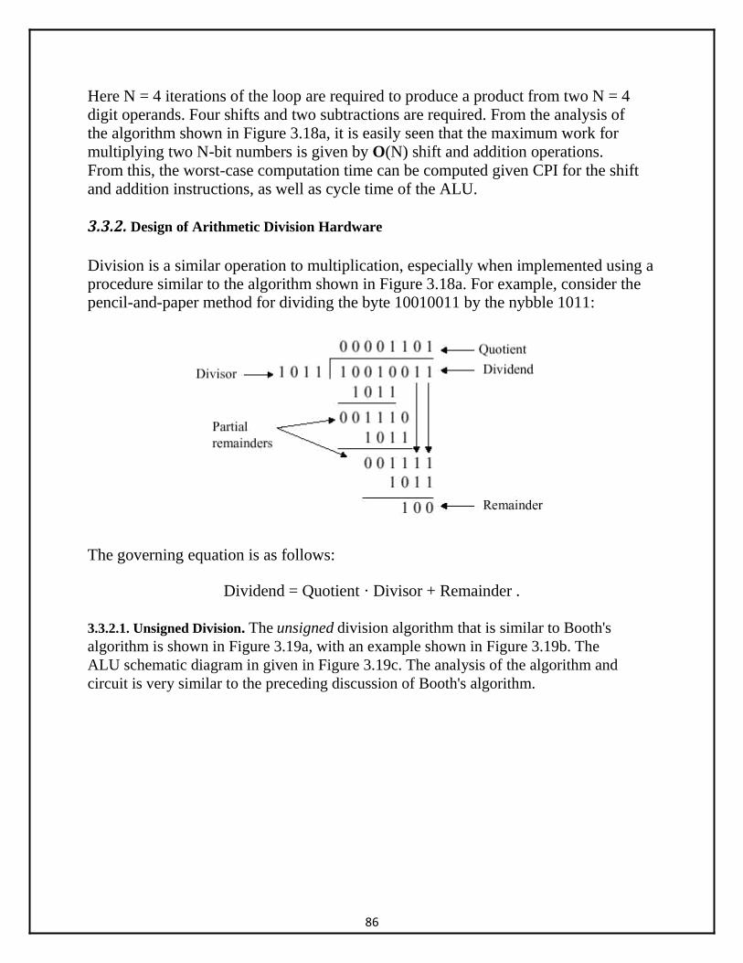
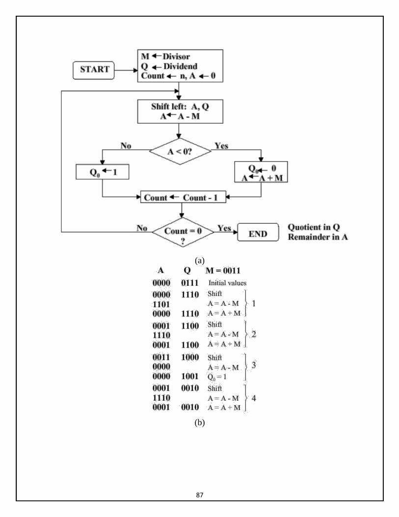
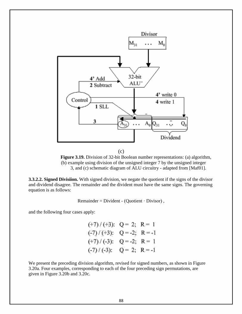
Unit-III CPU and Computer Arithmetic Classes: 11 CPU design: Instruction cycle, Data representation, Memory reference instructions, Input-Output, and Interrupt,
Addressing Modes, Data Transfer and Manipulation, Program Control. Computer Arithmetic: Addition and
Subtraction, Floating Point Arithmetic Operations, Decimal Arithmetic unit.
Unit-IV Input-Output Organization and Memory Organization Classes: 10 Memory organization: Memory hierarchy, Main Memory, Auxiliary Memory, Associative Memory, Cache
Memory, Virtual Memory. Input or Output Organization: Input or Output Interface, Asynchronous data transfer,
Modes of transfer, Priority Interrupt, Direct Memory Access.
Unit-V Multiprocessors Classes: 10
Pipeline: Parallel processing, Pipelining-Arithmetic pipeline, Instruction Pipeline. Multiprocessors: Characteristics of Multi Processors, Inter Connection Structures, Inter Processor Arbitration,
Inter Processor Communication and Synchronization. Text Books:
1. M. Morris Mano, “Computer Systems Architecture”, Pearson, 3rd Edition, 2007.
2. John D. Carpinelli, “Computer Systems Organization and Architecture”, Pearson, 1st Edition, 2001. 3. Patterson, Hennessy, “Computer Organization and Design: The Hardware/Software Interface”,
Morgan Kaufmann, 5th Edition, 2013. Reference Books:
1. John. P. Hayes, “Computer System Architecture”, McGraw Hill, 3rd Edition, 1998.
2. Carl Hamacher, Zvonko G Vranesic, Safwat G Zaky, “Computer Organization”, McGraw Hill,
5th Edition, 2002.
3. William Stallings, “Computer Organization and Architecture”, Pearson Edition, 8th Edition, 2010.
UNIT-1
INTRODUCTION TO COMPUTER ORGANIZATION
Basic Computer Organization – CPU Organization – Memory Subsystem Organization and Interfacing
– I/O Subsystem Organization and Interfacing – A Simple Computer- Levels of Programming
Languages, Assembly Language Instructions, Instruction Set Architecture Design, A simple Instruction
Set Architecture.
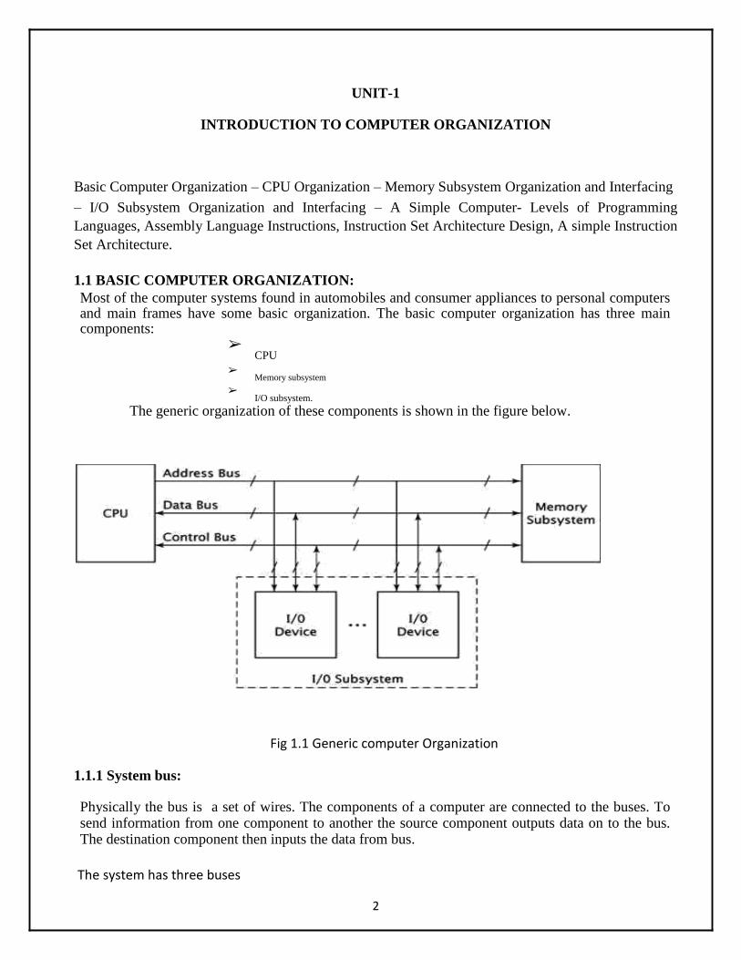
1.1 BASIC COMPUTER ORGANIZATION: Most of the computer systems found in automobiles and consumer appliances to personal computers and main frames have some basic organization. The basic computer organization has three main components:
➢ CPU
➢ Memory subsystem
➢ I/O subsystem.
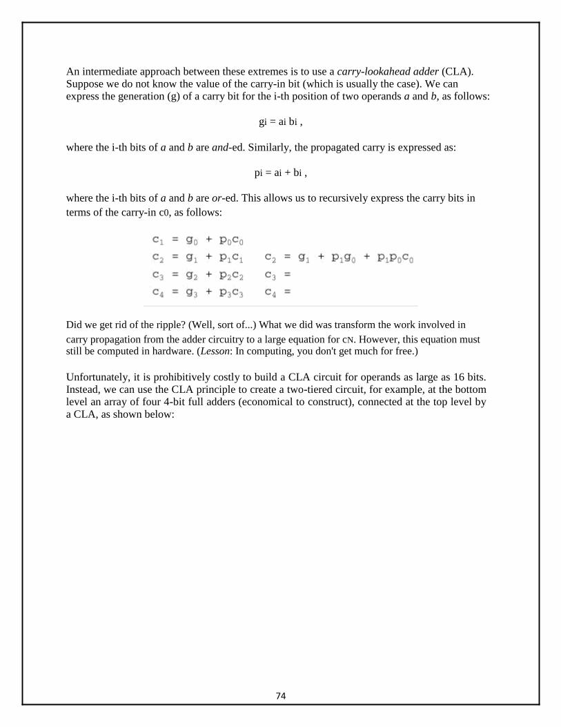
The generic organization of these components is shown in the figure below.
Fig 1.1 Generic computer Organization
1.1.1 System bus:
Physically the bus is a set of wires. The components of a computer are connected to the buses. To send information from one component to another the source component outputs data on to the bus. The destination component then inputs the data from bus.
The system has three buses
2
➢ Address bus
➢ Data bus
➢ Control bus
• The uppermost bus in this figure is the address bus. When the CPU reads data or instructions from or writes data to memory, it must specify the address of the memory location it wishes to access.
• Data is transferred via the data bus. When CPU fetches data from memory it first outputs the memory address on to its address bus. Then memory outputs the data onto the data bus. Memory then reads and stores the data at the proper locations.
• Control bus carries the control signal. Control signal is the collection of individual control signals. These signals indicate whether data is to be read into or written out of the CPU.
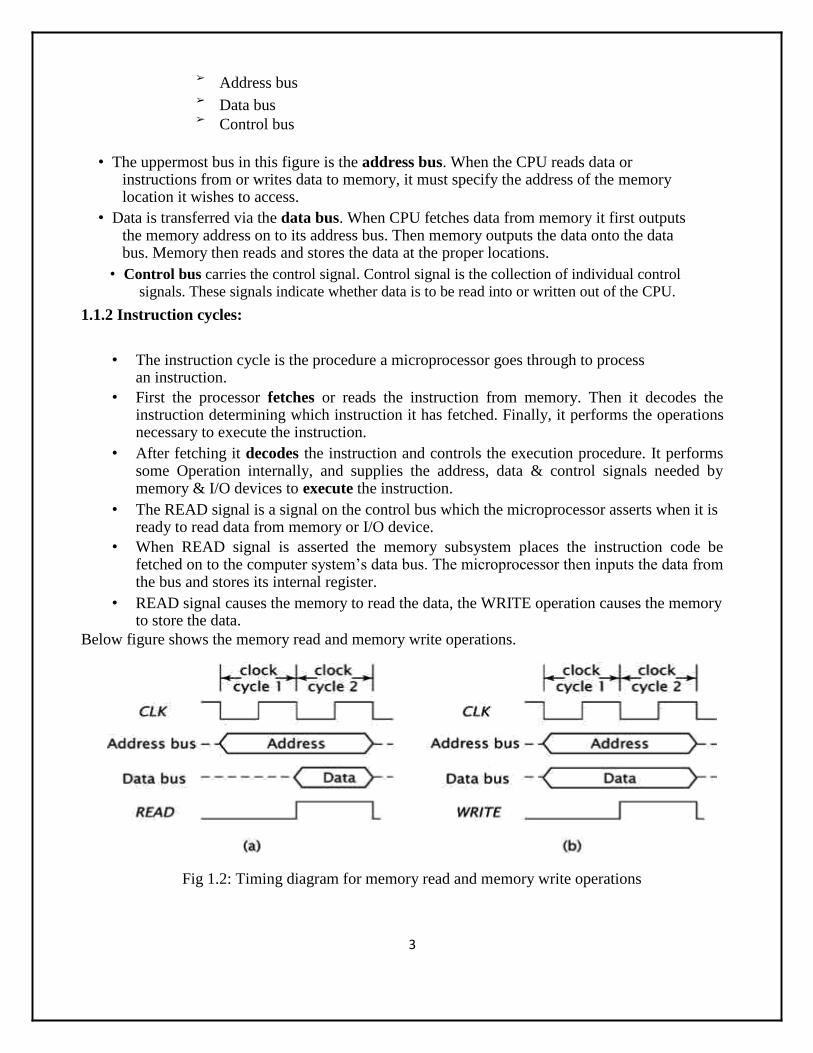
1.1.2 Instruction cycles:
• The instruction cycle is the procedure a microprocessor goes through to process an instruction.
• First the processor fetches or reads the instruction from memory. Then it decodes the instruction determining which instruction it has fetched. Finally, it performs the operations necessary to execute the instruction.
• After fetching it decodes the instruction and controls the execution procedure. It performs some Operation internally, and supplies the address, data & control signals needed by memory & I/O devices to execute the instruction.
• The READ signal is a signal on the control bus which the microprocessor asserts when it is ready to read data from memory or I/O device.
• When READ signal is asserted the memory subsystem places the instruction code be fetched on to the computer system’s data bus. The microprocessor then inputs the data from the bus and stores its internal register.
• READ signal causes the memory to read the data, the WRITE operation causes the memory to store the data.
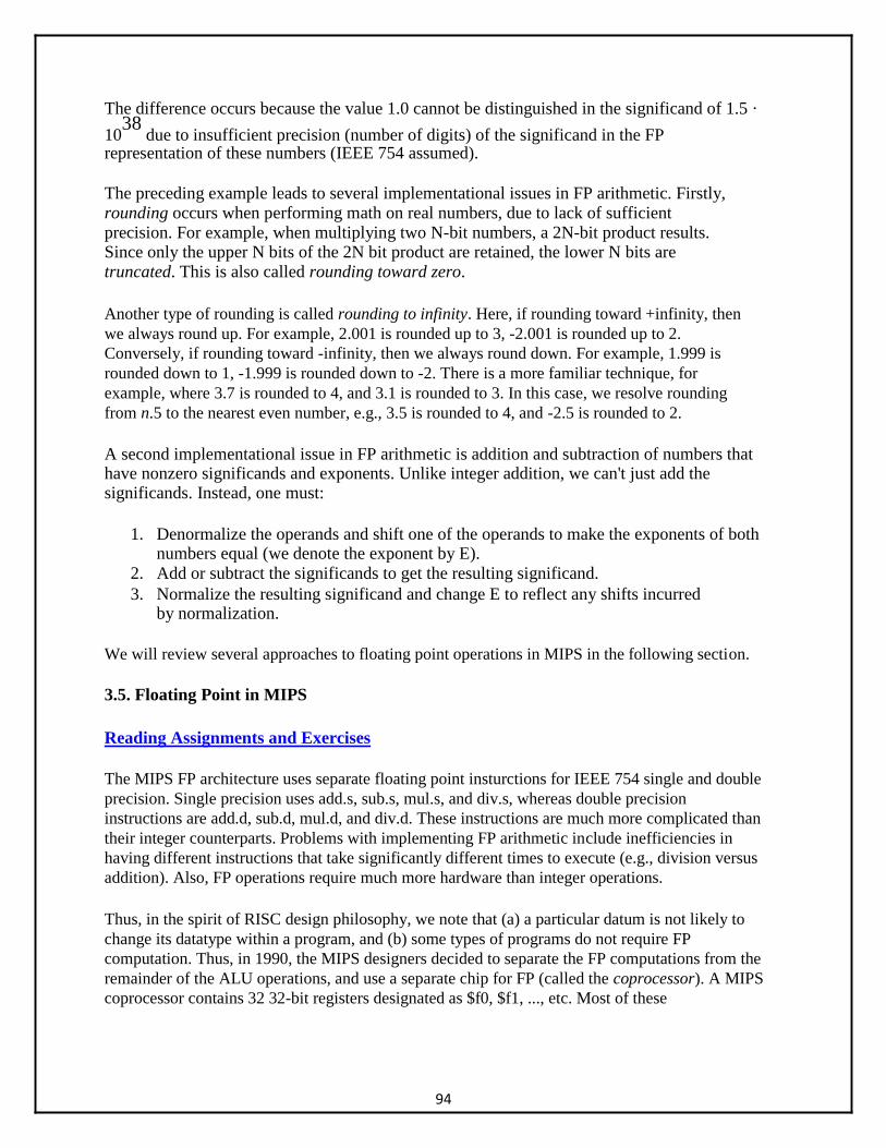
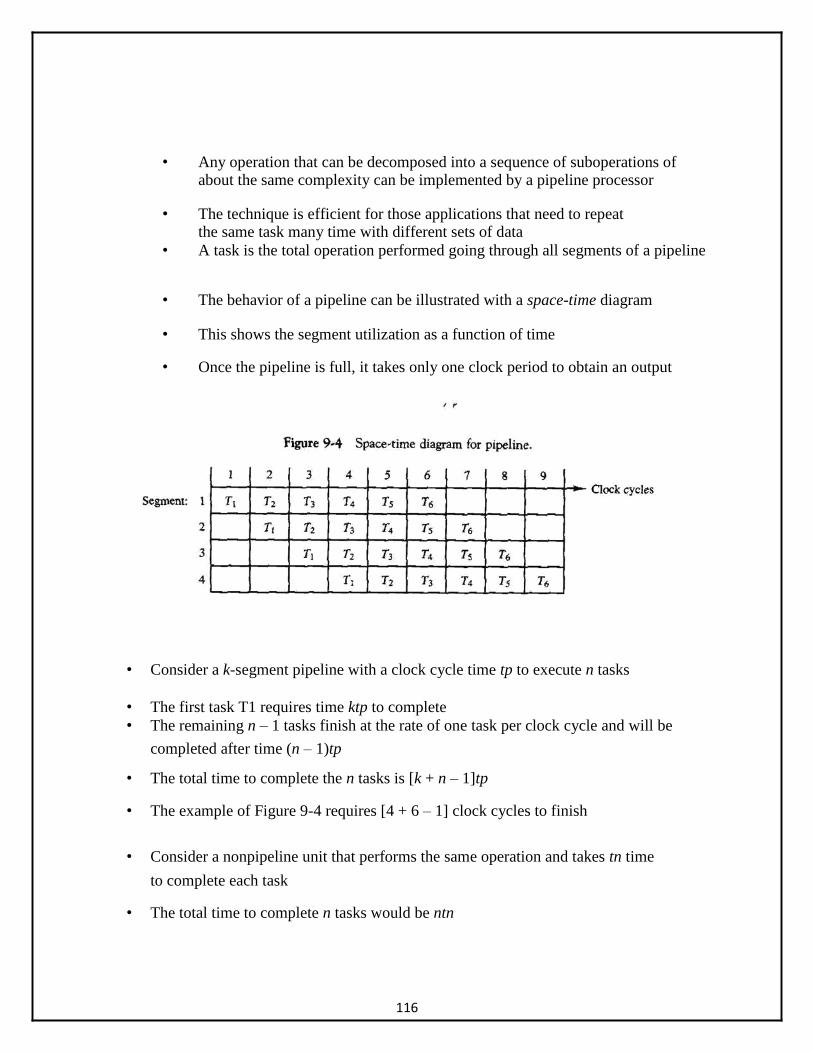
Below figure shows the memory read and memory write operations.
Fig 1.2: Timing diagram for memory read and memory write operations
3
• In the above figure the top symbol is CLK. This is the computer system clock. The
processor uses the system clock to synchronize its operations.
• In fig (a) the microprocessor places the address on to the bus at the beginning of a clock cycle, a
0/1 sequence of clock. One clock cycle later, to allow for memory to decode the address and access its
data, the microprocessor asserts the READ control signal. This causes the memory to place its data
onto the system data bus. During this clock cycle, the microprocessor reads the data off the system bus
and stores it in one of the registers. At the end of the clock cycle it removes the address from the
address bus and deasserts the READ signal. Memory then removes the data from the data from the data
bus completing the memory read operation.
• In fig(b) the processor places the address and data onto the system bus during the first clock
pulse. The microprocessor then asserts the WRITE control signal at the end of the second clock cycle.
At the end of the second clock cycle the processor completes the memory write operation by removing
the address and data from the system bus and deasserting the WRITE signal.
• I/O read and write operations are similar to the memory read and write operations. Basically
the processor may use memory mapped I/O and isolated I/O.
• In memory mapped I/O it fallows the same sequence of operations to input data as to read from
or write data into memory.
In isolated I/O fallow same process but have a second control signal to distinguish between I/O and
memory accesses. For example in 8085 microprocessor has a control signal called IO/ . The processor
set IO/ to 1 for I/O read and write operations and 0 for memory read and write operations.
1.2 CPU ORGANIZATION:
Central processing unit (CPU) is the electronic circuitry within a computer that carries out the instructions of a computer program by performing the basic arithmetic, logical, control and input/output (I/O) operations specified by the instructions.
In the computer all the all the major components are connected with the help of the system bus.
Data bus is used to shuffle data between the various components in a computer system.
To differentiate memory locations and I/O devices the system designer assigns a unique memory
address to each memory element and I/O device. When the software wants to access some particular
memory location or I/O device it places the corresponding address on the address bus. Circuitry
associated with the memory or I/O device recognizes this address and instructs the memory or I/O
device to read the data from or place data on the data bus. Only the device whose address matches the
value on the address bus responds.
The control bus is an electric collection of signals that control how the processor communicates with
the rest of the system. The read and write control lines control the direction of data on the data bus.
4
When both contain logic one the CPU and memory-I/O are not communicating with one another. If
the read line is low (logic zero) the CPU is reading data from memory (that is the system is
transferring data from memory to the CPU). If the write line is low the system transfers data from the
CPU to memory.
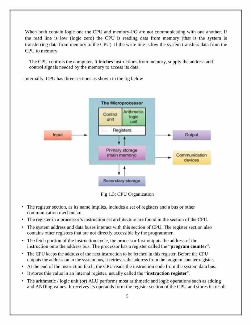
The CPU controls the computer. It fetches instructions from memory, supply the address and control signals needed by the memory to access its data.
Internally, CPU has three sections as shown in the fig below
Fig 1.3: CPU Organization
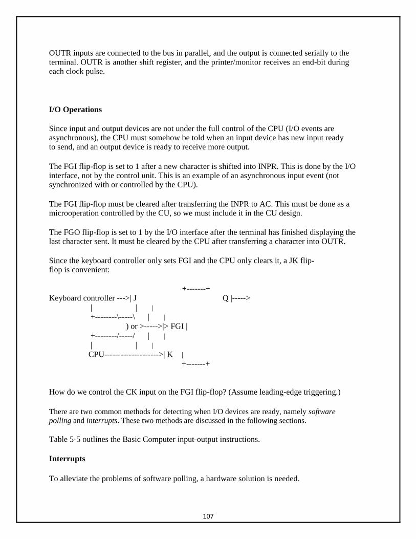
• The register section, as its name implies, includes a set of registers and a bus or other
communication mechanism. • The register in a processor’s instruction set architecture are found in the section of the CPU. • The system address and data buses interact with this section of CPU. The register section also
contains other registers that are not directly accessible by the programmer. • The fetch portion of the instruction cycle, the processor first outputs the address of the
instruction onto the address bus. The processor has a register called the “program counter”. • The CPU keeps the address of the next instruction to be fetched in this register. Before the CPU
outputs the address on to the system bus, it retrieves the address from the program counter register. • At the end of the instruction fetch, the CPU reads the instruction code from the system data bus. • It stores this value in an internal register, usually called the “instruction register”. • The arithmetic / logic unit (or) ALU performs most arithmetic and logic operations such as adding
and ANDing values. It receives its operands form the register section of the CPU and stores its result
5
back in the register section.
• Just as CPU controls the computer, the control unit controls the CPU. The control unit receives some
data values from the register unit, which it used to generate the control signals. This code generates
the instruction codes & the values of some flag registers. • The control unit also generates the signals for the system control bus such as READ, WRITE, IO/
signals.
1.3 MEMORY SUBSYSTEM ORGANIZATION AND INTERFACING:
Memory is the group of circuits used to store data. Memory components have some number of
memory locations, each word of which stores a binary value of some fixed length. The number of
locations and the size of each location vary from memory chip to memory chip, but they are fixed
within individual chip.
The size of the memory chip is denoted as the number of locations times the number of bits in each
location. For example, a memory chip of size 512×8 has 512 memory locations, each of which has
eight bits.The address inputs of a memory chip choose one of its locations. A memory chip with
2nlocations requires n address inputs.
• View the memory unit as a black box. Data transfer between the memory and the processor
takes place through the use of two registers called MAR (Memory Address Register) and
MDR (Memory data register).
• MAR is n-bits long and MDR is m-bits long, and data is transferred between the memory and
the processor. This transfer takes place over the processor bus.
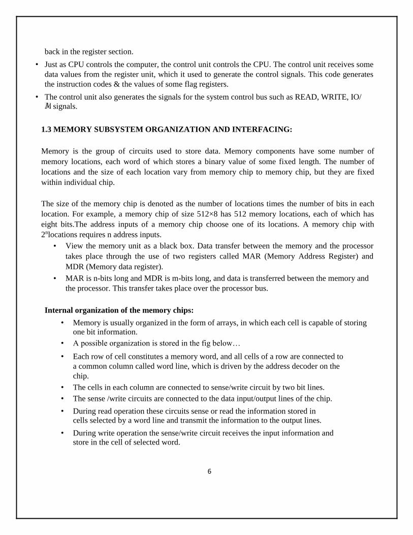
Internal organization of the memory chips:
• Memory is usually organized in the form of arrays, in which each cell is capable of storing one bit information.
• A possible organization is stored in the fig below…
• Each row of cell constitutes a memory word, and all cells of a row are connected to
a common column called word line, which is driven by the address decoder on the
chip. • The cells in each column are connected to sense/write circuit by two bit lines. • The sense /write circuits are connected to the data input/output lines of the chip.
• During read operation these circuits sense or read the information stored in
cells selected by a word line and transmit the information to the output lines.
• During write operation the sense/write circuit receives the input information and store in the cell of selected word.
6
Types of Memory: There are two types of memory chips 1. Read Only Memory (ROM)
2. Random Access Memory (RAM)
a) ROM Chips:
ROM chips are designed for applications in which data is read. These chips are
programmed with data by an external programming unit before they are added to the
computer system. Once it is done the data does not change. A ROM chip always retains its
data, even when
Power to chip is turned off so ROM is called nonvolatile because of its property. There are
several types of ROM chips which are differentiated by how often they are programmed.
➢ Masked ROM(or) simply ROM
➢ PROM(Programmed Read Only Memory)
➢ EPROM(Electrically Programmed Read Only Memory)
➢ EEPROM(Electrically Erasable PROM)
➢ Flash Memory
• A masked ROM or simply ROM is programmed with data as chip is fabricated.
• The mask is used to create the chip and chip is designed with the required data hardwired in it.
Once chip is designed the data will not change. Figure below shows the possible configuration of
the ROM cell.
• Logic 0 is stored in the cell if the transistor is connected to ground at point P, other wise
1 stored.
• A sense circuit at the end of the bit line generates at the high voltage indicating a 1.Data are written into the ROM when it is manufactured.
PROM
• Some ROM designs allow the data to be loaded by the user, thus providing programmable ROM (PROM).
• Programmability is achieved by inserting a fuse at point P in the above fig. Before it
is programmed, the memory contains all 0’s.
• The user insert 1’s at the required locations by burning out the fuse at these locations using high current pulse.
• The fuses in PROM cannot restore once they are blown, PROM’s can only be
programmed once.
2) EPROM
• EPROM is the another ROM chip allows the stored data to be erased and new data to be loaded. Such an erasable reprogrammable ROM is usually called an EPROM.
7
• Programming in EPROM is done by charging of capacitors. The charged and
uncharged capacitors cause each word of memory to store the correct value.
• The chip is erased by being placed under UV light, which causes the capacitor to leak their charge.
3) EEPROM
• A significant disadvantage of the EPROM is the chip is physically removed from the circuit for reprogramming and that entire contents are erased by the UV light.
• Another version of EPROM is EEPROM that can be both programmed and erased
electrically, such chips called EEPROM, do not have to remove for erasure.
• The only disadvantage of EEPROM is that different voltages are need for erasing, writing, reading and stored data.
4) Flash Memory
• A special type of EEPROM is called a flash memory is electrically erase data in blocks rather than individual locations.
• It is well suited for the applications that writes blocks of data and can be used as a solid
state hard disk. It is also used for data storage in digital computers.
RAM Chips:
• RAM stands for Random access memory. This often referred to as read/write memory. Unlike the ROM it initially contains no data.
• The digital circuit in which it is used stores data at various locations in the RAM
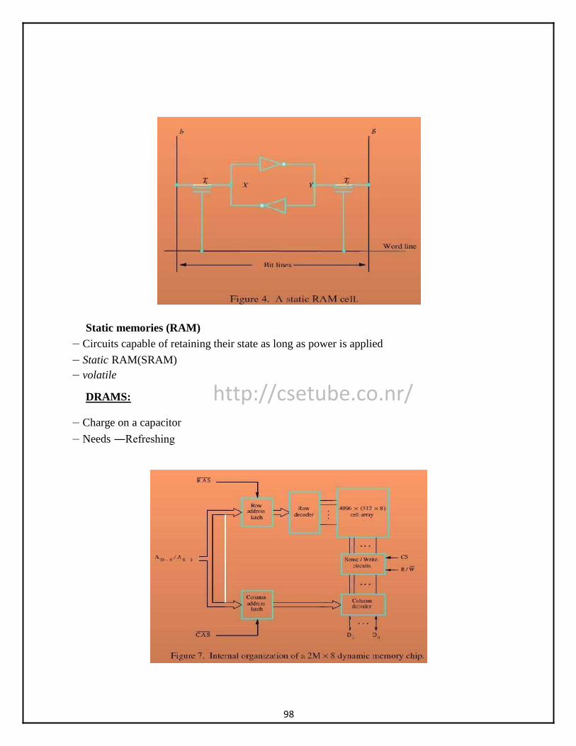
are retrieves data from these locations. • The data pins are bidirectional unlike in ROM. • A ROM chip loses its data once power is removed so it is a volatile memory. • RAM chips are differentiated based on the data they maintain.
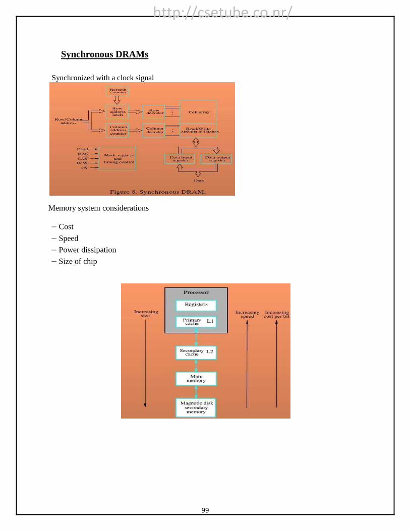
➢ Dynamic RAM (DRAM)
➢ Static RAM (SRAM)
1. Dynamic RAM:
• DRAM chips are like leaky capacitors. Initially data is stored in the DRAM chip, charging its memory cells to their maximum values.
• The charging slowly leaks out and would eventually go too low to represent valid data.
• Before this a refresher circuit reads the content of the DRAM and rewrites data to its original locations.
• DRAM is used to construct the RAM in personal computers. • DRAM memory cell is shown in the figure below.
8
2. Static RAM: • Static RAM are more likely the register .Once the data is written to SRAM, its contents stay valid it does not have to be refreshed. • Static RAM is faster than DRAM but it is also much more expensive. Cache memory in the personal computer is constructed from SRAM. ➢ Various factors such as cost, speed, power consumption and size of the chip determine how a RAM is chosen for a given application
➢ Static RAMs:
o Chosen when speed is the primary concern. o Circuit implementing the basic cell is highly complex, so cost and size
are affected. o Used mostly in cache memories.
➢ Dynamic RAMs:
o Predominantly used for implementing computer main memories. o High densities available in these chips. o Economically viable for implementing large memories
Memory subsystem configuration:
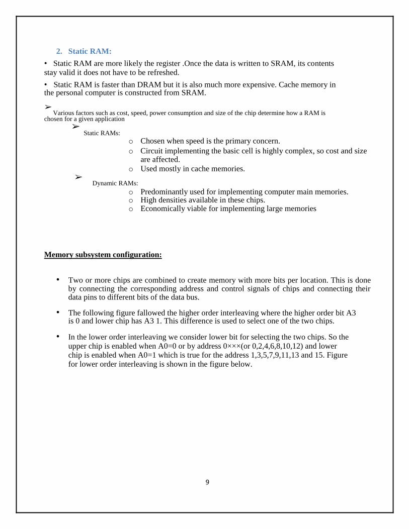
• Two or more chips are combined to create memory with more bits per location. This is done by connecting the corresponding address and control signals of chips and connecting their data pins to different bits of the data bus.
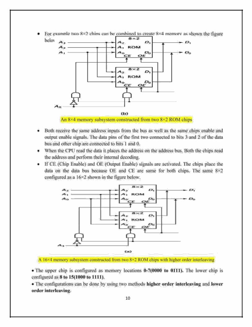
• The following figure fallowed the higher order interleaving where the higher order bit A3
is 0 and lower chip has A3 1. This difference is used to select one of the two chips.
• In the lower order interleaving we consider lower bit for selecting the two chips. So the upper chip is enabled when A0=0 or by address 0×××(or 0,2,4,6,8,10,12) and lower chip is enabled when A0=1 which is true for the address 1,3,5,7,9,11,13 and 15. Figure for lower order interleaving is shown in the figure below.
9
10
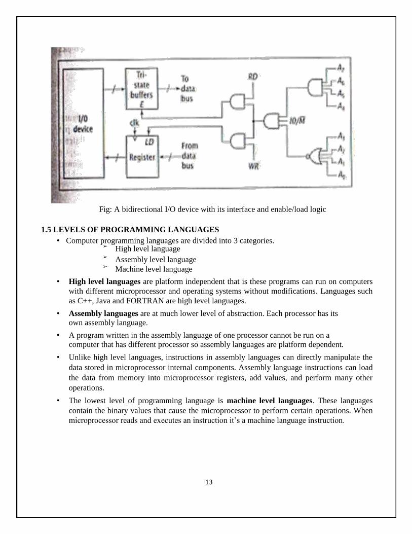
1.4 I/O SUBSYSTEM ORGANIZATION AND INTERFACING
The I/O subsystem is treated as an independent unit in the computer The CPU initiates I/O commands generically
➢ Read, write, scan, etc.
Below figure shows the basic connection between the CPU, memory to the I/O device .The I/O
device is connected to the computer system address, data and control buses. Each I/O device
includes I/O circuitry that interacts with the buses.
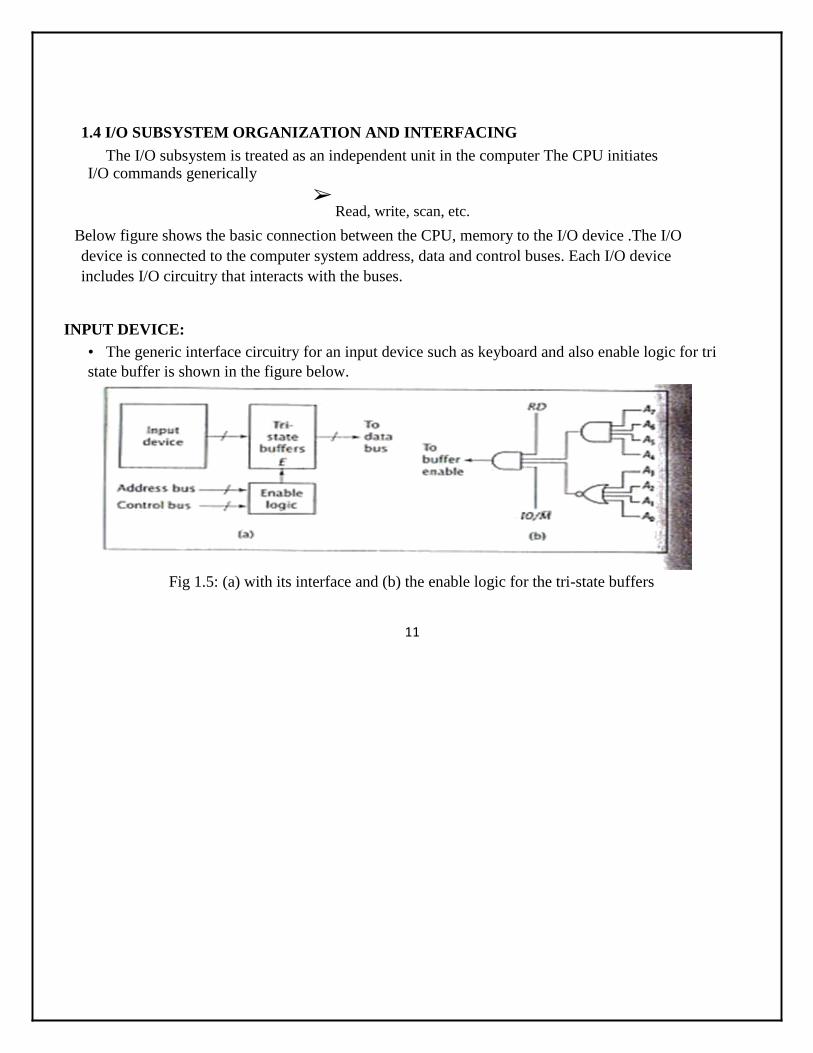
INPUT DEVICE:
• The generic interface circuitry for an input device such as keyboard and also enable logic for tri
state buffer is shown in the figure below.
Fig 1.5: (a) with its interface and (b) the enable logic for the tri-state buffers
11
• The data from the input device goes to the tri-state buffers. When the value in the address and control
buses are correct, the buffers are enabled and data passes on the data bus. • The CPU can then read this data. If the conditions are not right the logic block does not enable
the buffers and do not place on the bus. • The enable logic contains 8-bit address and also generates two control signals RD and IO/ .
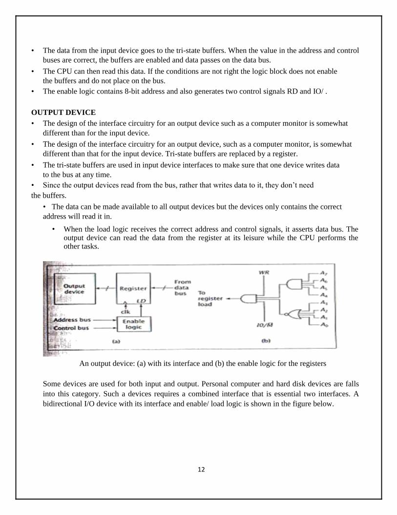
OUTPUT DEVICE
• The design of the interface circuitry for an output device such as a computer monitor is somewhat
different than for the input device. • The design of the interface circuitry for an output device, such as a computer monitor, is somewhat
different than that for the input device. Tri-state buffers are replaced by a register. • The tri-state buffers are used in input device interfaces to make sure that one device writes data
to the bus at any time. • Since the output devices read from the bus, rather that writes data to it, they don’t need the buffers.
• The data can be made available to all output devices but the devices only contains the correct
address will read it in.
• When the load logic receives the correct address and control signals, it asserts data bus. The output device can read the data from the register at its leisure while the CPU performs the other tasks.
An output device: (a) with its interface and (b) the enable logic for the registers
Some devices are used for both input and output. Personal computer and hard disk devices are falls
into this category. Such a devices requires a combined interface that is essential two interfaces. A
bidirectional I/O device with its interface and enable/ load logic is shown in the figure below.
12
Fig: A bidirectional I/O device with its interface and enable/load logic
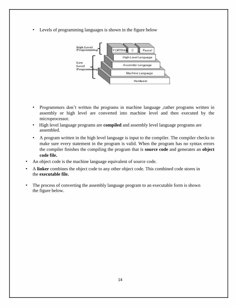
1.5 LEVELS OF PROGRAMMING LANGUAGES
• Computer programming languages are divided into 3 categories. ➢ High level language
➢ Assembly level language
➢ Machine level language
• High level languages are platform independent that is these programs can run on computers
with different microprocessor and operating systems without modifications. Languages such
as C++, Java and FORTRAN are high level languages.
• Assembly languages are at much lower level of abstraction. Each processor has its own assembly language.
• A program written in the assembly language of one processor cannot be run on a
computer that has different processor so assembly languages are platform dependent.
• Unlike high level languages, instructions in assembly languages can directly manipulate the
data stored in microprocessor internal components. Assembly language instructions can load
the data from memory into microprocessor registers, add values, and perform many other
operations.
• The lowest level of programming language is machine level languages. These languages
contain the binary values that cause the microprocessor to perform certain operations. When
microprocessor reads and executes an instruction it’s a machine language instruction.
13
• Levels of programming languages is shown in the figure below
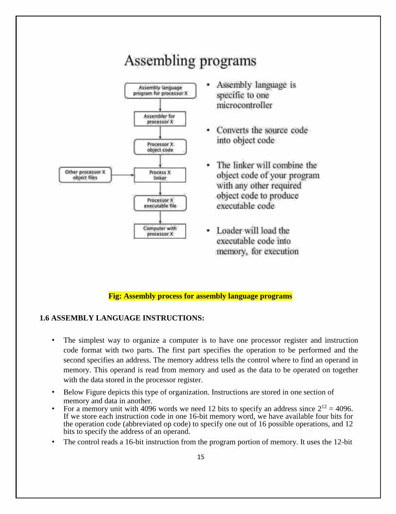
• Programmers don’t written the programs in machine language ,rather programs written in
assembly or high level are converted into machine level and then executed by the
microprocessor. • High level language programs are compiled and assembly level language programs are
assembled.
• A program written in the high level language is input to the compiler. The compiler checks to
make sure every statement in the program is valid. When the program has no syntax errors
the compiler finishes the compiling the program that is source code and generates an object
code file. • An object code is the machine language equivalent of source code. • A linker combines the object code to any other object code. This combined code stores in
the executable file.
• The process of converting the assembly language program to an executable form is shown
the figure below.
14
Fig: Assembly process for assembly language programs
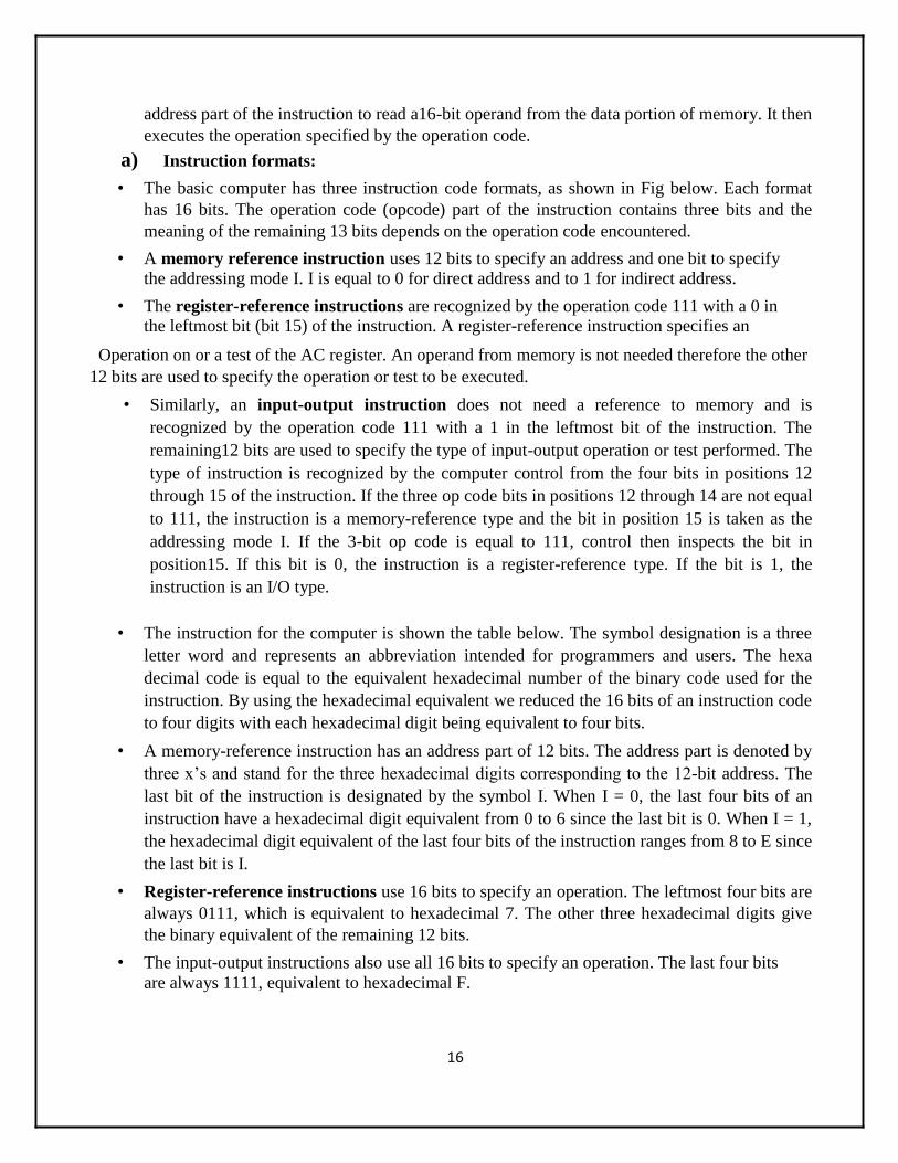
1.6 ASSEMBLY LANGUAGE INSTRUCTIONS:
• The simplest way to organize a computer is to have one processor register and instruction
code format with two parts. The first part specifies the operation to be performed and the
second specifies an address. The memory address tells the control where to find an operand in
memory. This operand is read from memory and used as the data to be operated on together
with the data stored in the processor register.
• Below Figure depicts this type of organization. Instructions are stored in one section of memory and data in another.
• For a memory unit with 4096 words we need 12 bits to specify an address since 212 = 4096. If we store each instruction code in one 16-bit memory word, we have available four bits for the operation code (abbreviated op code) to specify one out of 16 possible operations, and 12 bits to specify the address of an operand.
• The control reads a 16-bit instruction from the program portion of memory. It uses the 12-bit
15
address part of the instruction to read a16-bit operand from the data portion of memory. It then
executes the operation specified by the operation code.
a) Instruction formats:
• The basic computer has three instruction code formats, as shown in Fig below. Each format
has 16 bits. The operation code (opcode) part of the instruction contains three bits and the
meaning of the remaining 13 bits depends on the operation code encountered.
• A memory reference instruction uses 12 bits to specify an address and one bit to specify the addressing mode I. I is equal to 0 for direct address and to 1 for indirect address.
• The register-reference instructions are recognized by the operation code 111 with a 0 in
the leftmost bit (bit 15) of the instruction. A register-reference instruction specifies an
Operation on or a test of the AC register. An operand from memory is not needed therefore the other
12 bits are used to specify the operation or test to be executed.
• Similarly, an input-output instruction does not need a reference to memory and is
recognized by the operation code 111 with a 1 in the leftmost bit of the instruction. The
remaining12 bits are used to specify the type of input-output operation or test performed. The
type of instruction is recognized by the computer control from the four bits in positions 12
through 15 of the instruction. If the three op code bits in positions 12 through 14 are not equal
to 111, the instruction is a memory-reference type and the bit in position 15 is taken as the
addressing mode I. If the 3-bit op code is equal to 111, control then inspects the bit in
position15. If this bit is 0, the instruction is a register-reference type. If the bit is 1, the
instruction is an I/O type.
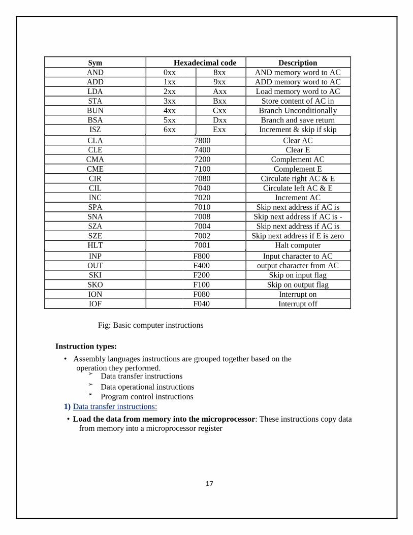
• The instruction for the computer is shown the table below. The symbol designation is a three
letter word and represents an abbreviation intended for programmers and users. The hexa
decimal code is equal to the equivalent hexadecimal number of the binary code used for the
instruction. By using the hexadecimal equivalent we reduced the 16 bits of an instruction code
to four digits with each hexadecimal digit being equivalent to four bits.
• A memory-reference instruction has an address part of 12 bits. The address part is denoted by
three x’s and stand for the three hexadecimal digits corresponding to the 12-bit address. The
last bit of the instruction is designated by the symbol I. When I = 0, the last four bits of an
instruction have a hexadecimal digit equivalent from 0 to 6 since the last bit is 0. When I = 1,
the hexadecimal digit equivalent of the last four bits of the instruction ranges from 8 to E since
the last bit is I.
• Register-reference instructions use 16 bits to specify an operation. The leftmost four bits are
always 0111, which is equivalent to hexadecimal 7. The other three hexadecimal digits give
the binary equivalent of the remaining 12 bits.
• The input-output instructions also use all 16 bits to specify an operation. The last four bits
are always 1111, equivalent to hexadecimal F.
16
Sym Hexadecimal code Description
AND 0xx 8xx AND memory word to AC
ADD 1xx 9xx ADD memory word to AC
LDA 2xx Axx Load memory word to AC
STA 3xx Bxx Store content of AC in
BUN 4xx Cxx Branch Unconditionally
BSA 5xx Dxx Branch and save return
ISZ 6xx Exx Increment & skip if skip
CLA 7800 Clear AC
CLE 7400 Clear E
CMA 7200 Complement AC
CME 7100 Complement E
CIR 7080 Circulate right AC & E
CIL 7040 Circulate left AC & E
INC 7020 Increment AC
SPA 7010 Skip next address if AC is
SNA 7008 Skip next address if AC is -
SZA 7004 Skip next address if AC is
SZE 7002 Skip next address if E is zero
HLT 7001 Halt computer
INP F800 Input character to AC
OUT F400 output character from AC
SKI F200 Skip on input flag
SKO F100 Skip on output flag
ION F080 Interrupt on
IOF F040 Interrupt off
Fig: Basic computer instructions
Instruction types:
• Assembly languages instructions are grouped together based on the operation they performed.
➢ Data transfer instructions
➢ Data operational instructions
➢ Program control instructions
1) Data transfer instructions:
• Load the data from memory into the microprocessor: These instructions copy data
from memory into a microprocessor register
17
• Store the data from the microprocessor into the memory: This is similar to the load
data expect data is copied in the opposite direction from a microprocessor register to
memory.
• Move data within the microprocessor: These operations copies data from one
microprocessor register to another.
• Input the data to the microprocessor: The microprocessor inputs the data from the input devices ex: keyboard in to one of its registers.
• Output the data from the microprocessor: The microprocessor copies the data from
one of the registers to an input device such as digital display of a microwave oven.
2) Data operational instructions:
• Data operational instructions do modify their data values. They typically perform some operations using one or two data values (operands) and store result.
• Arithmetic instructions make up a large part of data operations instructions.
Instructions that add, subtract, multiply, or divide values fall into this category. An
instruction that increment or decrement also falls in to this category.
• Logical instructions perform basic logical operations on data. They AND, OR, or XOR two data values or complement a single value.
• Shift operations as their name implies shift the bits of a data values also comes
under this category. 3) Program control instructions:
• Program control instructions are used to control the flow of a program. Assembly
language instructions may include subroutines like in high level language
program may have subroutines, procedures, and functions.
• A jump or branch instructions are generally used to go to another part of the program or subroutine.
• A microprocessor can be designed to accept interrupts. An interrupt causes the
processor to stop what is doing and start other instructions. Interrupts may be software
or hardware.
• One final type of control instructions is halt instruction. This instruction causes a processor to stop executing instructions such as end of a program.
1.7 Instruction set architecture(ISA) design:
• Designing of the instruction set is the most important in designing the microprocessor. A poor designed ISA even it is implemented well leads to bad micro processor.
• A well designed instruction set architecture on the other hand can result in a
powerful processor that can meet variety of needs.
• In designing ISA the designer must evaluate the tradeoffs in performance and such constrains issues as size and cost when designing ISA specifications.
• If the processor is to be used for general purpose computing such as personal computer it will probably require a rich set of ISA. It will need a relatively large instruction set to
18
perform the wide variety of tasks it must accomplish. It may also need
many registers for some of these tasks.
• In contrast consider a microwave oven it require only simple ISA those need to control
the oven. This issue of completeness of the ISA is one of the criteria in designing the
processor that means the processor must have complete set of instructions to perform
the task of the given application.
• Another criterion is instruction orthogonality. Instructions are orthogonal if they do not
overlap, or perform the same function. A good instruction set minimizes the overlap
between instructions.
• Another area that the designer can optimize the ISA is the register set. Registers have a
large effect on the performance of a CPU. The CPU Can store data in its internal
registers instead of memory. The CPU can retrieve data from its registers much more
likely than form the memory.
• Having too few registers causes a program to make more reference to the memory thus reducing performance.
General purposes CPU have many registers since they have to process different types of
programs. Intel processor has 128 general purpose registers for integer data and another 128 for
floating point data. For dedicated CPU such as microwave oven having too many registers adds
unnecessary hardware to the CPU without providing any benefits.
1.7 A RELATIVELY SIMPLE INSTRUCTION SET ARCHITECTURE:
• A relatively simple instruction set architecture describes the ISA of the simple processor or CPU.
• A simple microprocessor can access 64K (=216) bytes of memory with each byte having 8 bits or 64K×8 of memory. This does not mean that every computer constructed using this relatively simple CPU must have full 64K of memory. A system based on this processor can have less than memory if doesn’t need the maximum 64K of memory.
• This processor inputting the data from and outputting the data to external devices such
as microwave ovens keypad and display are treated as memory accesses. There are
two types of input/output interactions that can design a CPU to perform. ➢ Isolated I/O
➢ Memory mapped I/O
• An isolated I/O input and output devices are treated as being separated from memory. Different instructions are used for memory and I/O.
• Memory mapped I/O treats input and output devices as memory locations the CPU
access these I/O devices using the same instructions that it uses to access memory. For
relatively simple CPU memory mapped I/O is used. • There are three registers in ISA of this processor.
➢ Accumulator (AC)
19
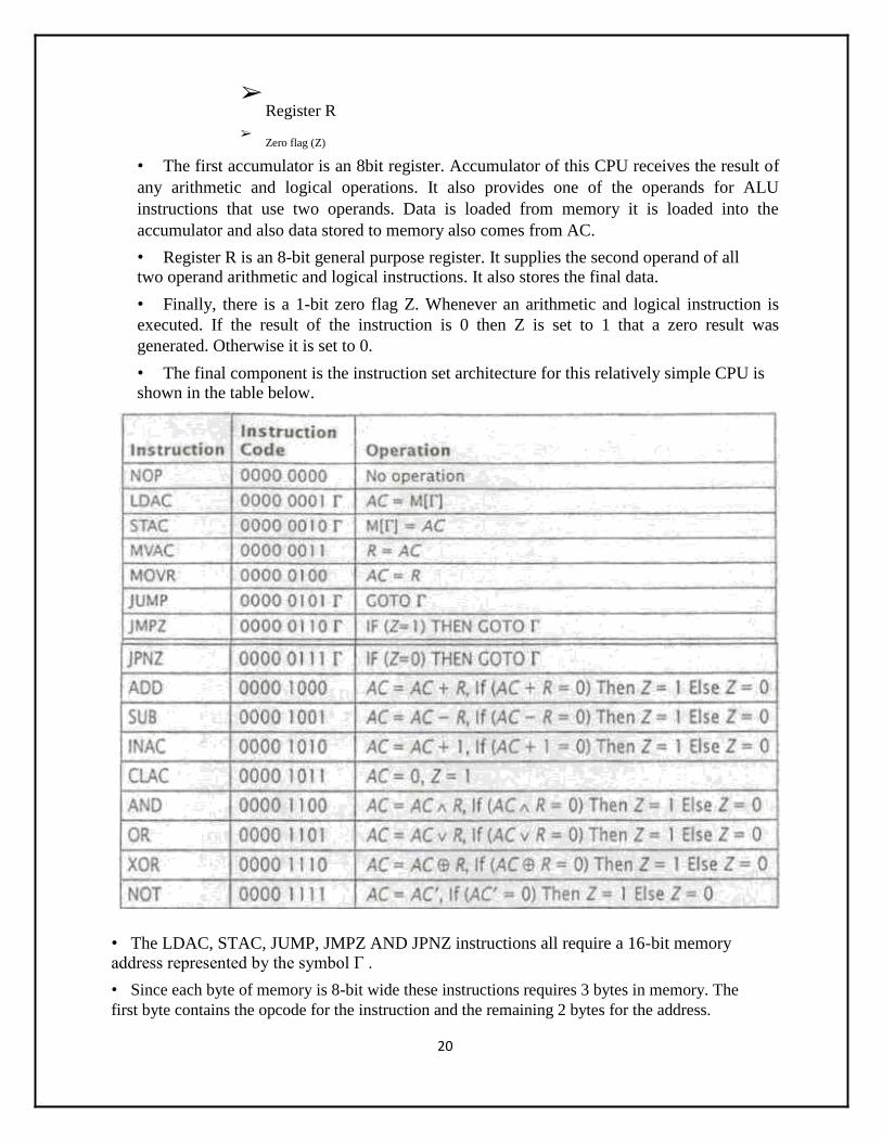
➢ Register R
➢ Zero flag (Z)
• The first accumulator is an 8bit register. Accumulator of this CPU receives the result of
any arithmetic and logical operations. It also provides one of the operands for ALU
instructions that use two operands. Data is loaded from memory it is loaded into the
accumulator and also data stored to memory also comes from AC.
• Register R is an 8-bit general purpose register. It supplies the second operand of all two operand arithmetic and logical instructions. It also stores the final data.
• Finally, there is a 1-bit zero flag Z. Whenever an arithmetic and logical instruction is
executed. If the result of the instruction is 0 then Z is set to 1 that a zero result was
generated. Otherwise it is set to 0.
• The final component is the instruction set architecture for this relatively simple CPU is shown in the table below.
• The LDAC, STAC, JUMP, JMPZ AND JPNZ instructions all require a 16-bit memory address represented by the symbol Γ .
• Since each byte of memory is 8-bit wide these instructions requires 3 bytes in memory. The
first byte contains the opcode for the instruction and the remaining 2 bytes for the address.
20
• The instructions of this instruction set architecture can be grouped in to 3 categories ➢ Data transfer instructions
➢ Program control instructions
➢ Data operational instructions
• The NOP, LDAC, STAC, MVAC or MOVR instructions are data transfer instructions.
The NOP operation performs no operation. The LDAC operation loads the data from the
memory it reads the data from the memory location M[Γ]. The STAC performs opposite,
copying data from AC to the memory location Γ.
• The MOVAC instruction copies data from R to AC and MOVR instruction copies the data from R to AC.
• There are three program control instructions in the instruction set: JUMP, JUPZ and JPNZ. The JUMP is the unconditional it always jumps to the memory location Γ. For example
JUMP 1234H instruction always jump to the memory location 1234H. The JUMP instruction
uses the immediate addressing mode since the jump address is specified in the instruction. The other two program control instructions JUPZ and JPNZ are conditional. If their conditions are
met Z=0 for JUPZ and Z=1 for JPNZ these instructions jump to the memory locationΓ.
• Finally data operations instructions are ADD, SUB, INAC and CLAC instructions are
arithmetic instructions. The ADD instructions add the content of AC and R and store the result
again in AC. The instruction also set the zero flag Z =1 if sum is zero or Z=0 if the sum is non
zero value. The SUB operation performs the same but it subtracts the AC and R.
• INAC instruction adds 1 to the AC and sets Z to its proper value. The CLAC instruction always makes Z=1 because it clears the AC value that is AC to 0.
• The last four data operation instructions are logical instructions as the name imply the AND,
OR, and XOR instructions logically AND,OR and XOR the values AC and R and store the
result in AC. The NOT instruction sets AC to its bitwise complement.
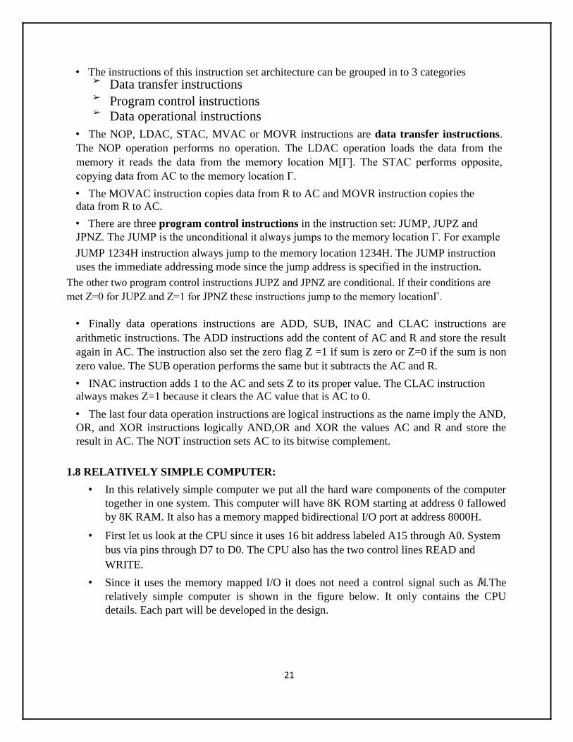
1.8 RELATIVELY SIMPLE COMPUTER:
• In this relatively simple computer we put all the hard ware components of the computer
together in one system. This computer will have 8K ROM starting at address 0 fallowed
by 8K RAM. It also has a memory mapped bidirectional I/O port at address 8000H.
• First let us look at the CPU since it uses 16 bit address labeled A15 through A0. System
bus via pins through D7 to D0. The CPU also has the two control lines READ and WRITE.
• Since it uses the memory mapped I/O it does not need a control signal such as .The
relatively simple computer is shown in the figure below. It only contains the CPU
details. Each part will be developed in the design.
21
Fig: A relatively simple computer: CPU details only
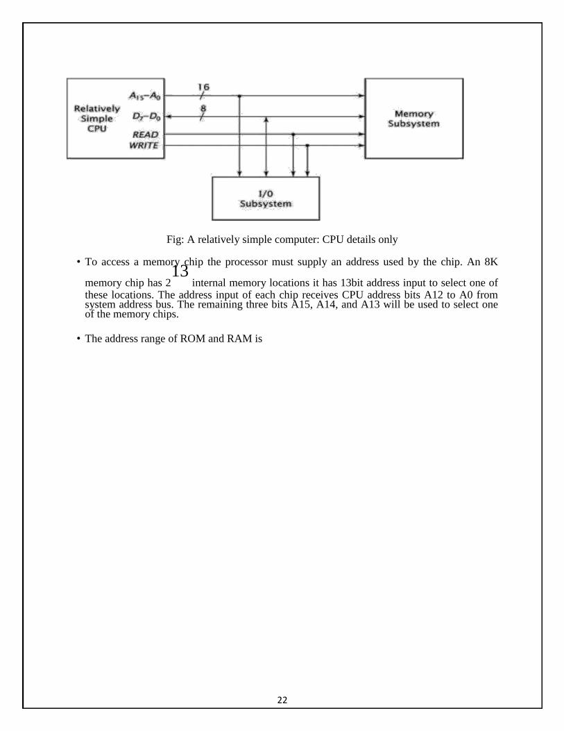
• To access a memory chip the processor must supply an address used by the chip. An 8K
memory chip has 213
internal memory locations it has 13bit address input to select one of these locations. The address input of each chip receives CPU address bits A12 to A0 from system address bus. The remaining three bits A15, A14, and A13 will be used to select one of the memory chips.
• The address range of ROM and RAM is
22
Unit-2
ORGANIZATION OF A COMPUTER
Register transfer: Register transfer language, register transfer, bus and memory transfers,
arithmetic micro operations, logic micro operations, And shift micro operations; Control unit:
Control memory, address sequencing, micro program example, and design of control unit.
Register Transfer and Microoperations
2.1 Register Transfer Language
• A digital system is an interconnection of digital hardware module.Digital systems varies in size and complexity from a few integrated circuits to a complex of interconnected and interacting digital computers.
• Digital system design invariably uses a modular approach. The modules are constructed from such digital components as registers, decoders, arithmetic elements, and control logic.
• The various modules are interconnected with common data and control paths to form a digital computer system.
• Digital modules are best defined by the registers they contain and the operations that are performed on the data stored in them. The operations executed on data stored in registers are called microoperations.
• A microoperation is an elementary operation performed on the information stored in one or more registers.
• The result of the operation may replace the previous binary information of a register or may be transferred to another register. Examples of microoperations are shift, count, clear, and load.
The internal hardware organization of a digital computer is best defined by specifying:
1. The set of registers it contains and their function.
2. The sequence of microoperations performed on the binary information stored in the registers.
3. The control that initiates the sequence of microoperations.
• The symbolic notation used to describe the microoperation transfers among registers is
called a register transfer language. • The term "register transfer" implies the availability of hardware logic circuits that can
perform a stated microoperation and transfer the result of the operation to the same or another register.
• The word "language" is borrowed from programmers, who apply this term to programming languages. A programming language is a procedure for writing symbols to specify a given computational process.
• A register transfer language is a system for expressing in symbolic form the microoperation sequences among the registers of a digital module.
• It is a convenient tool for describing the internal organization of digital computers in
23
concise and precise manner. It can also be used to facilitate the design process of digital systems.
• The register transfer language adopted here is believed to be as simple as possible, so
it should not take very long to memorize. • To define symbols for various types of microoperations, and at the same time,
describe associated hardware that can implement the stated microoperations. • Other symbology in use can easily be learned once this language has become familiar, for
most of the differences between register transfer languages consist of variations in detail rather than in overall purpose.
2.2 Register Transfer
• Computer registers are designated by capital letters (sometimes followed by numerals) to denote the function of the register. For example, MAR,PC,IR The individual flip-flops
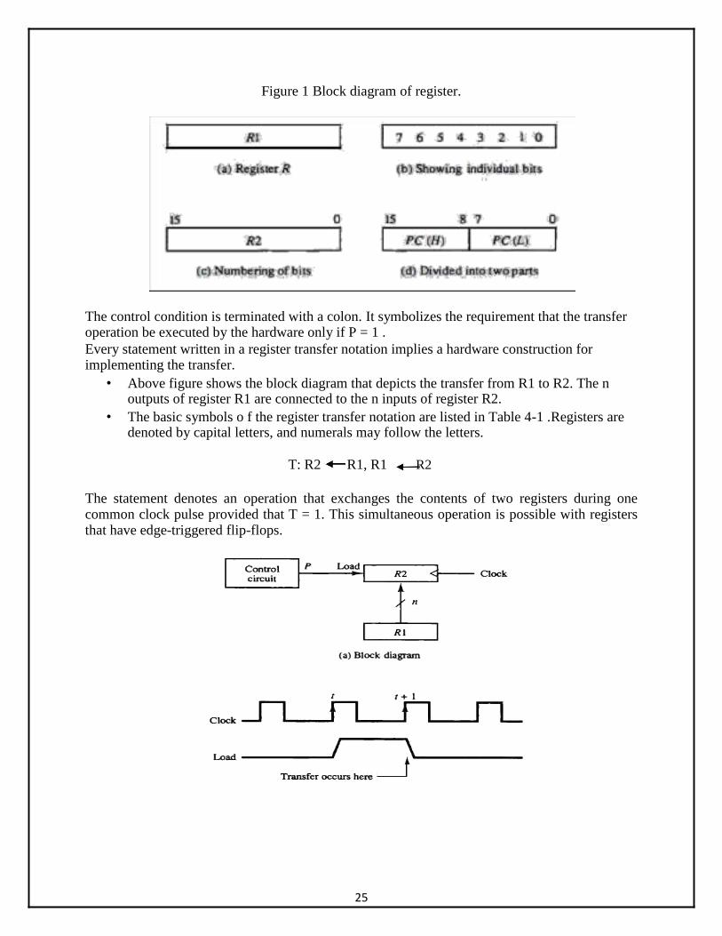
• Figure 1 shows the representation of registers in block diagram form. The most common
way to represent a register is by a rectangular box with the name of the register inside, as in Fig. 1(a) the individual bits can be distinguished as in (b). The numbering of bits in a 16-bit register can be marked on top of the box as shown in (c). A 16-bit register is partitioned into two parts in (d). Bits 0 through 7 are assigned the symbol L (for low byte) and bits 8 through 15 are assigned the symbol H (for high byte). The name of the 16-bit register is PC. The symbol PC (0-7) or PC(L) refers to the low-order byte and PC(S-15) or PC( H) to the high-order byte.
• Information transfer from one register to another is designated in symbolic form by
means of a replacement operator. • The statement R2 <--R1 denotes a transfer of the content of register R1 into register R2. • It designates a replacement of the content of R2 by the content of R l. By definition, the
content of the source register R1 does not change after the transfer. • A statement that specifies a register transfer implies that circuits are available from the
outputs of the source register to the inputs of the destination register and that the destination register has a parallel load capability.
• The transfer to occur only under a predetermined control condition. This can be shown by means of an if-then statement.
If (P = 1) then (R2 <--R1)
Where P is a control signal generated in the control section. It is sometimes convenient to separate the control variables from the register transfer operation by specifying a control function. A control function is a Boolean variable that is equal to 1 or 0. The control function is included in the statement as follows:
P: R2 <--R1
24
Figure 1 Block diagram of register.
The control condition is terminated with a colon. It symbolizes the requirement that the transfer operation be executed by the hardware only if P = 1 . Every statement written in a register transfer notation implies a hardware construction for implementing the transfer.
• Above figure shows the block diagram that depicts the transfer from R1 to R2. The n outputs of register R1 are connected to the n inputs of register R2.
• The basic symbols o f the register transfer notation are listed in Table 4-1 .Registers are denoted by capital letters, and numerals may follow the letters.
T: R2 R1, R1 R2
The statement denotes an operation that exchanges the contents of two registers during one common clock pulse provided that T = 1. This simultaneous operation is possible with registers that have edge-triggered flip-flops.
25
TABLE 1 Basic symbols for register Transfers
Symbol Description Examples
Letters and numerals Denotes a register MAR,R2
Parenthesis( ) Denotes a part of resisters R290-70,R2(L)
Arrow Denotes transfer of information R2 R1
Comma , Separates two microoperations R2 R1, R1 R2
2.3 Bus and Memory Transfers
• A typical digital computer has many registers, and paths must be provided to transfer information from one register to another. The number of wires will be excessive if separate lines are used between each register and all other registers in the system.
• A more efficient scheme for transferring information between registers in a multiple-register configuration is a common bus system.
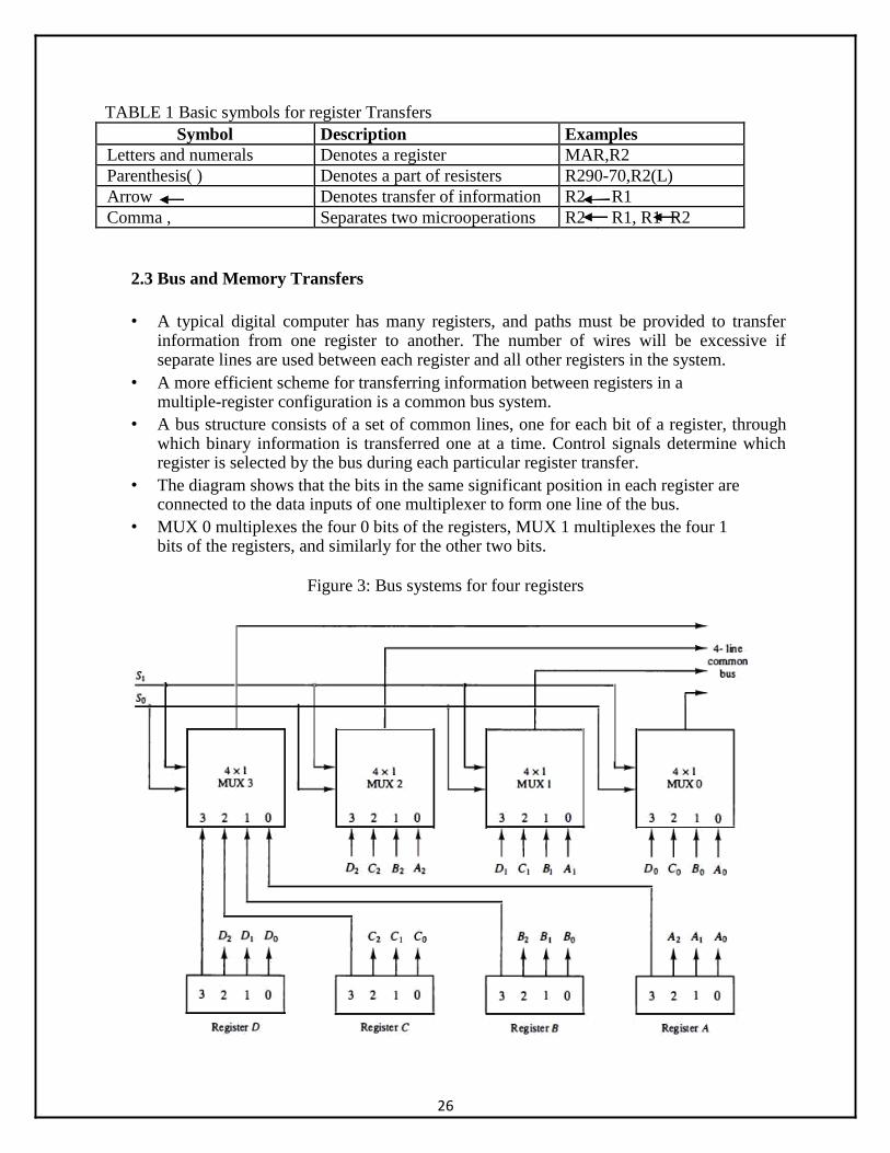
• A bus structure consists of a set of common lines, one for each bit of a register, through which binary information is transferred one at a time. Control signals determine which register is selected by the bus during each particular register transfer.
• The diagram shows that the bits in the same significant position in each register are connected to the data inputs of one multiplexer to form one line of the bus.
• MUX 0 multiplexes the four 0 bits of the registers, MUX 1 multiplexes the four 1 bits of the registers, and similarly for the other two bits.
Figure 3: Bus systems for four registers
26
• The two selection lines S1 and S0 are connected to the selection inputs of all four multiplexers. The selection lines choose the four bits of one register and transfer them into the four-line common bus.
• When S1S0 = 00, the 0 data inputs of all four multiplexers are selected and applied to the outputs that form the bus.
• This causes the bus lines to receive the content of register A since the outputs of this register are connected to the 0 data inputs of the multiplexers. Similarly, register B is selected if S1S0 = 01, and so on.
Table 2 shows the register that is selected by the bus for each of the four possible binary value of the selection lines.
Table 2 function table for Bus of fig 3
S1 S0 Registers selected
0 0 A
0 1 B
1 0 C
1 1 D
• In general, a bus system will multiplex k registers of n bits each to produce an n-line common bus.
• The number of multiplexers needed to construct the bus is equal to n, the number of bits in each register. The size of each multiplexer must be k x 1 since it multiplexes k data lines. For example, a common bus for eight registers of 16 bits each requires 16 multiplexers, one for each line in the bus.
• Each multiplexer must have eight data input lines and three selection lines to multiplex one significant bit in the eight registers.
• The transfer of information from a bus into one of many destination registers can be accomplished by connecting the bus lines to the inputs of all destination registers and activating the load control of the particular destination register selected.
• The symbolic statement for a bus transfer may mention the bus or its presence may be implied in the statement. When the bus is includes in the statement, the register transfer is symbolized as follows:
BUS C, R1 BUS The content of register C is placed on the bus, and the content of the bus is loaded into register R 1 by activating its load control input. If the bus is known to exist in the system, it may be convenient just to show the
direct transfer. R1 C From this statement the designer knows which control signals must be activated to produce the transfer through the bus.
27
Three state bus buffers
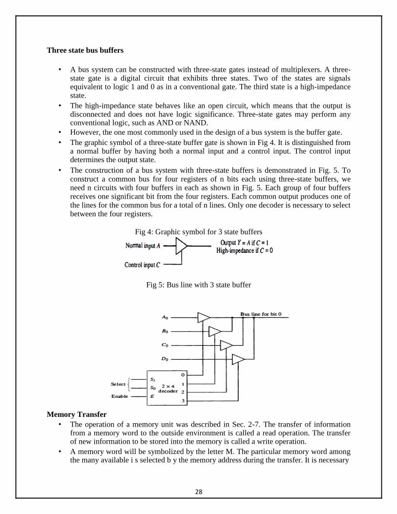
• A bus system can be constructed with three-state gates instead of multiplexers. A three-state gate is a digital circuit that exhibits three states. Two of the states are signals equivalent to logic 1 and 0 as in a conventional gate. The third state is a high-impedance state.
• The high-impedance state behaves like an open circuit, which means that the output is disconnected and does not have logic significance. Three-state gates may perform any conventional logic, such as AND or NAND.
• However, the one most commonly used in the design of a bus system is the buffer gate. • The graphic symbol of a three-state buffer gate is shown in Fig 4. It is distinguished from
a normal buffer by having both a normal input and a control input. The control input determines the output state.
• The construction of a bus system with three-state buffers is demonstrated in Fig. 5. To construct a common bus for four registers of n bits each using three-state buffers, we need n circuits with four buffers in each as shown in Fig. 5. Each group of four buffers receives one significant bit from the four registers. Each common output produces one of the lines for the common bus for a total of n lines. Only one decoder is necessary to select between the four registers.
Fig 4: Graphic symbol for 3 state buffers
Fig 5: Bus line with 3 state buffer
Memory Transfer
• The operation of a memory unit was described in Sec. 2-7. The transfer of information from a memory word to the outside environment is called a read operation. The transfer of new information to be stored into the memory is called a write operation.
• A memory word will be symbolized by the letter M. The particular memory word among the many available i s selected b y the memory address during the transfer. It is necessary
28
to specify the address of M when writing memory transfer operations. This will be done by enclosing the address in square brackets following the letter M .Consider a memory unit that receives the address from a register, called the address register, symbolized by AR . The data are transferred to another register, called the data register, symbolized by DR . The read operation can be stated as follows:
Read: DR [AR] This causes a transfer of information into DR from the memory word M selected by the address in AR .The write operation transfers the content of a data register to a memory word M selected
by the address. Assume that the input data are in register R l R3 R1 +¯R2+ 1
R2 is the symbol for the 1' s complement of R2. Adding 1 to the 1' s complement produces the 2' s complement. Adding the contents of R 1 to the 2' s complement of R2 is equivalent to R1 - R2.
• The increment and decrement microoperations are symbolized by plus one and minus-one operations, respectively. These microoperations are implemented with a combinational circuit or with a binary up-down counter.
• The arithmetic operations of multiply and divide are not listed in Table 3. These two operations are valid arithmetic operations but are not included in the basic set of microoperations.
• The only place where these operations can be considered as microoperations is in a digital system, where they are implemented by means of a combinational circuit.
2.4 Arithmetic micro operations
Binary Adder
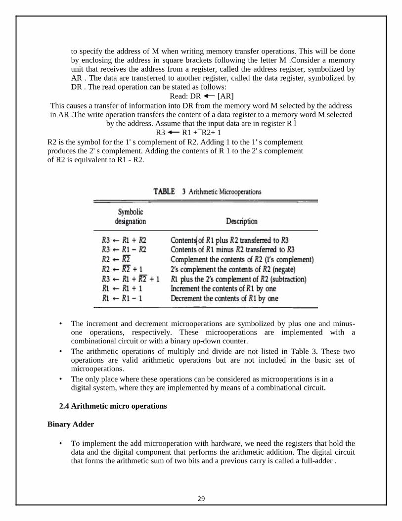
• To implement the add microoperation with hardware, we need the registers that hold the data and the digital component that performs the arithmetic addition. The digital circuit that forms the arithmetic sum of two bits and a previous carry is called a full-adder .
29
• The digital circuit that generates the arithmetic sum of two binary numbers of any length
is called a binary adder. • The binary adder is constructed with full-adder circuits connected in cascade, with the
output carry from one full-adder connected to the input carry of the next full-adder. Figure 4-6 shows the interconnections of four full-adders (FA) to provide a 4-bit binary adder.
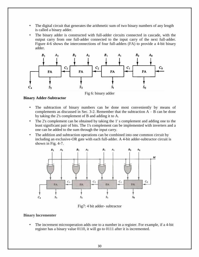
Fig 6: binary adder Binary Adder-Subtractor
• The subtraction of binary numbers can be done most conveniently by means of complements as discussed in Sec. 3-2. Remember that the subtraction A – B can be done by taking the 2's complement of B and adding it to A.
• The 2's complement can be obtained by taking the 1' s complement and adding one to the least significant pair of bits. The 1's complement can be implemented with inverters and a one can be added to the sum through the input carry.
• The addition and subtraction operations can be combined into one common circuit by including an exclusive-OR gate with each full-adder. A 4-bit adder-subtractor circuit is shown in Fig. 4-7.
Fig7: 4 bit adder- subtractor
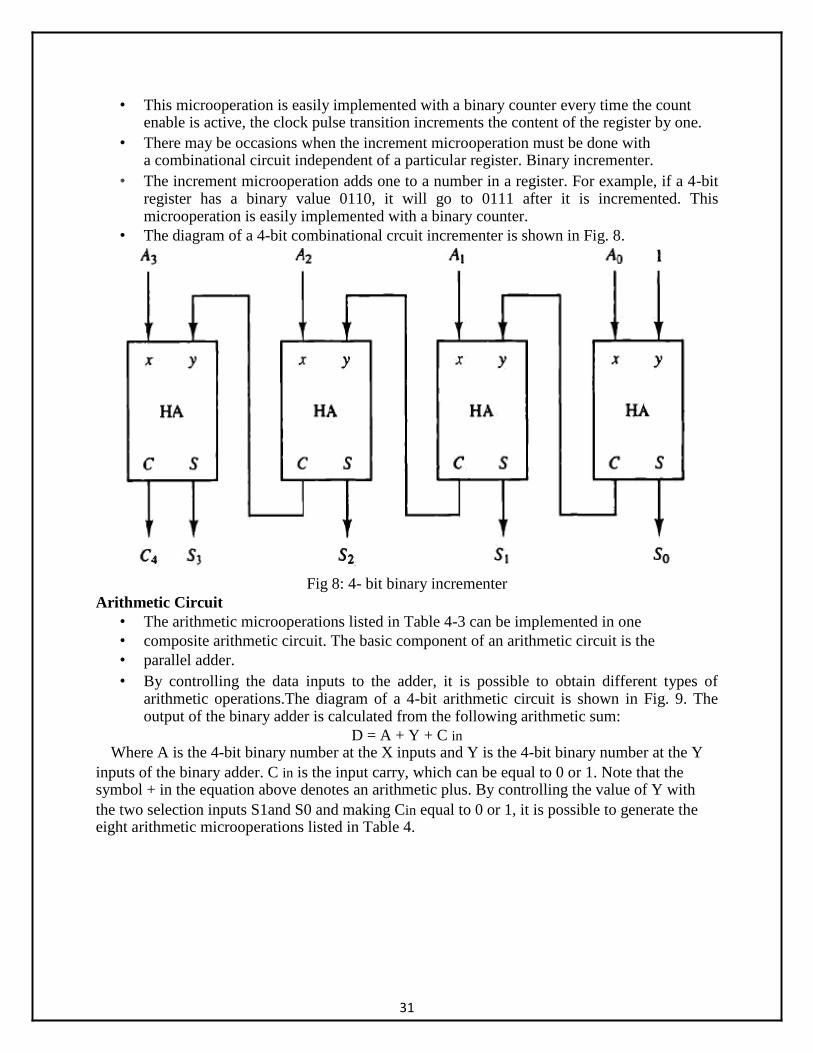
Binary lncrementer
• The increment microoperation adds one to a number in a register. For example, if a 4-bit register has a binary value 0110, it will go to 0111 after it is incremented.
30
• This microoperation is easily implemented with a binary counter every time the count
enable is active, the clock pulse transition increments the content of the register by one. • There may be occasions when the increment microoperation must be done with
a combinational circuit independent of a particular register. Binary incrementer. • The increment microoperation adds one to a number in a register. For example, if a 4-bit
register has a binary value 0110, it will go to 0111 after it is incremented. This microoperation is easily implemented with a binary counter.
• The diagram of a 4-bit combinational crcuit incrementer is shown in Fig. 8.
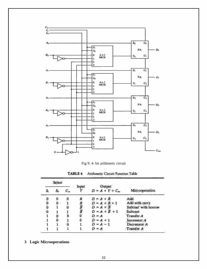
Fig 8: 4- bit binary incrementer Arithmetic Circuit
• The arithmetic microoperations listed in Table 4-3 can be implemented in one • composite arithmetic circuit. The basic component of an arithmetic circuit is the • parallel adder. • By controlling the data inputs to the adder, it is possible to obtain different types of
arithmetic operations.The diagram of a 4-bit arithmetic circuit is shown in Fig. 9. The output of the binary adder is calculated from the following arithmetic sum:
D = A + Y + C in
Where A is the 4-bit binary number at the X inputs and Y is the 4-bit binary number at the Y inputs of the binary adder. C in is the input carry, which can be equal to 0 or 1. Note that the symbol + in the equation above denotes an arithmetic plus. By controlling the value of Y with the two selection inputs S1and S0 and making Cin equal to 0 or 1, it is possible to generate the eight arithmetic microoperations listed in Table 4.
31
Fig 9: 4- bit arithmetic circuit
3 Logic Microoperations
32
Logic microoperations specify binary operations for strings of bits stored in registers. These operations consider each bit of the register separately and treat them as binary variables. For example, the exclusive-OR microoperation with the contents of two registers R 1 and R2 is symbolized by the statement
P: R1 +- R1 ⊕ R2 It specifies a logic microoperation to be executed on the individual bits of the registers provided that the control variable P = 1. As a numerical example, assume that each register has four bits. Let the content of R1 be 1010 and the content of R2 be 1 100. The exclusive-OR microoperation stated above symbolizes the following logic computation:
1010 Content of R 1
1 100 Content of R2
0110 Content of R 1 after P = 1 The content of R 1 , after the execution of the microoperation, is equal to the bit-by-bit exclusive-OR operation on pairs of bits in R2 and previous values of R l . The logic microoperations are seldom used in scientific computations, but they are very useful for bit manipulation of binary data and for making logical decisions.
• Special symbols will be adopted for the logic microoperations OR, AND, and complement, to distinguish them from the corresponding symbols used to express Boolean functions.
• The symbol V will be used to denote an OR microoperation and the symbol 1\ to denote an AND microoperation. The complement microoperation is the same as the 1's complement and uses a bar on top of the symbol that denotes the register name.
• By using different symbols, it will be possible to differentiate between a logic microoperation and a control (or Boolean) function. Another reason for adopting two
sets of symbols is to be able to distinguish the symbol + , when used to symbolize an
arithmetic plus, from a logic OR operation. Although the + symbol has two meanings, it
will be possible to distinguish between them by noting where the symbol occurs.
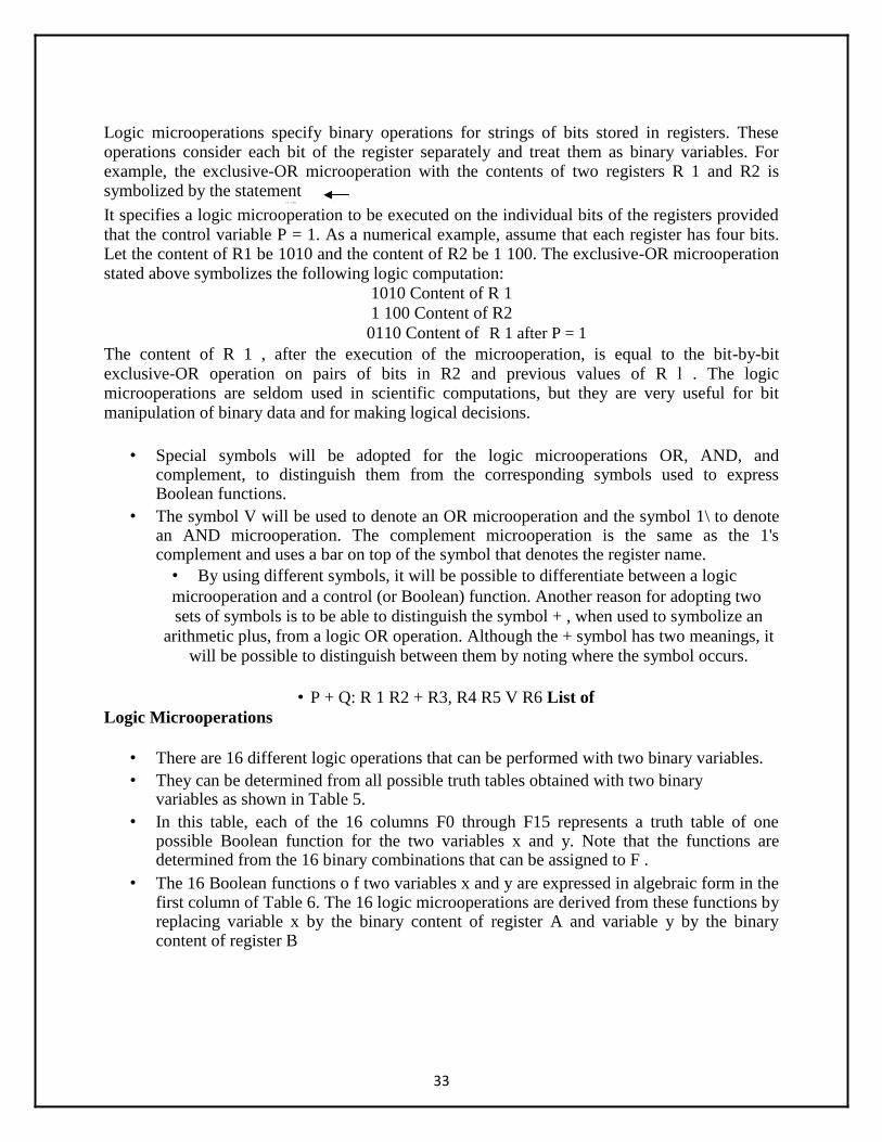
• P + Q: R 1 R2 + R3, R4 R5 V R6 List of Logic Microoperations
• There are 16 different logic operations that can be performed with two binary variables. • They can be determined from all possible truth tables obtained with two binary
variables as shown in Table 5. • In this table, each of the 16 columns F0 through F15 represents a truth table of one
possible Boolean function for the two variables x and y. Note that the functions are determined from the 16 binary combinations that can be assigned to F .
• The 16 Boolean functions o f two variables x and y are expressed in algebraic form in the first column of Table 6. The 16 logic microoperations are derived from these functions by replacing variable x by the binary content of register A and variable y by the binary content of register B
33
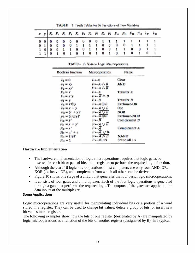
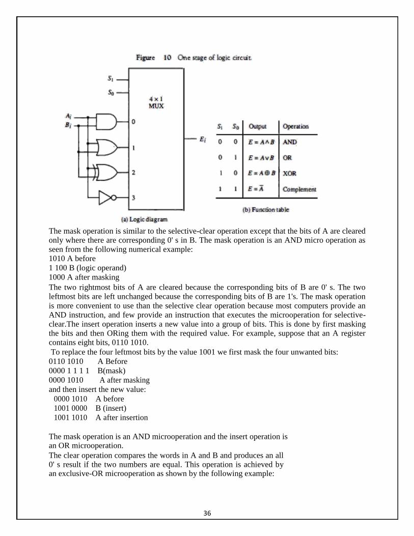
Hardware Implementation
• The hardware implementation of logic rnicrooperations requires that logic gates be inserted for each bit or pair of bits in the registers to perform the required logic function.
• Although there are 16 logic rnicrooperations, most computers use only four-AND, OR, XOR (exclusive-OR), and complementfrom which all others can be derived.
• Figure 10 shows one stage of a circuit that generates the four basic logic rnicrooperations. • It consists of four gates and a multiplexer. Each of the four logic operations is generated
through a gate that performs the required logic.The outputs of the gates are applied to the data inputs of the multiplexer.
Some Applications
Logic microoperations are very useful for manipulating individual bits or a portion of a word stored in a register. They can be used to change bit values, delete a group of bits, or insert new bit values into a register. The following examples show how the bits of one register (designated by A) are manipulated by logic rnicrooperations as a function of the bits of another register (designated by B). In a typical
34
application, register A is a processor register and the bits of register B constitute a logic operand extracted from memory and placed in register B . The selective-set operation sets t o 1 the bits in register A where there are corresponding 1's in register B. It does not affect bit positions that have D's in B. The following numerical example clarifies this operation:
1010 A before
1100 B (logic operand)
1110 A after The two leftmost bits of B are 1' s, so the corresponding bits of A are set to 1 .One o f these two bits was already set and the other has been changed from 0 to1. The two bits of A with corresponding 0' s in B remain unchanged. The example above serves as a truth table since it has all four possible combinations of two binary variables. From the truth table we note that the bits of A after the operation are obtained from the logic-OR operation of bits in B and previous values of A. Therefore, the OR rnicrooperation can be used to selectively set bits of a register.
The selective-complement operation complements bits in A where there are selective-clear corresponding l's in B . It does not affect bit positions that have D's in B . For example:
1010 A before
1100 B (logic operand)
0110 A after Again the two leftmost bits of B are 1's, so the corresponding bits of A are complemented. This
example again can serve as a truth table from which one can deduce that the selective-complement operation is just an exclusive-OR rnicrooperation. Therefore, the exclusive-OR
rnicrooperation can be used to selectively complement bits of a register.The selective-clear
operation clears to 0 the bits in A only where there are corresponding 1's in B. For example:
1010 A before
1 100 B (logic operand)
0 010 A after Again the two leftmost bits of B are 1' s, so the corresponding bits of A are cleared to 0. One can deduce that the Boolean operation performed on the individual bits is AB ' . The corresponding logic rnicrooperation is A A /\ B.
35
The mask operation is similar to the selective-clear operation except that the bits of A are cleared only where there are corresponding 0' s in B. The mask operation is an AND micro operation as seen from the following numerical example: 1010 A before
1 100 B (logic operand)
1000 A after masking The two rightmost bits of A are cleared because the corresponding bits of B are 0' s. The two leftmost bits are left unchanged because the corresponding bits of B are 1's. The mask operation
is more convenient to use than the selective clear operation because most computers provide an AND instruction, and few provide an instruction that executes the microoperation for selective-clear.The insert operation inserts a new value into a group of bits. This is done by first masking the bits and then ORing them with the required value. For example, suppose that an A register contains eight bits, 0110 1010. To replace the four leftmost bits by the value 1001 we first mask the four unwanted bits:
0110 1010 A Before
0000 1 1 1 1 B(mask)
0000 1010 A after masking
and then insert the new value: 0000 1010 A before
1001 0000 B (insert)
1001 1010 A after insertion
The mask operation is an AND microoperation and the insert operation is an OR microoperation. The clear operation compares the words in A and B and produces an all 0' s result if the two numbers are equal. This operation is achieved by an exclusive-OR microoperation as shown by the following example:
36
1010 A
1010 B
0000 A <-A + B
When A and B are equal, the two corresponding bits are either both 0 or both 1. In either case the exclusive-OR operation produces a 0. The all-O's result is then checked to determine if the two numbers were equal.
2.5 Shift Microoperations
• Shift rnicrooperations are used for serial transfer of data. They are also used in conjunction with arithmetic, logic, and other data-processing operations.
• The contents of a register can be shifted to the left or the right. At the same time that the bits are shifted, the first flip-flop receives its binary information from the serial input. During a shift-left operation the serial input transfers a bit into the rightmost position. During a shift-right operation the serial input transfers a bit into the leftmost position.
• The information transferred through the serial input determines the type of shift. There are three types of shifts: logical, circular, and arithmetic.
• A logical shift is one that transfers 0 through the serial input. We will adopt the symbols shl and shr for logical shift-left and shift-right rnicrooperations. For example:
R1 s hl R1
R2 shr R2 are two rnicrooperations that specify a 1-bit shift to the left of the content of register R 1 and a 1-bit shift to the right of the content of register R2.The symbolic notation for the shift rnicrooperations is shown in table 7.
• An arithmetic shift is a rnicrooperation that shifts a signed binary number to the left or right. An arithmetic shift-left multiplies a signed binary number by 2.
• An arithmetic shift-right divides the number by 2. Arithmetic shifts must leave the sign bit unchanged because the sign of the number remains the same when it is multiplied or divided by 2. The leftmost bit in a register holds the sign bit, and the remaining bits hold the number.
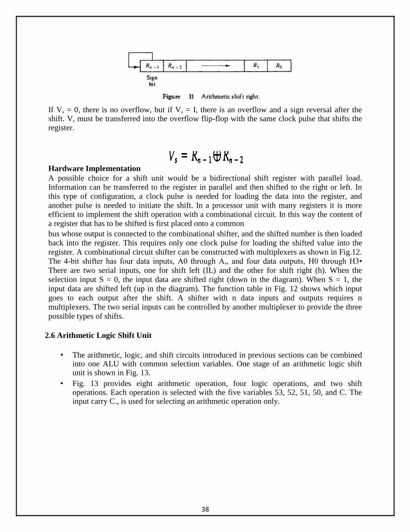
37
If V, = 0, there is no overflow, but if V, = I, there is an overflow and a sign reversal after the shift. V, must be transferred into the overflow flip-flop with the same clock pulse that shifts the register.
Hardware Implementation A possible choice for a shift unit would be a bidirectional shift register with parallel load. Information can be transferred to the register in parallel and then shifted to the right or left. In this type of configuration, a clock pulse is needed for loading the data into the register, and another pulse is needed to initiate the shift. In a processor unit with many registers it is more efficient to implement the shift operation with a combinational circuit. In this way the content of a register that has to be shifted is first placed onto a common bus whose output is connected to the combinational shifter, and the shifted number is then loaded back into the register. This requires only one clock pulse for loading the shifted value into the
register. A combinational circuit shifter can be constructed with multiplexers as shown in Fig.12. The 4-bit shifter has four data inputs, A0 through A,, and four data outputs, H0 through H3•
There are two serial inputs, one for shift left (IL) and the other for shift right (h). When the selection input S = 0, the input data are shifted right (down in the diagram). When S = 1, the
input data are shifted left (up in the diagram). The function table in Fig. 12 shows which input
goes to each output after the shift. A shifter with n data inputs and outputs requires n multiplexers. The two serial inputs can be controlled by another multiplexer to provide the three
possible types of shifts.
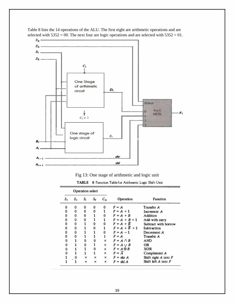
2.6 Arithmetic Logic Shift Unit
• The arithmetic, logic, and shift circuits introduced in previous sections can be combined into one ALU with common selection variables. One stage of an arithmetic logic shift unit is shown in Fig. 13.
• Fig. 13 provides eight arithmetic operation, four logic operations, and two shift operations. Each operation is selected with the five variables 53, 52, 51, 50, and C. The input carry C., is used for selecting an arithmetic operation only.
38
Table 8 lists the 14 operations of the ALU. The first eight are arithmetic operations and are
selected with 5352 = 00. The next four are logic operations and are selected with 5352 = 01.
Fig 13: One stage of arithmetic and logic unit
39
2.7 Control memory
• the control memory can be a read-only memory (ROM).The content of the words in ROM are fixed and cannot be altered by simple programming since no writing capability is available in the ROM.
• ROM words are made permanent during the hardware production of the unit. The use of a microprogram involves placing all control variables in words of ROM for use by the control unit through successive read operations.
• The content of the word in ROM at a given address specifies a microinstruction.A more advanced development known as dynamic microprogramming
• permits a microprogram to be loaded initially from an auxiliary memory such as a magnetic disk. Control units that use dynamic microprogramming employ a writable control memory.
• This type of memory can be used for writing (to change the microprogram) but is used mostly for reading. A memory that is part of a control unit is referred to as a control memory.
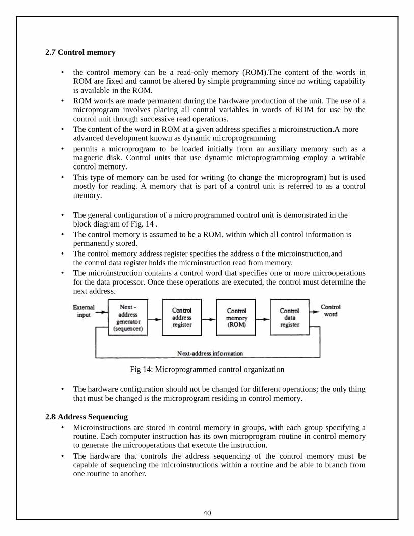
• The general configuration of a microprogrammed control unit is demonstrated in the
block diagram of Fig. 14 . • The control memory is assumed to be a ROM, within which all control information is
permanently stored. • The control memory address register specifies the address o f the microinstruction,and
the control data register holds the microinstruction read from memory. • The microinstruction contains a control word that specifies one or more microoperations
for the data processor. Once these operations are executed, the control must determine the next address.
Fig 14: Microprogrammed control organization
• The hardware configuration should not be changed for different operations; the only thing that must be changed is the microprogram residing in control memory.
2.8 Address Sequencing
• Microinstructions are stored in control memory in groups, with each group specifying a routine. Each computer instruction has its own microprogram routine in control memory to generate the microoperations that execute the instruction.
• The hardware that controls the address sequencing of the control memory must be capable of sequencing the microinstructions within a routine and be able to branch from one routine to another.
40
• To appreciate the address sequencing in a microprogram control unit, let us enumerate
the steps that thecontrol must undergo during the execution of a single computer instruction.An initial address is loaded into the control address register when power is turned on in the computer.
• This address is usually the address of the first microinstruction that activates the instruction fetch routine.
• The fetch routine may be sequenced by incrementing the control address register through the rest of its microinstructions. At the end of the fetch routine, the instruction isin the instruction register of the computer.
The next step is to generate the microoperations that execute the instruction fetched from memory.
• The microoperation steps to be generated in processor registers depend on the operation code part of the instruction. Each instruction has its own microprogram routine stored in a given location of control memory.
• The transformation from the instruction code bits to an address in control memory where the routine is located is referred to as a mapping process. A mapping procedure is a rule that transforms the instruction code into a control memory address.
• Once the required routine is reached, the microinstructions that execute the instruction may be sequenced by incrementing the control address register, but sometimes the sequence of microoperalions will depend on values of certain status bits in processor registers .
• Microprograms that employ subroutines will require an external register for storing the return address.
• Return addresses cannot be stored in ROM because the unit has no writing capability. • When the execution of the instruction is completed, control must return to the fetch
routine. • This is accomplished by executing an unconditional branch microinstruction to the
first address of the fetch routine.
In summary, the address sequencing capabilities required in a control memory are:
1. Incrementing of the control address register. 2. Unconditional branch or conditional branch, depending on status bit conditions. 3. A mapping process from the bits of the instruction to an address for control memory. 2. A facility for subroutine call and return.
Figure 7-2 shows a block diagram of a control memory and the associated hardware needed for selecting the next microinstruction address. Conditional Branching The branch logic of Fig. 15 provides decision-making capabilities in the control unit. The status conditions are special bits in the system that provide parameter information such as the carry-out of an adder, the sign bit of a number, the mode bits of an instruction, and input or output status conditions..
41
Fig 15: Selection for address for control memory
Mapping of Instruction • A special type of branch exists when a microinstruction specifies a branch to the first
word in control memory where a microprogram routine for an instruction is located. • The status bits for this type of branch are the bits in the operation code part of the
instruction. For example, a computer with a simple instruction format as shown in Fig. 16 has an operation code of four bits which can specify up to 16 distinct instructions.
• Assume further that the control memory has 128 words, requiring an address of seven bits. For each operation code there exists a microprogram routine in control memory that executes the instruction. One simple mapping process that converts the 4-bit operation code to a 7-bit address for control memory is shown in Fig. 16.
• This mapping consists of placing a 0 in the most significant bit of the address, transferring the four operation code bits, and clearing the two least significant bits of the control address register. This provides for each computer instruction a microprogram routine with a capacity of four microinstructions. If the routine needs more than four microinstructions, it can use addresses 1000000 through 1 1 1 1 1 1 1 .
42
Fig 16: mapping of instructions Subroutines
• Subroutines are programs that are used by other routines to accomplish a particular task. A subroutine can be called from any point within the main body of the microprogram.
• Frequently, many microprograms contain identical sections of code. Microinstructions can be saved by employing subroutines that use common sections of microcode. For example, the sequence of microoperations needed to generate the effective address of the operand for an instruction is common to all memory reference instructions. This sequence could be a subroutine that is called from within many other routines to execute the effective address computation.
• Microprograms that use subroutines must have a provision for storing the return address during a subroutine call and restoring the address during a subroutine return.
Microprogram Example Once the configuration of a computer and its microprogrammed control unit is established, the designer's task is to generate the microcode for the control memory. This code generation is called microprogramming and is a process similar to conventional machine language programming.
Computer Configuration
The block diagram of the computer is shown in Fig. 17 It consists of two memory units: a main memory for storing instructions and data, and a control memory for storing the microprogram. Four registers are associated with the processor unit and two with the control unit. The processor registers are
43
Fig 17 computer hard ware configuration
program counter PC, address register AR, data register DR, and accumulator register AC. The function of these registers is similar to the basic computer
2.8 Design of Control Unit
• The bits of the microinstruction are usually divided into fields, with each field defining a distinct, separate function. The various fields encountered in instruction formats provide control bits to initiate microoperations in the system, special bits to specify the way that the next address is to be evaluated, and an address field for branching.
• The number of control bits that initiate microoperations can be reduced by grouping mutually exclusive variables into fields and encoding the k bits in each field to provide 2' microoperations. Each field requires a decoder to produce the corresponding control signals.
• This method reduces the size of the microinstruction bits but requires additional hardware external to the control memory. It also increases the delay time of the control signals because they must propagate through the decoding circuits.
44
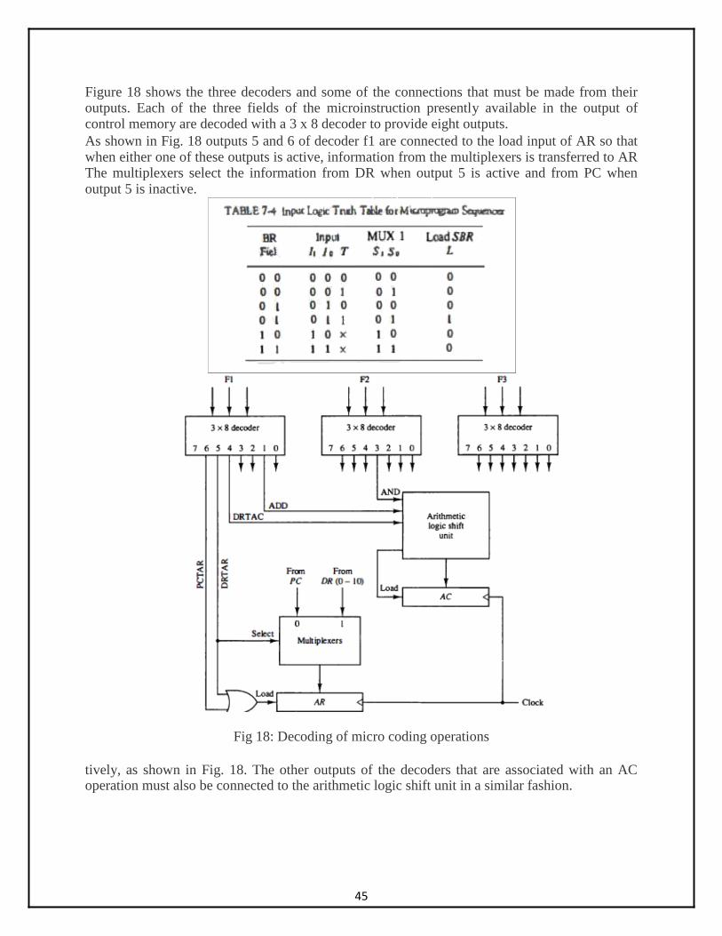
Figure 18 shows the three decoders and some of the connections that must be made from their outputs. Each of the three fields of the microinstruction presently available in the output of control memory are decoded with a 3 x 8 decoder to provide eight outputs. As shown in Fig. 18 outputs 5 and 6 of decoder f1 are connected to the load input of AR so that when either one of these outputs is active, information from the multiplexers is transferred to AR The multiplexers select the information from DR when output 5 is active and from PC when output 5 is inactive.
Fig 18: Decoding of micro coding operations
tively, as shown in Fig. 18. The other outputs of the decoders that are associated with an AC operation must also be connected to the arithmetic logic shift unit in a similar fashion.
45
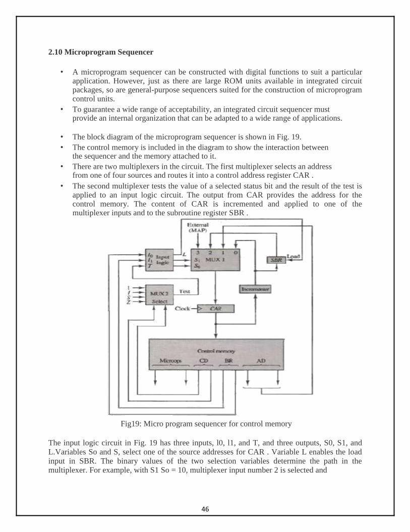
2.10 Microprogram Sequencer
• A microprogram sequencer can be constructed with digital functions to suit a particular application. However, just as there are large ROM units available in integrated circuit packages, so are general-purpose sequencers suited for the construction of microprogram control units.
• To guarantee a wide range of acceptability, an integrated circuit sequencer must provide an internal organization that can be adapted to a wide range of applications.
• The block diagram of the microprogram sequencer is shown in Fig. 19. • The control memory is included in the diagram to show the interaction between
the sequencer and the memory attached to it. • There are two multiplexers in the circuit. The first multiplexer selects an address
from one of four sources and routes it into a control address register CAR . • The second multiplexer tests the value of a selected status bit and the result of the test is
applied to an input logic circuit. The output from CAR provides the address for the control memory. The content of CAR is incremented and applied to one of the multiplexer inputs and to the subroutine register SBR .
Fig19: Micro program sequencer for control memory
The input logic circuit in Fig. 19 has three inputs, l0, l1, and T, and three outputs, S0, S1, and L.Variables So and S, select one of the source addresses for CAR . Variable L enables the load input in SBR. The binary values of the two selection variables determine the path in the multiplexer. For example, with S1 So = 10, multiplexer input number 2 is selected and
46
establishes a transfer path from SBR to CAR. Note that each of the four inputs as well as the output of MUX 1 contains a 7-bit address.
47
UNIT-III
CPU AND COMPUTER ARITHMETIC
CPU design: Instruction cycle, data representation, memory reference instructions, input-
output, and interrupt, addressing modes, data transfer and manipulation, program control.
Computer arithmetic: Addition and subtraction, floating point arithmetic operations, decimal
arithmetic unit.
3.1 INSTRUCTION CYCLE
• An instruction cycle (sometimes called a fetch–decode–execute cycle) is the basic operational process of a computer.
• It is the process by which a computer retrieves a program instruction from its memory,
determines what actions the instruction dictates, and carries out those actions.
• This cycle is repeated continuously by a computer's central processing unit (CPU), from boot-up to when the computer is shut down.
• In simpler CPUs the instruction cycle is executed sequentially, each instruction being
processed before the next one is started.
• In most modern CPUs the instruction cycles are instead executed concurrently, and often in parallel, through an instruction pipeline: the next instruction starts being processed before the previous instruction has finished, which is possible because the cycle is broken up into separate steps.
COMPONENTS
Program counter (PC)
An incrementing counter that keeps track of the memory address of the instruction that is to be executed next or in other words, holds the address of the instruction to be executed next.
Memory address registers (MAR)
Holds the address of a block of memory for reading from or writing to.
Memory data register (MDR)
A two-way register that holds data fetched from memory (and ready for the CPU to process) or
data waiting to be stored in memory. (This is also known as the memory buffer register (MBR).
Instruction register (IR)
48
A temporary holding ground for the instruction that has just been fetched from memory.
Control unit (CU)
Decodes the program instruction in the IR, selecting machine resources, such as a data source
register and a particular arithmetic operation, and coordinates activation of those resources.
Arithmetic logic unit (ALU)
Performs mathematical and logical operations.
Floating-point unit (FPU)
Performs floating-point operations.
Each computer's CPU can have different cycles based on different instruction sets, but will be similar to the following cycle:
1. Fetch the instruction: The next instruction is fetched from the memory address that is
currently stored in the program counter (PC), and stored in the instruction register (IR). At the end of the fetch operation, the PC points to the next instruction that will be read at the next cycle.
2. Decode the instruction: During this cycle the encoded instruction present in the IR (instruction register) is interpreted by the decoder.
3. Read the effective address: In case of a memory instruction (direct or indirect) the execution phase will be in the next clock pulse. If the instruction has an indirect address, the effective address is read from main memory, and any required data is fetched from
main memory to be processed and then placed into data registers (Clock Pulse: T3). If the instruction is direct, nothing is done at this clock pulses. If this is an I/O instruction or a Register instruction, the operation is performed (executed) at clock Pulse.
4. Execute the instruction: The control unit of the CPU passes the decoded information as
a sequence of control signals to the relevant function units of the CPU to perform the
actions required by the instruction such as reading values from registers, passing them to the ALU to perform mathematical or logic functions on them, and writing the result back
to a register. If the ALU is involved, it sends a condition signal back to the CU. The result generated by the operation is stored in the main memory, or sent to an output
device. Based on the condition of any feedback from the ALU, Program Counter may be updated to a different address from which the next instruction will be fetched.
The cycle is then repeated.
Initiating the cycle
The cycle begins as soon as power is applied to the system, with an initial PC value that is predefined by the system's architecture (for instance, in Intel IA-32 CPUs, the predefined PC value is ). Typically this address points to a set of instructions in read-only memory (ROM), which begins the process of loading (or booting) the operating system.
49
Fetching the instruction
Step 1 of the instruction cycle is fetch cycle, which is the same for each instruction:
1. The CPU sends the PC to the MAR and sends a read command on the address bus 2. In response to the read command (with address equal to PC), the memory returns the
data stored at the memory location indicated by PC on the data bus 3. The CPU copies the data from the data bus into its MDR (also known as MBR, see
section Components above) 4. A fraction of a second later, the CPU copies the data from the MDR to the
instruction register (IR) 5. The PC is incremented so that it points to the following instruction in memory. This step
prepares the CPU for the next cycle.
The control unit fetches the instruction's address from the memory unit.
Decoding the instruction
Step 2 of the instruction Cycle is called the Decode Cycle. The decoding process allows the CPU to determine what instruction is to be performed, so that the CPU can tell how many operands it needs to fetch in order to perform the instruction. The opcode fetched from the memory is decoded for the next steps and moved to the appropriate registers. The decoding is done by the CPU's Control Unit.
Reading the effective address
Step 3 is evaluating which operation it is. If this is a Memory operation - in this step the computer checks if it's a direct or indirect memory operation:
• Direct memory instruction - Nothing is being done. • Indirect memory instruction - The effective address is being read from the memory.
If this is an I/O or Register instruction - the computer checks its kind and executes the instruction.
Executing the instruction
Step 4 of the Instruction Cycle is the Execute Cycle. Here, the function of the instruction is performed. If the instruction involves arithmetic or logic, the Arithmetic Logic Unit is utilized. This is the only stage of the instruction cycle that is useful from the perspective of the end user. Everything else is overhead required to make the execute phase happen.
3.2 DATA REPRESENTATION
3.1.2 DATA TYPES
The data types found in the registers of digital computers may be classified as being one of the
following categories:
• numbers used in arithmetic computations,
• letters of the alphabet used in data processing.
50
• Other discrete symbols used for specific purposes.
All types of data, except binary numbers, are represented in computer registers in binary form.
This is because registers are made up of flip-flops and flip-flops are two-state devises that can
store only l's and O's.
The binary number system is the most natural system to use in a digital computer. But sometimes
it is convenient to employ different number systems.
Number systems
• A number system of base, or radix, r is a system that uses distinct symbols for r digits. Numbers are represented by a string of digit symbols.
• To determine the quantity that the number represents, it is necessary to multiply
each digit by an integer power of r and then form the sum of all weighted digits. For example, the decimal number system in everyday use employs the radix 10 system.
• The 10 symbols are 0, 1, 2, 3, 4, 5, 6, 7, 8, and 9. The string of digits
• 724.5 is interpreted to represent the quantity
• 7 X 10² + 2 X 101 + 4 X 10° + 5 X 10⁻¹
The binary number system uses the radix 2. The two digit symbols used are 0 and 1. The string of digits 101101 is interpreted to represent the quantity
To distinguish between different radix numbers, the digits will be enclosed in parentheses and the radix of the number inserted as a subscript. For example, to show the equality between
decimal and binary forty-five we will write (101101)2 = (45)10.
The octal (radix 8) and hexadecimal (radix 16) are important in digital computer work. The eight symbols of the octal system are 0, 1, 2, 3, 4, 5, 6, and 7. The 16 symbols of the hexadecimal system are 0, 1, 2, 3, 4, 5, 6, 7, 8, 9, A, B, C, 0, E, and F. When used to represent hexadecimal digits, the symbols A, B, C, D, E, F correspond to the decimal numbers 10, 11, 12, 13, 14, 15, respectively.
Octal 736.4 is converted to decimal as follows:
51
The equivalent decimal number of hexadecimal F3 is obtained from the following calculation:
The basic computer has three 16-bit instruction code formats:
1. Memory Reference Instructions
2. Register Reference Instructions
3. Input/Output Instructions
MEMORY REFERENCE INSTRUCTIONS
In Memory reference instruction: First 12 bits(0-11) specify an address. Next 3 bits specify operation code (opcode). Left most bit specify the addressing mode I
I = 0 for direct address I = 1 for indirect address
Memory Reference Instructions
In Memory reference instruction: first 12 bits (0-11) specify an address. The address field is denoted by three x’s (in hexadecimal notation) and is equivalent to 12-bit
address. The last mode bit of the instruction represents by symbol I. When I = 0, the last four bits of an instruction have a
hexadecimal digit equivalent from 0 to 6 since the last bit is zero (0). When I = 1 the last four bits of an instruction have a hexadecimal digit equivalent from 8 to E since the last bit is one (1).
Memory Reference Instructions
Hexadecimal code
Symbol I = 0 I = 1 Description
AND 0xxx 8xxx AND memory word to AC
ADD 1xxx 9xxx ADD memory word to AC
LDA 2xxx Axxx LOAD Memory word to AC
STA 3xxx Bxxx Store content of AC in memory
BUN 4xxx Cxxx Branch unconditionally
BSA 5xxx Dxxx Branch and save return address
53
ISZ 6xxx Exxx Increment and Skip if zero
Register Reference Instructions
In Register Reference Instruction: First 12 bits (0-11) specify the register operation. The next three bits equals to 111 specify opcode. The last mode bit of the instruction is 0.
Therefore, left most 4 bits are always 0111 which is equal to hexadecimal 7.
I/O Reference Instructions
In I/O Reference Instruction: First 12 bits (0-11) specify the I/O operation. The next three bits equals to 111 specify opcode. The last mode bit of the instruction is 1.
Therefore, left most 4 bits are always 1111 which is equal tohexadecimal F.
• A computer is useless unless the information is communication between I/O terminals and the processor.In a computer, instructions and data stored in memory come from some input device and computational results must be transmitted to the user through some output device.
• The terminal sends and receives serial information. Each quantity of information
has 8 bits of an alphanumeric code. Two basic computer resisters INPR and OUTR communicate with a communication interface.
Input-Output Configuration
54
• The terminals send and receive serial information the 8-bits information is shifted from
the keyboard into the input register(INPR). The serial • information for the printer is stored in OUTR. These two registers communicate in
the communication interface serially and with the • accumulator in parallel. The transmitter interface receives the information and transfer
to INPR. The receiver interface receives from OUTR and transmits to the printer. • The input register INPR consists of 8-bits and stores alphanumeric information. FGI is 1-
bit controlled flip-flop or flag. A flag bit is set to 1. • When new information is available in input device and cleared to zero and the
information is accepted by the computer. Initially, the input flag • FGI clear to zero. When a key in a keyboard is pressed , 8-bits alphanumeric code is
shifted into INPR is transferred into accumulator and FGI is cleared to zero. The output flag FGO is initially set to one the computer checks FGO and if it is one(1) then the content of accumulator(AC) is transferred into OUTR and FGO is cleared to zero. Once the content of OUTR is transmitted to the printer FGO is again set to 1. Therefore, if FGO=1, then the data from input device can't be transferred into INPR and similarly, if FGO=0, then the content of AC can't be transferred into OUTR.
Input-Output Instruction I/O instructions are needed to transferring information to and from AC register, for checking the flag bits and for controlling the interrupt
facility.
I/O instruction
Program Interrupt • Input and Output interactions with electromechanical peripheral devices require
huge processing times compared with CPU rocessing times. – I/O (milliseconds) versus CPU (nano/microseconds)
• Interrupts permit other CPU instructions to execute while waiting for I/O to complete.
• The I/O interface, instead of the CPU, monitors the I/O device. • When the interface found that the I/O device is ready for data transfer,it generates an
interrupt request to the CPU • Upon detecting an interrupt, the CPU stops momentarily the task it is doing,branches
to the service routine to process the data transfer,and then returns to the task it was performing.
Interrupt Cycle
This is a hardware implementation of a branch and save return address operation.
55
Flowchart of interrupt cycle
• An alternative to the program controlled procedure is to let the internal device inform the
computer when it is ready for data transfer. At The same time, the processor can execute
other tasks. This method uses the interrupt facility when the computer is w=executing a
program, itdoesn't check the flags.But, when the flag is set , the computer is momentarily
interrupted from executing the current program and is informed that the flag has been set. • In this case, the computer momentarily deviates from what it is executing currently and
starts the I/Otransfer . Once the I/O transfer is complete, the computer returns back to its original job.
• The interrupt enables flip-flop IEN can be set and cleared with two instruction. When IEN is cleared to zero with IOF instruction. Then, the flag can't interrupt the computer , when IEN is set to 1 with ION instruction the computer can be
interrupted. Register transfer operation in interrupt cycle Register Transfer Statements for Interrupt Cycle
-RF/F←1ifIEN(FGI+FGO)T0’T1’T2’↔T0’T1’T2’(IEN)(FGI+FGO):R←1 The fetch and decode phases of the instruction cycle must be modified: Replace T0,T1,T2 with R'T0,R'T1,R'T2 The interrupt cycle: RT0:AR←0,TR←PC RT1:M[AR]←TR,PC←0
RT2:PC←PC+1,IEN←0,R←0,SC← 0
56
Complete Computer Description Flowchart
fig. Instruction cycle including Interrupt cycle
ADDRESSING MODES
Addressing mode is the way of addressing a memory location in instruction. Microcontroller needs data or operands on which the operation is to be performed. The method of specifying source of operand and output of result in an instruction is known as addressing mode.
There are various methods of giving source and destination address in instruction, thus there are various types of Addressing Modes. Here you will find the different types of Addressing Modes that are supported in Micro Controller 8051. Types of Addressing Modes are explained below:
Also Read: Introduction to Microcontroller 8051
57
Types Of Addressing Modes:
Following are the types of Addressing Modes:
• Register Addressing Mode • Direct Addressing Mode • Register Indirect Addressing Mode • Immediate Addressing Mode • Index Addressing Mode • Also Read: How Microcontroller Works
Explanation:
• Register Addressing Mode: In this addressing mode, the source of data or destination of result is Register. In this type of addressing mode the name of the register is given in the instruction where the data to be read or result is to be stored.
Example: ADD A, R5 (The instruction will do the addition of data in Accumulator with data in register R5)
For example,
MOV DX, TAX_RATE ; Register in first operand
MOV COUNT, CX ; Register in second operand
MOV EAX, EBX ; Both the operands are in registers
• Direct Addressing Mode: In this type of Addressing Mode, the address of data to be read is directly given in the instruction. In case, for storing result the address given in instruction is used to store the result.
Example: MOV A, 46H (This instruction will move the contents of memory location 46H to Accumulator)
For example,
BYTE_VALUE DB 150 ; A byte value is defined
WORD_VALUE DW 300 ; A word value is defined
ADD BYTE_VALUE, 65 ; An immediate operand 65 is added
MOV AX, 45H ; Immediate constant 45H is transferred to AX
58
• Mode Register Indirect Addressing: In Register Indirect Addressing Mode, as its name
suggests the data is read or stored in register indirectly. That is, we provide the register in the instruction, in which the address of the other register is stored or which points to other register where data is stored or to be stored.
Example: MOV A, @R0 (This instruction will move the data to accumulator from the register whose address is stored in register R0 ).
Also Read: Architecture of 8051
• Immediate Addressing Mode: In Immediate Addressing Mode, the data immediately follows the instruction. This means that data to be used is already given in the instruction itself.
Example: MOV A, #25H (This instruction will move the data 25H to Accumulator. The #sign show that preceding term is data, not the address.)
• Index Addressing Mode: Offset is added to the base index register to form the effective address if the memory location. This Addressing Mode is used for reading lookup tables in Program Memory. The Address of the exact location of the table is formed by adding the Accumulator Data to the base pointer.
Example: MOVC, @A+DPTR (This instruction will move the data from the memory to Accumulator; the address is made by adding the contents of Accumulator and Data Pointer.
Reading Assignments and Exercises
This section is organized as follows:
3.1. Arithmetic and Logic Operations
3.2. Arithmetic Logic Units and the MIPS ALU
3.3. Boolean Multiplication and Division
3.4. Floating Point Arithmetic
3.5. Floating Point in MIPS
Information contained herein was compiled from a variety of text- and Web-based sources, is intended as a teaching aid only (to be used in conjunction with the required text, and is not to be used for any commercial purpose. A particular thank is given to Dr. Enrique Mafla for his permission to use selected illustrations from his course notes in these Web pages.
In order to secure your understanding of the topics in this section, students should review the discussion of number representation in Section 2.4, especially twos complement.
The ALU is the core of the computer - it performs arithmetic and logic operations on data that not only realize the goals of various applications (e.g., scientific and engineering programs), but also manipulate addresses (e.g., pointer arithmetic). In this section, we will overview algorithms used for the basic arithmetic and logical operations. A key assumption is that twos complement representation will be employed, unless otherwise noted.
3.1.1. Boolean Addition
When adding two numbers, if the sum of the digits in a given position equals or exceeds the modulus, then a carry is propagated. For example, in Boolean addition, if two ones are added, the sum is obviously two (base 10), which exceeds the modulus of 2 for Boolean numbers (B = Z2 = {0,1}, the integers modulo 2). Thus, we record a zero for the sum and propagate a carry valued at one into the next more significant digit, as shown in Figure 3.1.
Figure 3.1. Example of Boolean addition with carry propagation, adapted from [Maf01].
3.1.2. Boolean Subtraction
When subtracting two numbers, two alternatives present themselves. First, one can formulate a
subtraction algorithm, which is distinct from addition. Second, one can negate the subtrahend (i.e.,
in a - b, the subtrahend is b) then perform addition. Since we already know how to perform
addition as well as twos complement negation, the second alternative is more practical. Figure 3.2
illustrates both processes, using the decimal subtraction 12 - 5 = 7 as an example.
Figure 3.2. Example of Boolean subtraction using (a) unsigned binary representation, and (b) addition with twos complement negation - adapted from [Maf01].
Just as we have a carry in addition, the subtraction of Boolean numbers uses a borrow. For example, in Figure 3.2a, in the first (least significant) digit position, the difference 0 - 1 in the one's place is realized by borrowing a one from the two's place (next more significant digit). The borrow is propagated upward (toward the most significant digit) until it is zeroed (i.e., until we encounter a difference of 1 - 0).
3.1.3. Overflow
Overflow occurs when there are insufficient bits in a binary number representation to portray the result of an arithmetic operation. Overflow occurs because computer arithmetic is not closed with respect to addition, subtraction, multiplication, or division. Overflow cannot occur in addition (subtraction), if the operands have different (resp. identical) signs.
To detect and compensate for overflow, one needs n+1 bits if an n-bit number representation is employed. For example, in 32-bit arithmetic, 33 bits are required to detect or compensate for overflow. This can be implemented in addition (subtraction) by letting a carry (borrow) occur into (from) the sign bit. To make a pictorial example of convenient size, Figure 3.3 illustrates the four possible sign combinations of differencing 7 and 6 using a number representation that is four bits long (i.e., can represent integers in the interval [-8,7]).
61
Figure 3.3. Example of overflow in Boolean arithmetic, adapted from [Maf01].
3.1.4. MIPS Overflow Handling
MIPS raises an exception when overflow occurs. Exceptions (or interrupts) act like procedure calls. The register $epc stores the address of the instruction that caused the interrupt, and the instruction
mfc register, $epc
moves the contents of $epc to register. For example, register could be $t1. This is an efficient approach, since no conditional branch is needed to test for overflow.
Two's complement arithmetic operations (add, addi, and sub instructions) raise exceptions on overflow. In contrast, unsigned arithmetic (addu and addiu) instructions do not raise an exception on overflow, since they are used for arithmetic operations on addresses (recall our discussion of
pointer arithmetic in Section 2.6). In terms of high-level languages, C ignores overflows (always usesaddu, addiu, and subu), while FORTRAN uses the appropriate instruction to detect overflow. Figure 3.4 illustrates the use of conditional branch on overflow for signed and unsigned addition operations.
62
Figure 3.4. Example of overflow in Boolean arithmetic, adapted from [Maf01].
3.1.5. Logical Operations Logical operations apply to fields of bits within a 32-bit word, such as bytes or bit fields (in C, as
discussed in the next paragraph). These operations include shift-left and shift-right operations (sll
and srl), as well as bitwise and, or (and, andi, or, ori). As we saw in Section 2, bitwise operations
treat an operand as a vector of bits and operate on each bit position.
C bit fields are used, for example, in programming communications hardware, where manipulation of a bit stream is required. In Figure 3.5 is presented C code for an example communications routine, where a structure called receiver is formed from an 8-bit field called receivedByte and two one-bit fields called ready and enable. The C routine sets receiver.ready to 0 and receiver.enable to 1.
63
Figure 3.5. Example of C bit field use in MIPS, adapted from [Maf01].
Note how the MIPS code implements the functionality of the C code, where the state of the registers $s0 and $s1 is illustrated in the five lines of diagrammed register contents below the code. In particular, the initial register state is shown in the first two lines. The sll instruction loads the contents of $s1 (the receiver) into $s0 (the data register), and the result of this is shown on the second line of the register contents. Next, the srl instruction left-shifts $s0 24 bits, thereby discarding the enable and ready field information, leaving just the received byte. To signal the receiver that the data transfer is completed, the andi and ori instructions are used to set the enable and ready bits in $s1, which corresponds to the receiver. The data in $s0 has already been received and put in a register, so there is no need for its further manipulation.
3.2. Arithmetic Logic Units and the MIPS ALU
Reading Assignments and Exercises
In this section, we discuss hardware building blocks, ALU design and implementation, as well as the design of a 1-bit ALU and a 32-bit ALU. We then overview the implementation of the MIPS ALU.
3.2.1. Basic Concepts of ALU Design
ALUs are implemented using lower-level components such as logic gates, including and, or, not gates and multiplexers. These building blocks work with individual bits,
but the actual ALU works with 32-bit registers to perform a variety of tasks such as arithmetic and shift operations.
In principle, an ALU is built from 32 separate 1-bit ALUs. Typically, one constructs separate hardware blocks for each task (e.g., arithmetic and logical operations), where each operation is applied to the 32-bit registers in parallel, and the selection of an operation is controlled by a multiplexer. The advantage of this approach is that it is easy to add new operations to the instruction set, simply by associating an operation with a multiplexer control code. This can be done provided that the mux has sufficient capacity. Otherwise, new data lines must be added to the mux(es), and the CPU must be modified to accomodate these changes.
3.2.2.1. And/Or Operations. As shown in Figure 3.6, a simple (1-bit) ALU operates in parallel, producing all possible results that are then selected by the multiplexer (represented by an oval shape at the output of the and / or gates. The output C is thus selected by the multiplexer. (Note: If the multiplexer were to be applied at the input(s) rather than the output, twice the amount of hardware would be required, because there are two inputs versus one output.)
Figure 3.6. Example of a simple 1-bit ALU, where the oval represents a multiplexer with a control code denoted by Op and an output denoted by C - adapted from [Maf01].
3.2.2.2. Full Adder. Now let us consider the one-bit adder. Recalling the carry situation
shown in Figure 3.1, we show in Figure 3.7 that there are two types of carries - carry in (occurs at the input) and carry out (at the output).
Figure 3.7. Carry-in and carry-out in Boolean addition, adapted from [Maf01].
65
Here, each bit of addition has three input bits (Ai, Bi, and CarryIni), as well as two output bits (Sumi, CarryOuti), where CarryIn i+1 = CarryOuti. (Note: The "i" subscript denotes the i-th bit.) This relationship can be seen when considering the full adder's truth table, shown below:
Given the four one-valued results in the truth table, we can use the sum-of-products method to construct a one-bit adder circuit from four three-input and gates and one four-input or gate, as shown in Figure 3.8a. The CarryOut calculation can be similarly implemented with three two-input and gates and one three-input or gate, as shown in Figure 3.8b. These two circuits can be combined to effect a one-bit full adder with carry, as shown in Figure 3.8c.
(a) (b)
66
(c)
Figure 3.7. Full adder circuit (a) sum-of-products form from above-listed truth table, (b) CarryOut production, and (c) one-
bit full adder with carry - adapted from [Maf01].
Recalling the symbol for the one-bit adder, we can add an addition operation to the one-bit ALU shown in Figure 3.6. This is done by putting two control lines on the output mux, and by having an additional control line that inverts the b input (shown as "Binvert") in Figure 3.9).
67
(a) (b)
Figure 3.9. One-bit ALU with three operations: and, or, and addition: (a) Least significant bit, (b) Remaining bits - adapted
from [Maf01].
3.2.3. 32-bit ALU Design
The final implementation of the preceding technique is in a 32-bit ALU that incorporates
the and, or, and addition operations. The 32-bit ALU can be simply constructed from the one-bit
ALU by chaining the carry bits, such that CarryIni+1 = CarryOuti, as shown in Figure 3.10.
Figure 3.10. 32-bit ALU with three operations: and, or, and addition - adapted from [Maf01].
This yields a composite ALU with two 32-bit input vectors a and b, whose i-th bit is denoted by ai
and b i, where i = 0..31. The result is also a 32-bit vector, and there are two control buses -
68
one for Binvert, and one for selecting the operation (using the mux shown in Figure 3.9). There is one CarryOut bit (at the bottom of Figure 3.10), and no CarryIn.
We next examine the MIPS ALU and how it supports operations such as shifting and branching.
3.2.4. MIPS ALU Design
We begin by assuming that we have the generic one-bit ALU designed in Sections 3.2.1-3.2.3, and shown below:
Here, the Bnegate input is the same as the Binvert input in Figure 3.9, and we assume that we have three control inputs to the mux whose control line configuration is associated with an operation, as follows:
3.2.4.1. Support for the slt Instruction. The slt instruction (set on less-than) has the following format:
slt rd, rs, rt
where rd = 1 if rs < rt, and rd = 0 otherwise.
Observe that the inputs rs and rt can represent high-level language input variables A and B. Thus, we have the following implication:
69
A < B => A - B < 0 ,
which is implemented as follows:
Step 1. Perform subtraction using negation and a full adder
Step 2. Check most significant bit (sign bit)
Step 3. Sign bit tells us whether or not A < B
To implement slt, we need (a) new input line called Less that goes directly to the mux, and (b) a new control code (111) to select the slt operation. Unfortunately, the result for slt cannot be taken directly as the output from the adder. Instead, we need a new output line called Set that is used only for the slt instruction. Overflow detection logic is also associated with this bit. The additional logic that supports slt is shown in Figure 3.11.
Figure 3.11. One-bit ALU with additional logic for slt operation - adapted from [Maf01].
Thus, for a 32-bit ALU, the additional cost of the slt instruction is (a) augmentation of each of 32
muxes to have three control lines instead of two, (b) augmentation of each of 32 one-bit ALU's
70
control signal structure to have an additional (Less) input, and (c) the addition of overflow detection circuitry, a Set output, and an xor gate on the output of the sign bit.
3.2.4.2. Support for the bne Instruction. Recall the branch-on-not-equal instruction bne r1, r2, Label, where r1 and r2 denote registers and Label is a branch target label or address. To implement bne, we observe that the following implication holds:
A - B = 0 => A = B .
then add hardware to test if the comparison between A and B implemented as (A - B) is zero. Again, this can be done using negation and the full adder that we have already designed as part of the ALU. The additional step is to or all 32 results from each of the one-bit ALUs, then invert the output of the or operation. Thus, if all 32 bits from the one-bit full adders are zero, then the output of the or gate will be zero (inverted, it will be one). Otherwise, the output of the or gate wil be one (inverted, it will be zero). We also need to consider A - B, to see if there is overflow when A = 0. A block diagram of the hardware modification is shown in Figure 3.12.
Figure 3.12. 32-bit ALU with additional logic to support bne and slt instructions - adapted from [Maf01].
71
Here, the additional hardware involves 32 separate output lines from the 342 one-bit adders, as well as a cascade of or gates to implement a 32-input nor gate (which doesn't exist in practice, due to excessive fan-in requirement).
3.2.4.3. Support for Shift Instructions. Considering the sll, srl, and sra instructions, these are supported in the ALU under design by adding a data line for the shifter (both left and right). However, the shifters are much more easily implemented at the transistor level (e.g., outside the ALU) rather than trying to fit more circuitry onto the ALU itself.
In order to implement a shifter external to the ALU, we consider the design of a barrel shifter, shown schematically in Figure 3.13. Here, the closed siwtch pattern, denoted by black filled circles, is controlled by the CPU through control lines to a mux or decoder. This allows data line
xi to be sent to output x j, where i and j can be unequal.
Figure 3.13. Four bit barrel shifter, where "x >> 1" denotes a shift amount greater than one - adapted from [Maf01].
This type of N-bit shifter is well understood and easy to construct, but has space complexity
of O(N2
).
3.2.4.4. Support for Immediate Instructions. In the MIPS immediate instruction formats, the
first input to the ALU is the first register (we'll call it rs) in the immediate command, while the second input is either data from a register rt or a zero or sign-extended constant (immediate). To support this type of instruction, we need to add a mux at the second input of the ALU, as shown in Figure 3.14. This allows us to select whether rt or the sign-extended immediate is input to the ALU.
72
Figure 3.14. Supporting immediate instructions on a MIPS ALU design, where IR denotes the
instruction register, and (/16
) denotes a 16-bit parallel bus - adapted from [Maf01].
3.2.5. ALU Performance Issues
When estimating or measuring ALU performance, one wonders if a 32-bit ALU is as fast as a 1-
bit ALU - what is the degree of parallelism, and do all operations execute in parallel? In practice,
some operations on N-bit operands (e.g., addition with sequential propagation of carries) take
O(N) time. Other operations, such as bitwise logical operations, take O(1) time. Since addition
can be implemented in a variety of ways, each with a certain level of parallelism, it is wise to
consider the possibility of a full adder being a computational bottleneck in a simple ALU.
We previously discussed the ripple-carry adder (Figure 3.10) that propagates the carry bit from stage i to stage i+1. It is readily seen that, for an N-bit input, O(N) time is required to propagate the carry to the most significant bit. In contrast, the fastest N-bit adder uses O(log2N) stages in a tree-structured configuration with N-1 one-bit adders. Thus, the complexity of this technique is O(log2N) work. In a sequential model of computation, this translates to O(log2N) time. If one is adding smaller numbers (e.g., up to 10-bit integers with current memory technology), then alookup table can be used that (1) forms a memory address A by concatenating binary representations of the two operands, and (2) produces a result stored in memory that is accessed using A. This takes O(1) time, that is dependent upon memory bandwidth.
73
An intermediate approach between these extremes is to use a carry-lookahead adder (CLA). Suppose we do not know the value of the carry-in bit (which is usually the case). We can express the generation (g) of a carry bit for the i-th position of two operands a and b, as follows:
gi = ai bi ,
where the i-th bits of a and b are and-ed. Similarly, the propagated carry is expressed as:
pi = ai + bi ,
where the i-th bits of a and b are or-ed. This allows us to recursively express the carry bits in
terms of the carry-in c0, as follows:
Did we get rid of the ripple? (Well, sort of...) What we did was transform the work involved in carry propagation from the adder circuitry to a large equation for cN. However, this equation must still be computed in hardware. (Lesson: In computing, you don't get much for free.)
Unfortunately, it is prohibitively costly to build a CLA circuit for operands as large as 16 bits. Instead, we can use the CLA principle to create a two-tiered circuit, for example, at the bottom level an array of four 4-bit full adders (economical to construct), connected at the top level by a CLA, as shown below:
74
Using a two-level CLA architecture, where lower- (upper-)case g and p denote the first (second) level generates and carries, we have the following equations:
Assuming that and as well as or gates have the same propagation delay, comparative analysis of the ripple carry vs. carry lookahead adders reveals that the total time to compute a CLA result is the summation of all gate delays along the longest path through the CLA. In the case of the 16- bit adder exemplified above, the CarryOut signals c16 and C4 define the longest path. For the ripple carry adder, this path has length 2(16) = 32.
For the two-level CLA, we get two levels of logic in terms of the architecture (P and G versus p
and g). Pi is specified in one level of logic using p i. Gi is specified in one level of logic using piand gi. Also, pi and gi each represent one level of logic computed in terms of inputs a i and bi. Thus, the CLA critical path length is 2 + 2 + 1 = 5, which means that two-level 16-bit CLA is 6.4 = 32/5 times faster than a 16-bit ripple carry adder.
It is also useful to note that the logic equation for a one-bit adder can be expressed more simply with xor logic, for example:
A + B = A xor B xor CarryIn .
In some technologies, xor is more efficient than and/or gates. Also, processors are now designed in CMOS technology, which allows fewer muxes (this also applies to the barrel shifter). However, the design principles are similar.
3.2.6. Summary
We have shown that it is feasible to build an ALU to support the MIPS ISA. The key idea is to use a multiplexer to select the output from a collection of functional units operating in parallel. We can replicate a 1-bit ALU that uses this principle, with appropriate connections between replicates, to produce an N-bit ALU.
Important things to remember about ALUs are: (a) all of the gates are working in parallel, (b) the speed of a gate is affected by the number of inputs (degree of fan-in), and (c) the speed of a circuit depends on the number of gates in the longest computational path through the circuit (this can vary per operation). Finally, we have shown that changes in architectural organization can improve performance, similar to better algorithms in software.
Multiplication is more complicated than addition, being implemented by shifting as well as addition. Because of the partial products involved in most multiplication algorithms, more time and more circuit area is required to compute, allocate, and sum the partial products to obtain the multiplication result.
3.3.1. Multiplier Design
We herein discuss three versions of the multiplier design based on the pencil-and-paper algorithm for multiplication that we all learned in grade school, which operates on Boolean numbers, as follows:
Multiplicand: 0010 # Stored in register r1 Multiplier: x 1101 # Stored in register r2
--------------------
Partial Prod 0010 # No shift for LSB of Multiplier
" " 0000 # 1-bit shift of zeroes (can omit)
" " 0010 # 2-bit shift for bit 2 of Multiplier
" " 0010# 3-bit shift for bit 3 of Multiplier -------------------- # Zero-fill the partial products and add PRODUCT 0011010 # Sum of all partial products -> r3
A flowchart of this algorithm, adapted for multiplication of 32-bit numbers, is shown in Figure 3.15, below, together with a schematic representation of a simple ALU circuit that implements this version of the algorithm. Here, the multiplier and the multiplicand are shifted relative to each other, which is more efficient than shifting the partial products alone.
77
(a)
78
(b) Figure 3.15. Pencil-and-paper multiplication of 32-bit
Boolean number representations: (a) algorithm, and (b) simple ALU circuitry - adapted from [Maf01].
The second version of this algorithm is shown in Figure 3.16. Here, the product is shifted with respect to the multiplier, and the multiplicand is shifted after the product register has been shifted. A 64-bit register is used to store both the multiplicand and the product.
79
(a)
80
(b) Figure 3.16. Second version of pencil-and-paper multiplication of 32-bit Boolean number representations: (a) algorithm, and (b) schematic diagram of ALU circuitry - adapted from
[Maf01].
The final version puts results in the product register if and only if the least significant bit of the product produced on the previous iteration is one-valued. The product register only is shifted. This reduces by approximately 50 percent the amount of shifting that has to be done, which reduces time and hardware requirements. The algorithm and ALU schematic diagram is shown in Figure 3.17.
81
(a)
82
(b)
Figure 3.17. Third version of pencil-and-paper multiplication of 32-bit Boolean number representations: (a) algorithm, and (b) schematic diagram of ALU circuitry - adapted from [Maf01].
Thus, we have the following shift-and-add scheme for multiplication:
The preceding algorithms and circuitry does not hold for signed multiplication, since the bits of the multiplier no longer correspond to shifts of the multiplicand. The following example is illustrative:
83
A solution to this problem is Booth's Algorithm, whose flowchart and corresponding schematic hardware diagram are shown in Figure 3.18. Here, the examination of the multiplier is performed with lookahead toward the next bit. Depending on the bit configuration, the multiplicand is positively or negatively signed, and the multiplier is shifted or unshifted.
(a)
84
(b) Figure 3.18. Booth's procedure for multiplication of 32-bit
Boolean number representations: (a) algorithm, and (b) schematic diagram of ALU circuitry - adapted from [Maf01].
Observe that Booth's algorithm requires only the addition of a subtraction step and the comparison operations for the two-bit codes, versus the one-bit comparison in the preceding three algorithms. An example of Booth's algorithm follows:
85
Here N = 4 iterations of the loop are required to produce a product from two N = 4 digit operands. Four shifts and two subtractions are required. From the analysis of the algorithm shown in Figure 3.18a, it is easily seen that the maximum work for multiplying two N-bit numbers is given by O(N) shift and addition operations. From this, the worst-case computation time can be computed given CPI for the shift and addition instructions, as well as cycle time of the ALU.
3.3.2. Design of Arithmetic Division Hardware
Division is a similar operation to multiplication, especially when implemented using a procedure similar to the algorithm shown in Figure 3.18a. For example, consider the pencil-and-paper method for dividing the byte 10010011 by the nybble 1011:
The governing equation is as follows:
Dividend = Quotient · Divisor + Remainder .
3.3.2.1. Unsigned Division. The unsigned division algorithm that is similar to Booth's
algorithm is shown in Figure 3.19a, with an example shown in Figure 3.19b. The
ALU schematic diagram in given in Figure 3.19c. The analysis of the algorithm and
circuit is very similar to the preceding discussion of Booth's algorithm.
86
(a)
(b)
87
(c) Figure 3.19. Division of 32-bit Boolean number representations: (a) algorithm, (b) example using division of the unsigned integer 7 by the unsigned integer
3, and (c) schematic diagram of ALU circuitry - adapted from [Maf01].
3.3.2.2. Signed Divisiion. With signed division, we negate the quotient if the signs of the divisor and dividend disagree. The remainder and the divident must have the same signs. The governing equation is as follows:
Remainder = Divident - (Quotient · Divisor) ,
and the following four cases apply:
We present the preceding division algorithm, revised for signed numbers, as shown in Figure 3.20a. Four examples, corresponding to each of the four preceding sign permutations, are given in Figure 3.20b and 3.20c.
88
(a)
(b)
89
(c)
Figure 3.20. Division of 32-bit Boolean number representations: (a) algorithm, and (b,c)
examples using division of +7 or -7 by the integer +3 or -3; adapted from [Maf01].
Self-Exercise. Be able to trace each example shown in Figure 3.20b,c through the algorithm
whose flowchart is given in Figure 3.20a. Know how each part of the algorithm works, and why it behaves that way. Hint: This exercise, or a part of it, is likely to be an exam question.
3.3.2.3. Divisiion in MIPS. MIPS supports multiplication and division using existing hardware, primarily the ALU and shifter. MIPS needs one extra hardware component - a 64-bit register able to support sll and sra instructions. The upper (high) 32 bits of the register contains the remainder resulting from division. This is moved into a register in the MIPS register stack (e.g., $t0) by themfhi command. The lower 32 bits of the 64-bit register contains the quotient resulting from division. This is moved into a register in the MIPS register stack by the mflo command.
In MIPS assembly language code, signed division is supported by the div instruction and
unsigned division, by the divu instruction. MIPS hardware does not check for division by
zero. Thus, divide-by-zero exception must be detected and handled in system software. A similar comment holds for overflow or underflow resulting from division.
Figure 3.21 illustrates the MIPS ALU that supports integer arithmetic operations (+,-,x,/).
90
Figure 3.21. MIPS ALU supporting the integer arithmetic operations (+,-,x,/), adapted from [Maf01].
Self-Exercise. Show how the MIPS ALU in Figure 3.21 supports the integer arithmetic
operations (+,-,x,/) using the algorithms and hardware diagrams given thus far. Hint: This exercise, or a part of it, is likely to be an exam question.
3.4. Floating Point Arithmetic
Reading Assignments and Exercises
Floating point (FP) representations of decimal numbers are essential to scientific computation using scientific notation. The standard for floating point representation is the IEEE 754 Standard. In a computer, there is a tradeoff between range and precision - given a fixed number of binary digits (bits), precision can vary inversely with range. In this section, we overview decimal to FP conversion, MIPS FP instructions, and how registers are used for FP computations.
We have seen that an n-bit register can represent unsigned integers in the range 0 to 2n
-1, as well as
signed integers in the range -2n-1
to -2n-1
-1. However, there are very large numbers (e.g.,
3.15576 · 1023
), very small numbers (e.g., 10-25
), rational numbers with repeated digits (e.g., 2/3
, and transcendental numbers such as e = 2.718..., all of which need to be represented in computers for scientific computation to be supported.
We call the manipulation of these types of numbers floating point arithmetic because the decimal
point is not fixed (as for integers). In C, such variables are declared as the float datatype.
3.4.1. Scientific Notation and FP Representation
Scientific notation has the following configuration:
and can be in normalized form (mantissa has exactly one digit to the left of the decimal
point, e.g., 2.3425 · 10-19
) or non-normalized form. Binary scientiic notation has the folowing configuration, which corresponds to the decimal forms:
Assume that we have the following normal format for scientific notation in Boolean numbers:
+1.xxxxxxx2 · wyyyyy
2 ,
where "xxxxxxx" denotes the significand and "yyyyy" denotes the exponent and we assume that the number has sign S. This implies the following 32-bit representation for FP numbers:
which can represent decimal numbers ranging from -2.0 · 10-38
to 2.0 · 1038
.
3.4.2 Overflow and Underflow
In FP, overflow and underflow are slightly different than in integer numbers. FP overflow (underflow) refers to the positive (negative) exponent being too large for the number of bits
92
alloted to it. This problem can be somewhat ameliorated by the use of double precision, whose format is shown as follows:
Here, two 32-bit words are combined to support an 11 -bit signed exponent and a 52-bit significand. This representation is declared in C using the double datatype, and can support numbers with exponents ranging from -30810 to 30810. The primary advantage is greater precision in the mantissa.
The following chart illustrates specific types of overflow and underflow encountered in standard
FP representation:
3.4.3. FP Arithmetic
Applying mathematical operations to real numbers implies that some error will occur due to the floating point representation. This is due to the fact that FP addition and subtraction are not associative, because the FP representation is only an approximation to a real number.
Example 1. Using decimal numbers for clarity, let x = -1.5 · 1038
, y = 1.5 · 1038
, and z = 1.0.
With floating point representation, we have:
x + (y + z) = -1.5 · 1038
+ (1.5 · 1038
+ 1.0) = 0.0
and
(x + y) + z = (-1.5 · 1038
+ 1.5 · 1038
) + 1.0 = 1.0
93
The difference occurs because the value 1.0 cannot be distinguished in the significand of 1.5 ·
1038
due to insufficient precision (number of digits) of the significand in the FP representation of these numbers (IEEE 754 assumed).
The preceding example leads to several implementational issues in FP arithmetic. Firstly, rounding occurs when performing math on real numbers, due to lack of sufficient precision. For example, when multiplying two N-bit numbers, a 2N-bit product results. Since only the upper N bits of the 2N bit product are retained, the lower N bits are truncated. This is also called rounding toward zero.
Another type of rounding is called rounding to infinity. Here, if rounding toward +infinity, then
we always round up. For example, 2.001 is rounded up to 3, -2.001 is rounded up to 2.
Conversely, if rounding toward -infinity, then we always round down. For example, 1.999 is
rounded down to 1, -1.999 is rounded down to -2. There is a more familiar technique, for
example, where 3.7 is rounded to 4, and 3.1 is rounded to 3. In this case, we resolve rounding
from n.5 to the nearest even number, e.g., 3.5 is rounded to 4, and -2.5 is rounded to 2.
A second implementational issue in FP arithmetic is addition and subtraction of numbers that have nonzero significands and exponents. Unlike integer addition, we can't just add the significands. Instead, one must:
1. Denormalize the operands and shift one of the operands to make the exponents of both numbers equal (we denote the exponent by E).
2. Add or subtract the significands to get the resulting significand. 3. Normalize the resulting significand and change E to reflect any shifts incurred
by normalization.
We will review several approaches to floating point operations in MIPS in the following section.
3.5. Floating Point in MIPS
Reading Assignments and Exercises
The MIPS FP architecture uses separate floating point insturctions for IEEE 754 single and double
precision. Single precision uses add.s, sub.s, mul.s, and div.s, whereas double precision
instructions are add.d, sub.d, mul.d, and div.d. These instructions are much more complicated than
their integer counterparts. Problems with implementing FP arithmetic include inefficiencies in
having different instructions that take significantly different times to execute (e.g., division versus
addition). Also, FP operations require much more hardware than integer operations.
Thus, in the spirit of RISC design philosophy, we note that (a) a particular datum is not likely to
change its datatype within a program, and (b) some types of programs do not require FP
computation. Thus, in 1990, the MIPS designers decided to separate the FP computations from the
remainder of the ALU operations, and use a separate chip for FP (called the coprocessor). A MIPS
coprocessor contains 32 32-bit registers designated as $f0, $f1, ..., etc. Most of these
registers are specified in the .s and .d instructions. Double precision operands are stored in register pairs (e.g., $f0,$f1 up to $f30,$f31).
The CPU thus handles all the regular computation, while the coprocessor handles the floating point operations. Special instructions are required to move data between the coprocessor(s) and CPU (e.g., mfc0, mtc0, mfc0, mtc0, etc.), where cn refers to coprocessor #n. Similarly, special I/O operations are required to load and store data between the coprocessor and memory (e.g., lwc0, swc0, lwc1, swc1, etc.)
FP coprocessors require very complex hardware, as shown in Figure 3.23, which portrays only
the hardware required for addition.
Figure 3.23. MIPS ALU supporting floating point addition, adapted from [Maf01].
The use of floating point operations in MIPS assembly code is described in the following simple example, which implements a C program designed to convert Fahrenheit temperatures to Celsius.
95
Here, we assume that there is a coprocessor c1 connected to the CPU. The values 5.0 and 9.0 are respectively loaded into registers $f16 and $f18 using the lwc1 instruction with the global pointer
as base address and the variables const5 and const9 as offsets. The single precision division operation puts the quotient of 5.0/9.0 into $f16, and the remainder of the computation is straightforward. As in all MIPS procedure calls, the jr instruction returns control to the address stored in the $ra register.
96
UNIT-IV
Memory organization: Memory hierarchy, main memory, auxiliary memory, associative
memory, cache memory, virtual memory; Input or output organization: Input or output
Interface, asynchronous data transfer, modes of transfer, priority interrupt, direct memory
access.
MEMORY ORGANIZATION
• RAM composed of a large number of (2M) of addressable locations, each of which stores a w-bit word.
• RAM operates as follows: first the address of the target location to be accessed is transferred via the address bus to the RAM’s address buffer.
• The address is then processed by the address decoder, which selects the required location in the storage cell unit.
• If a read operation is requested, the contents of the addressed location are transferred
from the storage cell unit to the data buffer and from there to the data bus. • If a write operation is requested, the word to be stored is transferred from the data bus to
the selected location in the stored unitThe storage unit is made up of many identical 1-bit memory cells and their Interconnections. In each line connected to the storage cell unit, we can expect to
• find a driver that acts as either an amplifier or a transducer of physical signals.
Organization • assume that each word is stored in a single track and that each access results In
the transfer of a block of words. • The address of the data to be accessed is applied to the address decoder, whose output
determines the track to be used and the location of the desired block of Information within the track.
• the track address determines the particular read-write head to be selected.The selected head is moved into position to transfer data to of from the target track. A track position indicator generates the address of the block that isCurrently passing the read-write head.
• The generated address is compared with the block address produced by the address decoder.The selected head is enabled and the data transfer between the storage track and the memory data buffer register begins.
• The read-write head is disabled when a complete block information has been transferred.
97
Static memories (RAM)
– Circuits capable of retaining their state as long as power is applied
Temporal locality (locality in time): If an item is referenced, it will tend to be referenced again soon.
Spatial locality (locality in space): If an item is referenced, items whose addresses are close by will tend to be referenced soon.
Sequentiality (subset of spatial locality ).
The principle of locality can be exploited implementing the memory of
computer as a memory hierarchy, taking advantage of all types of memories.
Method: The level closer to processor (the fastest) is a subset of any level further away, and all the data is stored at the lowest level (the slowest).
Cache Memories
– Speed of the main memory is very low in comparison with the speed of processor – For good performance, the processor cannot spend much time of its time waiting to access instructions and data in main memory. – Important to device a scheme that reduces the time to ace the information
– An efficient solution is to use fast cache memory When a cache is full and a memory word
that is not in the cache is referenced, the cache control hardware must decide which block
should be removed to create space for the new block that contain the referenced word.
The basics of Caches
" The caches are organized on basis of blocks, the smallest amount of data which can be copied between two adjacent levels at a time. " If data requested by the processor is present in some block in the upper level, it is called a hit.
" If data is not found in the upper level, the request is called a miss and the data is retrieved from the lower level in the hierarchy.
" The fraction of memory accesses found in the upper level is called a hit ratio. " The storage, which takes advantage of locality of accesses is called a cache
101
102
ACCESSING A CACHE
103
Virtual memory
It a computer system technique which gives an application program the impression that it has contiguous working memory (an address space), while in fact it may be physically fragmented and may even overflow on to disk storage.
Virtual memory provides two primary functions:
1. Each process has its own address space, thereby not required to be relocated nor required to use relative addressing mode.
2. Each process sees one contiguous block of free memory upon launch. Fragmentation is hidden.
MEMORY MANAGEMENT REQUIREMENTS
Partitioning Strategies – Fixed
Fixed Partitions – divide memory into equal sized
pieces (except for OS)
– Degree of multiprogramming = number of partitions
– Simple policy to implement
• All processes must fit into partition space
• Find any free partition and load the process
Partitioning Strategies – Variable
Idea: remove “wasted” memory that is not needed in each partition Memory is dynamically divided into partitions based on process needs Definition:
– Hole: a block of free or available memory
– Holes are scattered throughout physical memory
• External fragmentation
– memory that is in holes too small to be usable by any process
– Allocate part (or all) of memory to process and mark remainder as free
• Compaction
– Moving things around so that holes can be consolidated
–
104
MEMORY MANAGEMENT POLICIES:
– First Fit: scan free list and allocate first hole that is large enough
– Next Fit: start search from end of last allocation – Best Fit: find smallest hole that is adequate slower
and lots of fragmentation – Worst fit: find largest hole
ASSOCIATIVE MEMORY
with the added capability to write in parallel (multi-write) into all those words indicating agreement as the result of a search.
• Mask Register is used to mask off portions of the data words which
do not participate in the operations.
• Word Select Register is used to mask off the memory
words which do not participate in the operation.
• Match/Mismatch Register indicates the success or failure of a
search operation.
• Input/Output Buffer acts as an interface between associative memory
and the outside word.
• Multiple Match Resolver narrows down the scope of the search to a
specific location in the memory cell array in a cases where more
than one memory word will satisfy the search condition(s).
• Some/None bit shows the overall search result.
105
Input-Output and Interrupt
The Basic Computer I/O consists of a simple terminal with a keyboard and a printer/monitor.
The keyboard is connected serially (1 data wire) to the INPR register. INPR is a shift register capable of shifting in external data from the keyboard one bit at a time. INPR outputs are connected in parallel to the ALU.
How many CPU clock cycles are needed to transfer a character from the keyboard to the INPR register? (tricky)
Are the clock pulses provided by the CPU master clock?
RS232, USB, Firewire are serial interfaces with their own clock independent of the CPU. ( USB speed is independent of processor speed. )
• RS232: 115,200 kbps (some faster)
• USB: 11 mbps
• USB2: 480 mbps
• FW400: 400 mbps
• FW800: 800 mbps
• USB3: 4.8 gbps
106
OUTR inputs are connected to the bus in parallel, and the output is connected serially to the terminal. OUTR is another shift register, and the printer/monitor receives an end-bit during each clock pulse.
I/O Operations
Since input and output devices are not under the full control of the CPU (I/O events are asynchronous), the CPU must somehow be told when an input device has new input ready to send, and an output device is ready to receive more output.
The FGI flip-flop is set to 1 after a new character is shifted into INPR. This is done by the I/O interface, not by the control unit. This is an example of an asynchronous input event (not synchronized with or controlled by the CPU).
The FGI flip-flop must be cleared after transferring the INPR to AC. This must be done as a microoperation controlled by the CU, so we must include it in the CU design.
The FGO flip-flop is set to 1 by the I/O interface after the terminal has finished displaying the last character sent. It must be cleared by the CPU after transferring a character into OUTR.
Since the keyboard controller only sets FGI and the CPU only clears it, a JK flip-flop is convenient:
+-------+
Keyboard controller --->| J Q |----->
| | |
+--------\-----\ | |
) or >----->|> FGI |
+--------/-----/ | |
| | |
CPU-------------------->| K |
+-------+
How do we control the CK input on the FGI flip-flop? (Assume leading-edge triggering.)
There are two common methods for detecting when I/O devices are ready, namely software polling and interrupts. These two methods are discussed in the following sections.
Table 5-5 outlines the Basic Computer input-output instructions.
Interrupts
To alleviate the problems of software polling, a hardware solution is needed.
107
Analogies to software polling in daily life tend to look rather silly. For example, imagine a teacher is analogous to a CPU, and the students are I/O devices. The students are working asynchronously, as the teacher walks around the room constantly asking each individual student "are you done yet?".
What would be a better approach?
With interrupts, the running program is not responsible for checking the status of I/O devices. Instead, it simply does its own work, and assumes that I/O will take care of itself!
When a device becomes ready, the CPU hardware initiates a branch to an I/O subprogram
called an interrupt service routine (ISR), which handles the I/O transaction with the device.
An interrupt can occur during any instruction cycle as long as interrupts are enabled. When the current instruction completes, the CPU interrupts the flow of the program, executes the ISR, and then resumes the program. The program itself is not involved and is in fact unaware that it has been interrupted.
Figure 5-13 outlines the Basic Computer interrupt process.
Interrupts can be globally enabled or disabled via the IEN flag (flip-flop).
Some architectures have a separate ISR for each device. The Basic Computer has a single ISR that services both the input and output devices.
If interrupts are enabled, then when either FGI or FGO gets set, the R flag also gets set. (R = FGI v FGO) This allows the system to easily check whether any I/O device needs service. Determining which one needs service can be done by the ISR.
If R = 0, the CPU goes through a normal instruction cycle. If R = 1, the CPU branches to the ISR to process an I/O transaction.
How much time does checking for interrupts add to the instruction cycle?
Interrupts are usually disabled while the ISR is running, since it is difficult to make an ISR reentrant. (Callable while it is already in progress, such as a recursive function.) Hence, IEN and R are cleared as part of the interrupt cycle. IEN should be re-enabled by the ISR when it is finished. ( In many architectures this is done by a special return instruction to ensure that interrupts are not enabled before the return is actually executed. )
The Basic Computer interrupt cycle is shown in figure 5-13 (above).
The Basic Computer interrupt cycle in detail:
T0'T1'T2'(IEN)(FGI v FGO): R ← 1
108
RT0: AR ← 0, TR ← PC
RT1: M[AR] ← TR, PC ← 0
RT2: PC ← PC + 1, IEN ← 0, R ← 0, SC ← 0
To enable the use of interrupts requires several steps:
1. Write an ISR
2. Install the ISR in memory at some arbitrary address X
3. Install the instruction "BUN X" at address 1
4. Enable interrupts with the ION instruction
The sequence of events utilizing an interrupt to process keyboard input is as follows:
1. A character is typed
2. FGI ← 1 (same as with polling)
3. R ← 1, IEN ← 0
4. M[0] ← PC (store return address)
5. PC ← 1 (branch to interrupt vector)
6. BUN X (branch to ISR)
7. ISR checks FGI (found to be 1)
8. INP (AC ← INPR)
9. Character in AC is placed in a queue
10. ISR checks FGO (found to be 0)
11. ION
12. BUN 0 I
Programs then read their input from a queue rather than directly from the input device. The ISR adds input to the queue as soon as it is typed, regardless of what code is running, and then returns to the running program.
109
UNIT-V
Pipeline: Parallel processing, pipelining-arithmetic pipeline, instruction pipeline; Multiprocessors: Characteristics of multiprocessors, inter connection structures, inter processor arbitration, and inter processor communication and synchronization
Parallel Processing
• A parallel processing system is able to perform concurrent data processing to achieve faster execution time
• The system may have two or more ALUs and be able to execute two or
more instructions at the same time • Also, the system may have two or more processors operating concurrently • Goal is to increase the throughput – the amount of processing that can be
accomplished during a given interval of time • Parallel processing increases the amount of hardware required • Example: the ALU can be separated into three units and the operands diverted
to each unit under the supervision of a control unit • All units are independent of each other • A multifunctional organization is usually associated with a complex control unit to
coordinate all the activities among the various components
110
111
• Parallel processing can be classified from:
o The internal organization of the processors o The interconnection structure between processors o The flow of information through the system
o The number of instructions and data items that are manipulated simultaneously
• The sequence of instructions read from memory is the instruction stream
• The operations performed on the data in the processor is the data stream
• Parallel processing may occur in the instruction stream, the data stream, or both
Computer classification: o Single instruction stream, single data stream – SISD o Single instruction stream, multiple data stream – SIMD o Multiple instruction stream, single data stream – MISD o Multiple instruction stream, multiple data stream – MIMD
• SISD – Instructions are executed sequentially. Parallel processing may be
achieved by means of multiple functional units or by pipeline processing • SIMD – Includes multiple processing units with a single control unit. All
processors receive the same instruction, but operate on different data.
• MIMD – A computer system capable of processing several programs at the same time.
• We will consider parallel processing under the following main topics:
PIPELINING
• Pipelining is a technique of decomposing a sequential process into sub operations,
with each sub process being executed in a special dedicated segment that operates
concurrently with all other segments
• Each segment performs partial processing dictated by the way the task is partitioned
• The result obtained from the computation in each segment is transferred to the
next segment in the pipeline • The final result is obtained after the data have passed through all segments
• Can imagine that each segment consists of an input register followed by an
combinational circuit • A clock is applied to all registers after enough time has elapsed to
perform all segment activity • The information flows through the pipeline one step at a time
• Example: A i * B i + C i for i = 1, 2, 3, …, 7
112
• The suboperations performed in each segment are:
R1 ← Ai , R2 ← Bi
R3 ← R1 * R2, R4 ← Ci
R5 ← R3 + R4
113
• Any operation that can be decomposed into a sequence of suboperations of
about the same complexity can be implemented by a pipeline processor
• The technique is efficient for those applications that need to repeat the same task many time with different sets of data
• A task is the total operation performed going through all segments of a pipeline
• The behavior of a pipeline can be illustrated with a space-time diagram
• This shows the segment utilization as a function of time
• Once the pipeline is full, it takes only one clock period to obtain an output
114
115
• Any operation that can be decomposed into a sequence of suboperations of about the same complexity can be implemented by a pipeline processor
• The technique is efficient for those applications that need to repeat
the same task many time with different sets of data • A task is the total operation performed going through all segments of a pipeline
• The behavior of a pipeline can be illustrated with a space-time diagram
• This shows the segment utilization as a function of time
• Once the pipeline is full, it takes only one clock period to obtain an output
• Consider a k-segment pipeline with a clock cycle time tp to execute n tasks
• The first task T1 requires time ktp to complete • The remaining n – 1 tasks finish at the rate of one task per clock cycle and will be
completed after time (n – 1)tp
• The total time to complete the n tasks is [k + n – 1]tp
• The example of Figure 9-4 requires [4 + 6 – 1] clock cycles to finish
• Consider a nonpipeline unit that performs the same operation and takes tn time
to complete each task
• The total time to complete n tasks would be ntn
116
• The speedup of a pipeline processing over an equivalent nonpipeline processing is defined by the ratio
S = ntn .
(k + n – 1)tp
• As the number of tasks increase, the speedup becomes S
= tn
tp
• If we assume that the time to process a task is the same in both circuits, tn =k tp S = ktn = k
tp
• Therefore, the theoretical maximum speed up that a pipeline can provide is k • Example:
o Cycle time = tp = 20 ns o # of
segments = k = 4 o # of tasks = n = 100
The pipeline system will take (k + n – 1)tp = (4 + 100 –1)20ns = 2060 ns
Assuming that tn = ktp = 4 * 20 = 80 ns,
A nonpipeline system requires nktp = 100 * 80 =
8000 ns The speedup ratio = 8000/2060 = 3.88
• The pipeline cannot operate at its maximum theoretical rate
• One reason is that the clock cycle must be chosen to equal the time delay of the segment with the maximum propagation time
• Pipeline organization is applicable for arithmetic operations and fetching instructions
117
• As the number of tasks increase, the speedup becomes
S = tn
t p
• Therefore, the theoretical maximum speed up that a pipeline can provide is k • Example:
p Cycle time = tp = 20 ns o # of
segments = k = 4 p # of tasks = n = 100
The pipeline system will take (k + n – 1)tp = (4 + 100 –1)20ns = 2060 ns
Assuming that tn = ktp = 4 * 20 = 80 ns,
A nonpipeline system requires nktp = 100 * 80 = 8000 ns The speedup ratio = 8000/2060 = 3.88
• The pipeline cannot operate at its maximum theoretical rate
• One reason is that the clock cycle must be chosen to equal the time delay of the segment with the maximum propagation time
• Pipeline organization is applicable for arithmetic operations and fetching instructions
Arithmetic Pipeline
• Pipeline arithmetic units are usually found in very high speed computers
• They are used to implement floating-point operations, multiplication of fixed-point numbers, and similar computations encountered in scientific problems
• Example for floating-point addition and subtraction
• Inputs are two normalized floating-point binary numbers X = A x 2a
Y = B x 2b
• A and B are two fractions that represent the mantissas • a and b are the exponents
118
• Four segments are used to perform the following:
o Compare the exponents o Align the mantissas
o Add or subtract the mantissas o Normalize the result
119
• X = 0.9504 x 10³
and Y = 0.8200 x 10²
• The two exponents are subtracted in the first segment to obtain 3-2=1
• The larger exponent 3 is chosen as the exponent of the result
• Segment 2 shifts the mantissa of Y to the right to obtain Y = 0.0820 x 10³
• The mantissas are now aligned
• Segment 3 produces the sum Z = 1.0324 x 10³
• Segment 4 normalizes the result by shifting the mantissa once to the right and
incrementing the exponent by one to obtain Z = 0.10324 x 10⁴
Instruction Pipeline
• An instruction pipeline reads consecutive instructions from memory while previous instructions are being executed in other segments
• This causes the instruction fetch and execute phases to overlap and perform simultaneous operations
• If a branch out of sequence occurs, the pipeline must be emptied and all
the instructions that have been read from memory after the branch instruction must be discarded
• Consider a computer with an instruction fetch unit and an instruction execution unit forming a two segment pipeline
• A FIFO buffer can be used for the fetch segment
• Thus, an instruction stream can be placed in a queue, waiting for decoding and
processing by the execution segment
• This reduces the average access time to memory for reading instructions
• Whenever there is space in the buffer, the control unit initiates the next instruction fetch phase
• The following steps are needed to process each instruction:
o Fetch the instruction from memory o Decode the instruction o Calculate the effective address o Fetch the operands from memory o Execute the instruction o Store the result in the proper place
• The pipeline may not perform at its maximum rate due to: o Different segments taking different times to operate o Some segment being skipped for certain operations o Memory access conflicts
120
• Example: Four-segment instruction pipeline
• Assume that the decoding can be combined with calculating the EA in one segment
• Assume that most of the instructions store the result in a register so that the execution
and storing of the result can be combined in one segment
121
• Up to four suboperations in the instruction cycle can overlap and up to four different
instructions can be in progress of being processed at the same time • It is assumed that the processor has separate instruction and data memories
• Reasons for the pipeline to deviate from its normal operation are:
o Resource conflicts caused by access to memory by two segments at the same time.
o Data dependency conflicts arise when an instruction depends on the result of a previous instruction, but his result is not yet available
122
• Assume that most of the instructions store the result in a register so that the execution
and storing of the result can be combined in one segment
123
• Up to four suboperations in the instruction cycle can overlap and up to four different
instructions can be in progress of being processed at the same time • It is assumed that the processor has separate instruction and data memories
• Reasons for the pipeline to deviate from its normal operation are:
Resource conflicts caused by access to memory by two segments at the same time.
Data dependency conflicts arise when an instruction depends on the result of a previous instruction, but his result is not yet available
Branch difficulties arise from program control instructions that may change the value of
PC
• Methods to handle data dependency:
o Hardware interlocks are circuits that detect instructions whose source operands are destinations of prior instructions. Detection causes the hardware to insert the required delays without altering the program sequence.
o Operand forwarding uses special hardware to detect a conflict and then avoid
it by routing the data through special paths between pipeline segments. This requires additional hardware paths through multiplexers as well as the circuit to detect the conflict.
o Delayed load is a procedure that gives the responsibility for solving data
conflicts to the compiler. The compiler is designed to detect a data conflict and reorder the instructions as necessary to delay the loading of the conflicting data by inserting no-operation instructions.
• Methods to handle branch instructions:
o Prefetching the target instruction in addition to the next instruction allows either instruction to be available.
o A branch target buffer is an associative memory included in the fetch segment of the branch instruction that stores the target instruction for a previously executed branch. It also stores the next few instructions after the branch target instruction. This way, the branch instructions that have occurred previously are readily available in the pipeline without interruption.
o The loop buffer is a variation of the BTB. It is a small very high speed register file maintained by the instruction fetch segment of the pipeline. Stores all branches within a loop segment.
124
o Branch prediction uses some additional logic to guess the outcome of a conditional branch instruction before it is executed. The pipeline then begins prefetching instructions from the predicted path.