32
Computer Architecture Control Unit Operations ARASH HABIBI LASHKARI ( April 2010) ( April‐ 2010) 1 Computer Architecture ‐ 10
Computer Architecture
Control Unit Operations
ARASH HABIBI LASHKARI( April 2010)( April‐ 2010)
1Computer Architecture ‐ 10

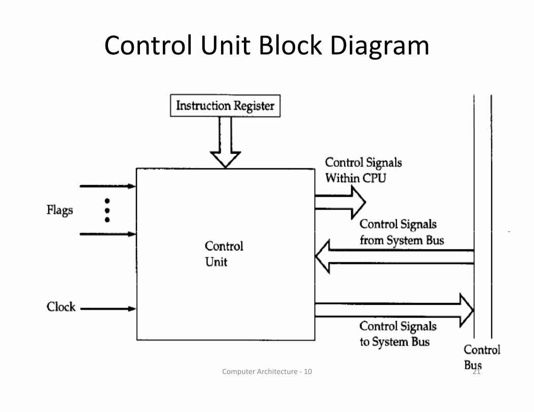
Control Unit Block Diagram
2Computer Architecture ‐ 10
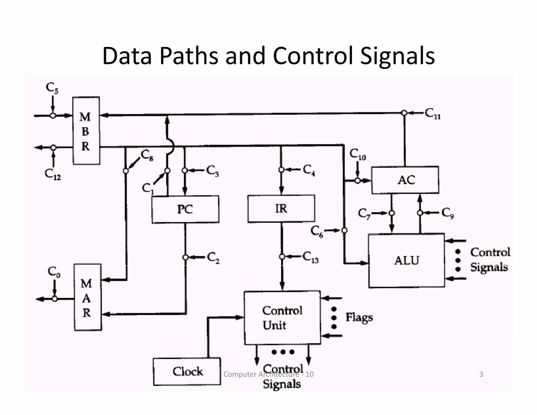
Data Paths and Control Signals
3Computer Architecture ‐ 10
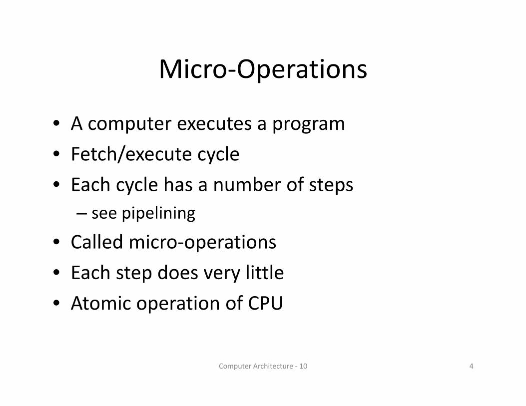
Micro‐OperationsMicro Operations
• A computer executes a programA computer executes a program
• Fetch/execute cycle
h l h b f• Each cycle has a number of steps– see pipelining
• Called micro‐operations
• Each step does very littlep y
• Atomic operation of CPU
4Computer Architecture ‐ 10
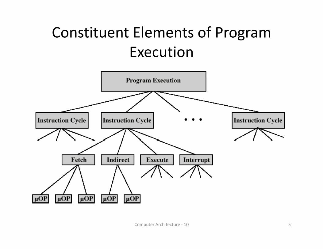
Constituent Elements of Program Execution
5Computer Architecture ‐ 10

Fetch ‐ 4 RegistersFetch 4 Registers
• Memory Address Register (MAR) – Connected to address bus
– Specifies address for read or write op
• Memory Buffer Register (MBR)• Memory Buffer Register (MBR) – Connected to data bus
– Holds data to write or last data read
• Program Counter (PC) – Holds address of next instruction to be fetched
• Instruction Register (IR)• Instruction Register (IR) – Holds last instruction fetched
6Computer Architecture ‐ 10
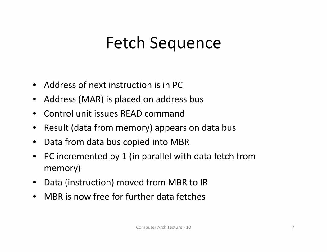
Fetch SequenceFetch Sequence
• Address of next instruction is in PC
• Address (MAR) is placed on address bus
l i i d• Control unit issues READ command
• Result (data from memory) appears on data bus
• Data from data bus copied into MBR• Data from data bus copied into MBR
• PC incremented by 1 (in parallel with data fetch from memory)
• Data (instruction) moved from MBR to IR
• MBR is now free for further data fetches
7Computer Architecture ‐ 10

Fetch Sequence (symbolic)Fetch Sequence (symbolic)
• t1: MAR < (PC)• t1: MAR <‐ (PC)• t2: MBR <‐ (memory)• PC <‐ (PC) +1• t3: IR <‐ (MBR)• (tx = time unit/clock cycle)• or• t1: MAR <‐ (PC)• t2: MBR <‐ (memory)( y)• t3: PC <‐ (PC) +1 • IR <‐ (MBR)
8Computer Architecture ‐ 10
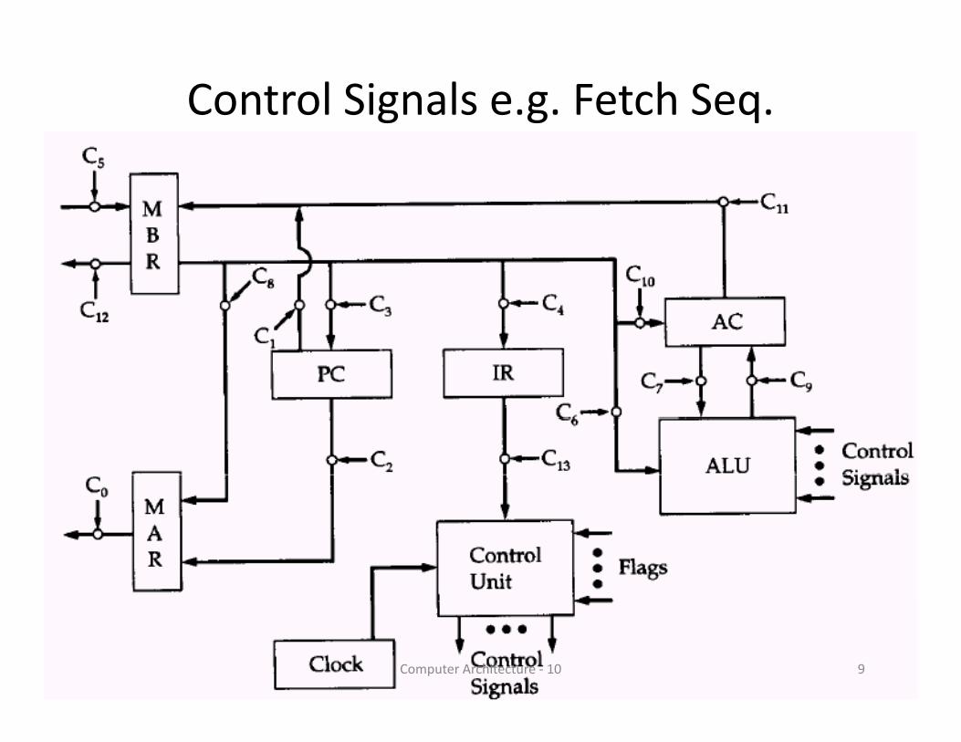
Control Signals e.g. Fetch Seq.
9Computer Architecture ‐ 10
Rules for Clock Cycle GroupingRules for Clock Cycle Grouping
P b f ll d• Proper sequence must be followed– MAR <‐ (PC) must precede MBR <‐ (memory)
C fli t t b id d• Conflicts must be avoided– Must not read & write same register at same time– MBR < (memory) & IR < (MBR) must not be in same– MBR <‐ (memory) & IR <‐ (MBR) must not be in same cycle
• Also: PC <‐ (PC) +1 involves addition( )– Use ALU– May need additional micro‐operations
10Computer Architecture ‐ 10
Indirect CycleIndirect Cycle
• MAR <‐ (IR dd ) ‐ address field of IRMAR < (IRaddress) address field of IR
• MBR <‐ (memory)
( )• IRaddress <‐ (MBRaddress)
• MBR contains an address
• IR is now in same state as if direct addressing ghad been used
• (What does this say about IR size?)(What does this say about IR size?)
11Computer Architecture ‐ 10
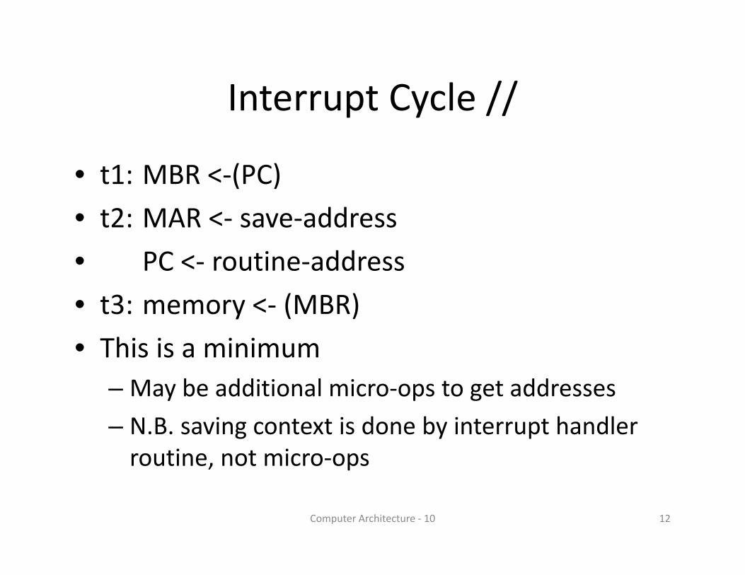
Interrupt Cycle //Interrupt Cycle //
• t1: MBR <‐(PC)t1: MBR < (PC)
• t2: MAR <‐ save‐address
C i dd• PC <‐ routine‐address
• t3: memory <‐ (MBR)
• This is a minimum– May be additional micro‐ops to get addressesay be add o a c o ops o ge add esses
– N.B. saving context is done by interrupt handler routine, not micro‐ops, p
12Computer Architecture ‐ 10
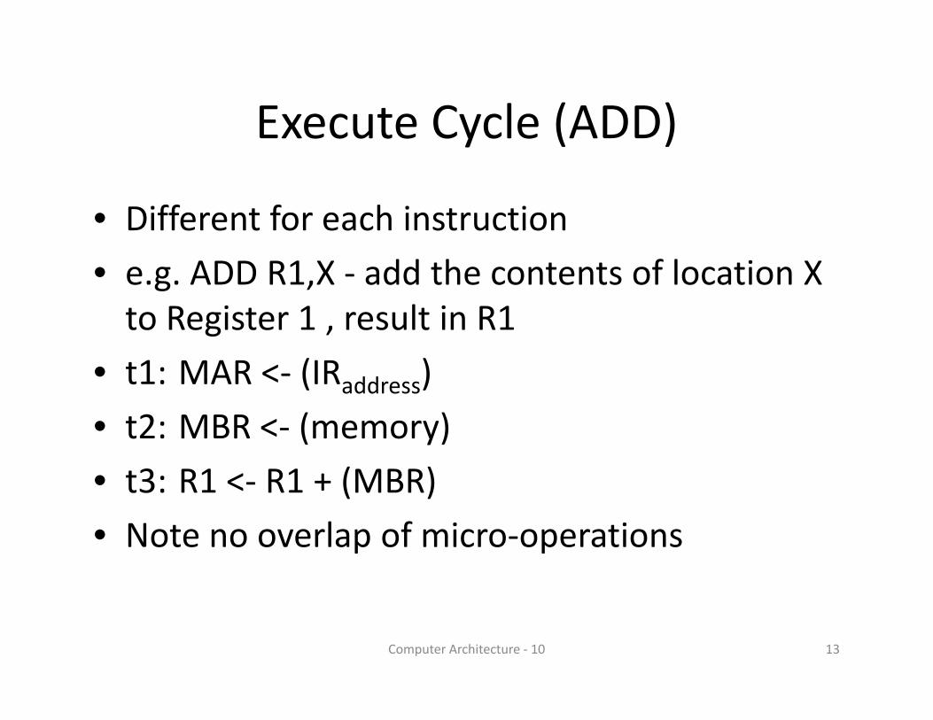
Execute Cycle (ADD)Execute Cycle (ADD)
• Different for each instructionDifferent for each instruction
• e.g. ADD R1,X ‐ add the contents of location X to Register 1 result in R1to Register 1 , result in R1
• t1: MAR <‐ (IRaddress)
• t2: MBR <‐ (memory)
• t3: R1 <‐ R1 + (MBR)( )
• Note no overlap of micro‐operations
13Computer Architecture ‐ 10

Data Paths and Control Signals
14Computer Architecture ‐ 10
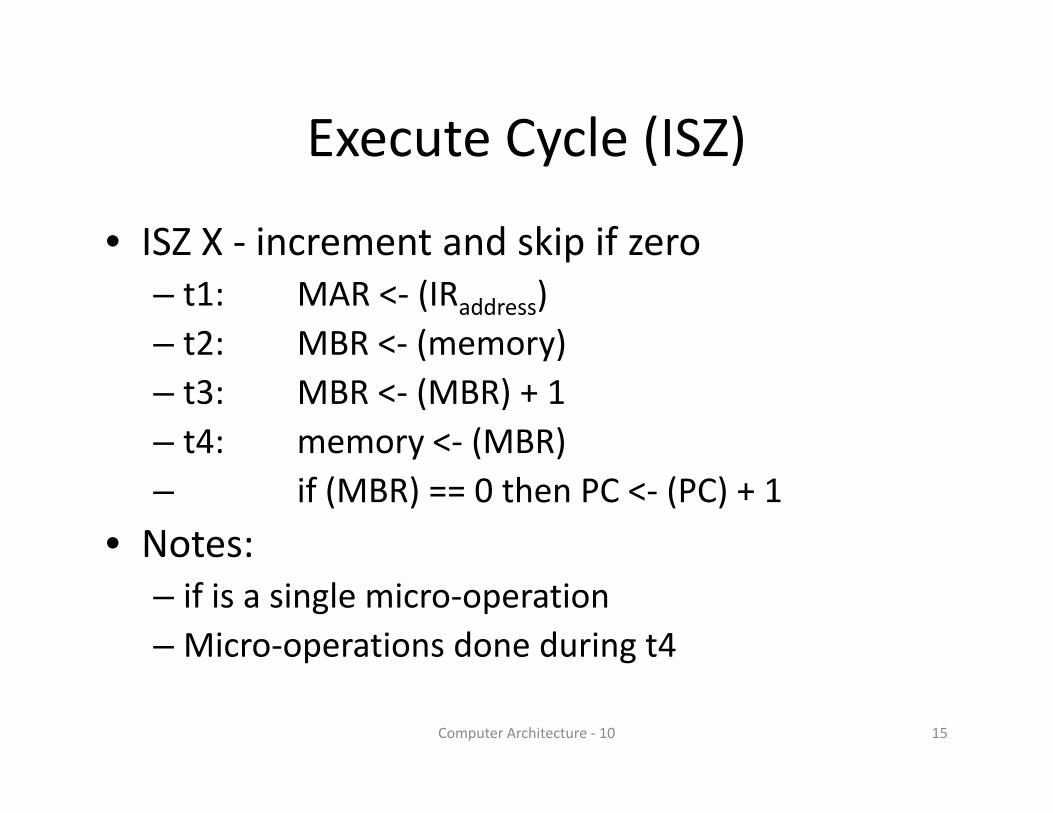
Execute Cycle (ISZ)Execute Cycle (ISZ)
• ISZ X ‐ increment and skip if zeroISZ X increment and skip if zero– t1: MAR <‐ (IRaddress)– t2: MBR <‐ (memory)( y)– t3: MBR <‐ (MBR) + 1– t4: memory <‐ (MBR)y ( )– if (MBR) == 0 then PC <‐ (PC) + 1
• Notes:– if is a single micro‐operation– Micro‐operations done during t4p g
15Computer Architecture ‐ 10
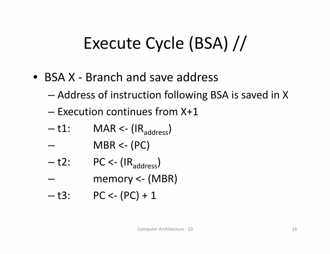
Execute Cycle (BSA) //Execute Cycle (BSA) //
• BSA X ‐ Branch and save addressBSA X Branch and save address– Address of instruction following BSA is saved in X
Execution continues from X+1– Execution continues from X+1
– t1: MAR <‐ (IRaddress)
MBR < (PC)– MBR <‐ (PC)
– t2: PC <‐ (IRaddress)
(MBR)– memory <‐ (MBR)
– t3: PC <‐ (PC) + 1
16Computer Architecture ‐ 10
Functional Requirements //Functional Requirements //
• Define basic elements of processorDefine basic elements of processor
• Describe micro‐operations processor performs
i f i l i• Determine functions control unit must perform
17Computer Architecture ‐ 10
Basic Elements of ProcessorBasic Elements of Processor
• ALUALU
• Registers
l d h• Internal data paths
• External data paths
• Control Unit
18Computer Architecture ‐ 10
Types of Micro‐operationTypes of Micro operation
• Transfer data between registersTransfer data between registers
• Transfer data from register to external
f d f l i• Transfer data from external to register
• Perform arithmetic or logical ops
19Computer Architecture ‐ 10
Functions of Control UnitFunctions of Control Unit
• SequencingSequencing– Causing the CPU to step through a series of micro‐operationsoperations
• ExecutionCausing the performance of each micro op– Causing the performance of each micro‐op
• This is done using Control Signals
20Computer Architecture ‐ 10
Control Unit Block Diagram
21Computer Architecture ‐ 10
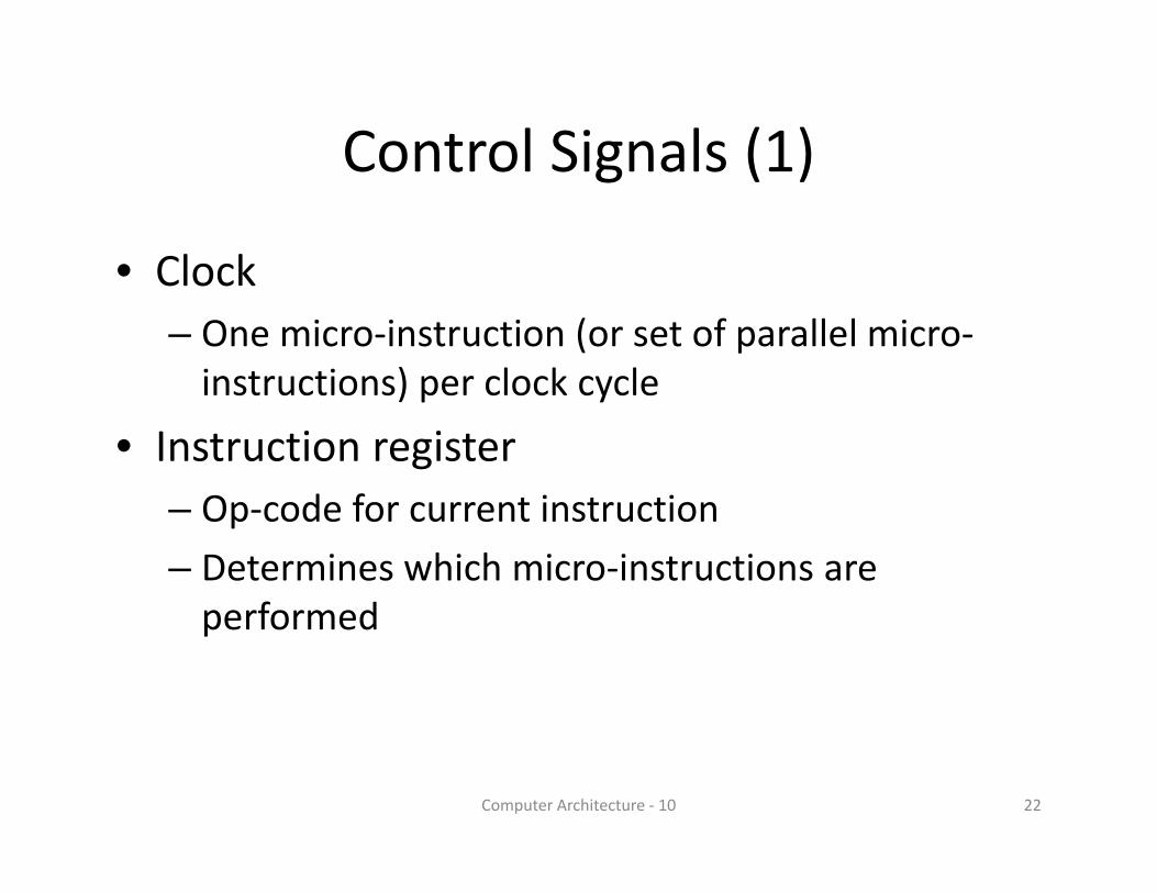
Control Signals (1)Control Signals (1)
• ClockClock– One micro‐instruction (or set of parallel micro‐instructions) per clock cycleinstructions) per clock cycle
• Instruction registerOp code for current instruction– Op‐code for current instruction
– Determines which micro‐instructions are performedperformed
22Computer Architecture ‐ 10
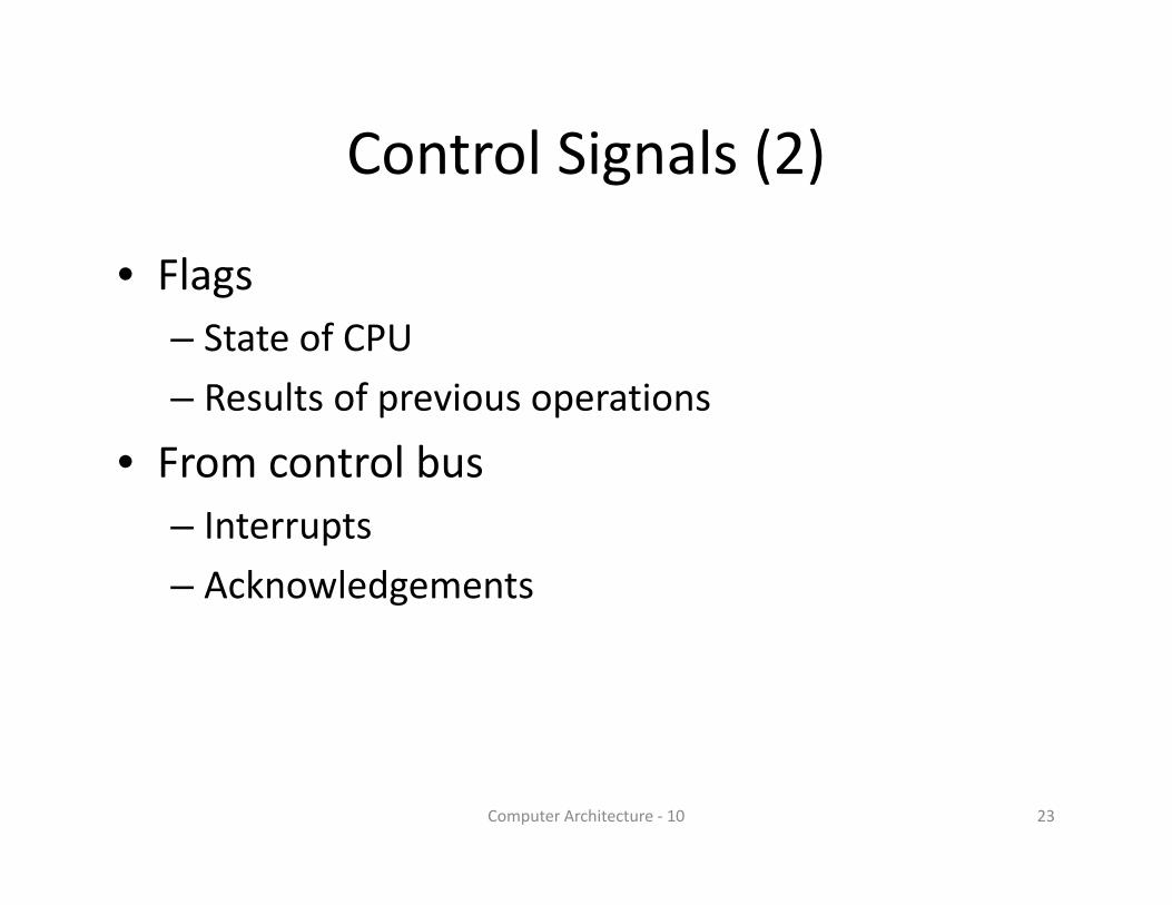
Control Signals (2)Control Signals (2)
• FlagsFlags– State of CPU
Results of previous operations– Results of previous operations
• From control bus– Interrupts
– Acknowledgements
23Computer Architecture ‐ 10
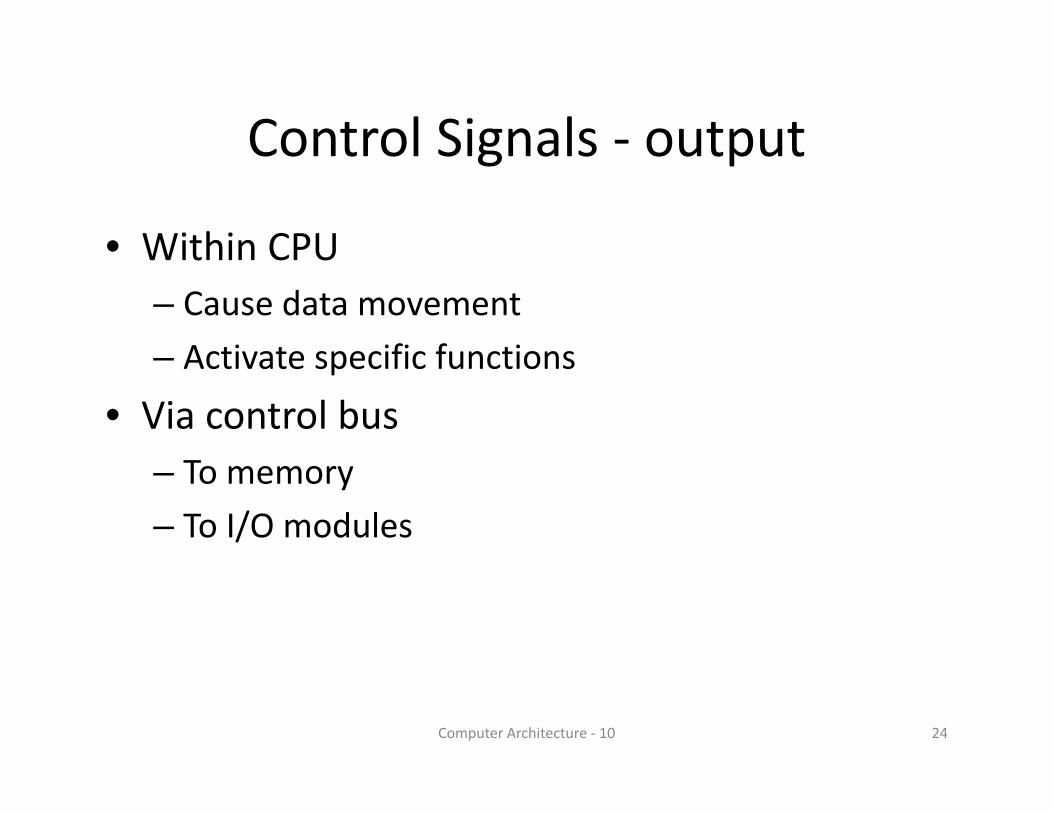
Control Signals ‐ outputControl Signals output
• Within CPUWithin CPU– Cause data movement
Activate specific functions– Activate specific functions
• Via control bus– To memory
– To I/O modules
24Computer Architecture ‐ 10
Example Control Signal Sequence ‐ Fetch
• MAR <‐ (PC)MAR < (PC)– Control unit activates signal to open gates between PC and MARbetween PC and MAR
• MBR <‐ (memory)Open gates between MAR and address bus– Open gates between MAR and address bus
– Memory read control signal
O t b t d t b d MBR– Open gates between data bus and MBR
25Computer Architecture ‐ 10
Internal OrganizationInternal Organization
• Usually a single internal busUsually a single internal bus
• Gates control movement of data onto and off the busthe bus
• Control signals control data transfer to and f l bfrom external systems bus
• Temporary registers needed for proper operation of ALU
26Computer Architecture ‐ 10
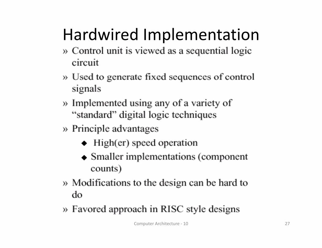
Hardwired Implementation
27Computer Architecture ‐ 10
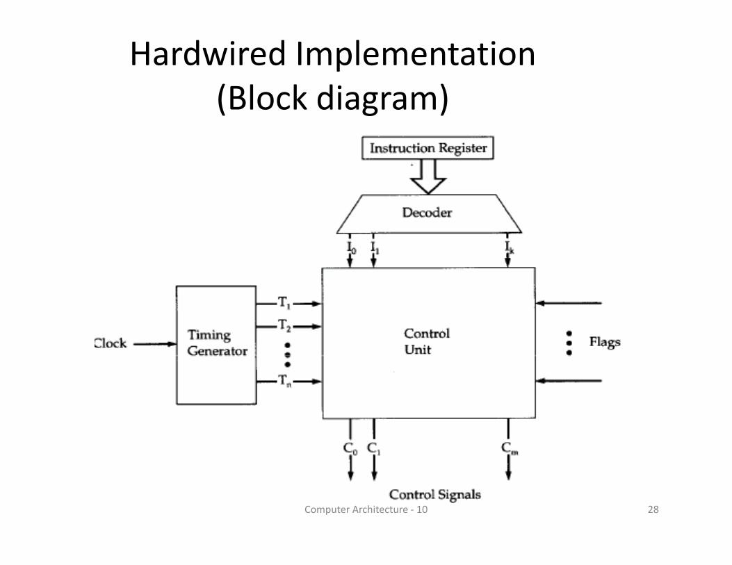
Hardwired Implementation (Block diagram)(Block diagram)
28Computer Architecture ‐ 10
Hardwired Implementation (1)Hardwired Implementation (1)
• Control unit inputsp• Flags and control bus
– Each bit means something• Instruction register
– Op‐code causes different control signals for each diff t i t tidifferent instruction
– Unique logic for each op‐code– Decoder takes encoded input and produces singleDecoder takes encoded input and produces single output
– n binary inputs and 2n outputs
29Computer Architecture ‐ 10
Hardwired Implementation (2)Hardwired Implementation (2)
• ClockClock– Repetitive sequence of pulses
Useful for measuring duration of micro ops– Useful for measuring duration of micro‐ops
– Must be long enough to allow signal propagation
Diff t t l i l t diff t ti ithi– Different control signals at different times within instruction cycle
Need a counter with different control signals for– Need a counter with different control signals for t1, t2 etc.
30Computer Architecture ‐ 10
Problems With Hard Wired DesignsProblems With Hard Wired Designs
• Complex sequencing & micro‐operation logicComplex sequencing & micro operation logic
• Difficult to design and test
fl ibl d i• Inflexible design
• Difficult to add new instructions
31Computer Architecture ‐ 10

QuestionsQuestions
32Computer Architecture ‐ 10


