Hier wird Wissen Wirklichkeit Computer Architecture – Part 3 – page 1 of 55 – Prof. Dr. Uwe Brinkschulte, M.Sc. Benjamin Betting Part 3 Fundamentals in Computer Architecture Computer Architecture Slide Sets WS 2013/2014 Prof. Dr. Uwe Brinkschulte M.Sc. Benjamin Betting
Transcript
Hier wird Wissen Wirklichkeit Computer Architecture – Part 3 – page 1 of 55 – Prof. Dr. Uwe Brinkschulte, M.Sc. Benjamin Betting
Part 3 Fundamentals in Computer Architecture
Computer Architecture
Slide Sets
WS 2013/2014
Prof. Dr. Uwe Brinkschulte M.Sc. Benjamin Betting
Hier wird Wissen Wirklichkeit Computer Architecture – Part 3 – page 2 of 55 – Prof. Dr. Uwe Brinkschulte, M.Sc. Benjamin Betting
Basic definitions
Computer Architecture defines the behavior and the attributes of a computer as seen by the programmer and user, no internal structural or organization details
Computer Organization the internal organization (datapaths, memory structures, input/output structures, e.g.) of a computer
Hier wird Wissen Wirklichkeit Computer Architecture – Part 3 – page 3 of 55 – Prof. Dr. Uwe Brinkschulte, M.Sc. Benjamin Betting
Basic definitions
Processor Architecture part of Computer Architecture, defines the view of the processor visible to the programmer or compiler developer, interface between hard- and software, no implementation details
Microarchitecture defines the concrete implementation of a processor architecture, several implementations of the same processor architecture might exist (e.g. Intel IA32)
Operation Principle defines the way the processor processes instructions and data
Hier wird Wissen Wirklichkeit Computer Architecture – Part 3 – page 4 of 55 – Prof. Dr. Uwe Brinkschulte, M.Sc. Benjamin Betting
Basic definitions
Hardware
Software
Computer Architecture
Processor
Operation Principle
Processor Architecture
Computer Organization
Memory
Input/ Output
Microarchitecture
Hier wird Wissen Wirklichkeit Computer Architecture – Part 3 – page 5 of 55 – Prof. Dr. Uwe Brinkschulte, M.Sc. Benjamin Betting
Basic definitions
Instruction Set defines the set of instructions executable by the given processor architecture
Instruction Set Architecture often used as a synonym to processor (ISA) architecture
Instruction Format defines the way operands are accessed by instructions,
instructions usually are divided into an opcode (tells what to do) and one ore more operands (tells on what to apply the opcode)
Hier wird Wissen Wirklichkeit Computer Architecture – Part 3 – page 6 of 55 – Prof. Dr. Uwe Brinkschulte, M.Sc. Benjamin Betting
Basic instruction formats
3-Address-Format Opcode, Dest, Src1, Src2
e.g. add C, B, A (C = A + B)
2-Address-Format Opcode, Dest/Src1, Src2
e.g. add B, A (B = A + B)
1-Address-Format Opcode, Src
e.g. add B (Accu = Accu + B)
a special accumulator register (Accu) is used
0-Address-Format Opcode
e.g. push A (C = A + B) push B add pop C Stack based architecture
Hier wird Wissen Wirklichkeit Computer Architecture – Part 3 – page 7 of 55 – Prof. Dr. Uwe Brinkschulte, M.Sc. Benjamin Betting
More basic definitions
Central Processing Unit central unit of a computer, (CPU, Processor) controls all computer operations consists of a control unit and a functional unit
control unit functional unit (datapath)
results
Instructions (command) operands (data)
The operation principle of a processor can be a sequential or a parallel processing of instructions (the program) The processing in one or more functional units is controlled by the control unit.
Hier wird Wissen Wirklichkeit Computer Architecture – Part 3 – page 8 of 55 – Prof. Dr. Uwe Brinkschulte, M.Sc. Benjamin Betting
More basic definitions
Microprocessor a CPU on a single chip
Microprocessor-System a technical system containing at least one microprocessor (may not be a computer, e.g. a phone)
Microcomputer a computer build from one or more micropressors, contains also memory, input/output (IO) and a connection system (bus)
Microcomputer-System a microcomputer with attached peripherals (e.g. keyboard, screen, mouse, printer, etc.)
Hier wird Wissen Wirklichkeit Computer Architecture – Part 3 – page 9 of 55 – Prof. Dr. Uwe Brinkschulte, M.Sc. Benjamin Betting
Microcomputer-System
Microcomputer
Microprocessor, CPU
More basic definitions
control unit functional unit (datapath)
memory (program, data) input/output
connection (bus)
peripherals
Hier wird Wissen Wirklichkeit Computer Architecture – Part 3 – page 10 of 55 – Prof. Dr. Uwe Brinkschulte, M.Sc. Benjamin Betting
More basic definitions
Memory consists of a linear set of memory cells
memory cells mostly have uniform size (e.g. a byte)
memory cells are identified by an address
Input/Output interface to the peripherals
like memory, IO units are identified by an address
. . .
address data
memory
. . .
address data
IO
Hier wird Wissen Wirklichkeit Computer Architecture – Part 3 – page 11 of 55 – Prof. Dr. Uwe Brinkschulte, M.Sc. Benjamin Betting
More basic definitions
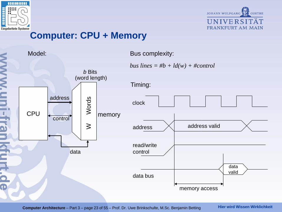
Bus connection system between CPU, memory and IO unit
Data Bus part of the bus where data (instructions or operands) is transfered (usually bidirectional)
Address Bus part of the bus where address information (memory or IO addresses) is transfered (usual unidirectional)
Control Bus part of the bus where control and status signals are transferred (partly unidirectional, partly bidirectional)
Data Bus
Address Bus
Control Bus
Bus
CPU side memory/IO side
Hier wird Wissen Wirklichkeit Computer Architecture – Part 3 – page 12 of 55 – Prof. Dr. Uwe Brinkschulte, M.Sc. Benjamin Betting
• The operation principle of a Von-Neumann-architecture defines that instructions are processed sequentially.
• Instructions and data are stored in the same main memory
• The opcode is to be applied to the operands.
• Depending on the opcode, the operands are interpreted as data or memory addresses of data.
• In the latter case, the instruction is applied to the content of the addressed memory cell.
The Von-Neumann-Architecture
Hier wird Wissen Wirklichkeit Computer Architecture – Part 3 – page 13 of 55 – Prof. Dr. Uwe Brinkschulte, M.Sc. Benjamin Betting
• An operand may also be interpreted as a jump pointer to an instruction.
• Since instructions and data reside in the same memory, a memory address may contain a data value or an instruction.
• Interpretation of a memory cell’s content depends on the opcode of the instruction only.
CPU address
data code
main memory
The Von-Neumann-Architecture
Hier wird Wissen Wirklichkeit Computer Architecture – Part 3 – page 14 of 55 – Prof. Dr. Uwe Brinkschulte, M.Sc. Benjamin Betting
The Von-Neumann-Architecture
control unit datapath
cond
ition
co
des
mic
ro
com
man
ds
processor ad
dres
ses
of d
ata
or c
omm
ands
control signals
data and instructions
program and data memory
Shared memory for program and data, sequential access. Von-Neumann-Architecture: • simple structure (only one memory) • program and data must access the memory one after another
Hier wird Wissen Wirklichkeit Computer Architecture – Part 3 – page 15 of 55 – Prof. Dr. Uwe Brinkschulte, M.Sc. Benjamin Betting
Operation Principle of Von-Neumann-Architecture Demonstration
control unit main memory
functional unit (datapath)
instruction address
instruction operand address
operand result address
result
Von-Neumann bottleneck!
data
address
control
decode execute
Hier wird Wissen Wirklichkeit Computer Architecture – Part 3 – page 16 of 55 – Prof. Dr. Uwe Brinkschulte, M.Sc. Benjamin Betting
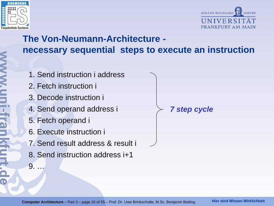
1. Send instruction i address 2. Fetch instruction i 3. Decode instruction i 4. Send operand address i 5. Fetch operand i 6. Execute instruction i 7. Send result address & result i 8. Send instruction address i+1 9. …
The Von-Neumann-Architecture - necessary sequential steps to execute an instruction
7 step cycle
Hier wird Wissen Wirklichkeit Computer Architecture – Part 3 – page 17 of 55 – Prof. Dr. Uwe Brinkschulte, M.Sc. Benjamin Betting
The Harvard-Architecture
The processor is augmented by a program memory which stores the program to be executed. Data is stored in a second memory, the data memory. Harvard-Architecture: • complex structure (two memories) • program and data can access their memories at the same time
function unit (data path)
(data register, ALU, shifter, MUX, DEMUX)
control unit
(program counter, instruction register,
control register)
condition codes
micro instructions
data memory
program memory
results
operands
control signals
instructions
control signals
instruction address
processor
Hier wird Wissen Wirklichkeit Computer Architecture – Part 3 – page 18 of 55 – Prof. Dr. Uwe Brinkschulte, M.Sc. Benjamin Betting
data memory
Operation Principle of Havard-Architecture Demonstration
control unit program memory
functional unit (datapath)
instruction address
instruction operand address
operand result result address
instruction instruction address
decode execute decode
data
address
control
Hier wird Wissen Wirklichkeit Computer Architecture – Part 3 – page 19 of 55 – Prof. Dr. Uwe Brinkschulte, M.Sc. Benjamin Betting
1. Send instruction i address 2. Fetch instruction i 3. Decode instruction i 4. Send operand address i 5. Fetch operand i | send instruction i+1 address 6. Execute instruction i | fetch instruction i+1 7. Send result address & result i | decode instruction i+1 8. Send operand address i+1 9. Fetch operand i+1 | send instruction i+2 address 10. Execute instruction i+1 | fetch instruction i+2 11. Send result address & result i+1 | decode instruction i+2 12. …
The Havard-Architecture - necessary sequential steps to execute an instruction
4 step cycle
i
i+1
overlap
Hier wird Wissen Wirklichkeit Computer Architecture – Part 3 – page 20 of 55 – Prof. Dr. Uwe Brinkschulte, M.Sc. Benjamin Betting
• The microprocessor receives the instructions in sequential order from the main memory. Therefore, the control unit contains a program counter (PC) to address the instructions
• It decodes each instruction and executes an operation on the content of the memory cell addressed by the instruction.
• In Von-Neumann-Architecture, the interpretation of the memory cell’s content (data or instruction) depends only on the information in the instruction. Data and instructions are stored in the main memory in the same way and are indistinguishable from memory side therefore .
• The memory cells themselves don’t keep track of the type of their content.
• The only structuring is the size of the smallest addressable unit given by the bit width (8, 16, 32, or 64).
Hier wird Wissen Wirklichkeit Computer Architecture – Part 3 – page 21 of 55 – Prof. Dr. Uwe Brinkschulte, M.Sc. Benjamin Betting
The computer executes three phases which may overlap:
• In the instruction retrieval phase the content of a memory cell which is addressed by the program counter is fetched.
• In the decode phase the content of the retrieved memory cell is interpreted as an instruction.
• In the execution phase the contents of one or two memory cells are fetched and processed depending on the command given by the opcode. It is thereby assumed that the memory cells contain data which are conform to the given preconditions.
Hier wird Wissen Wirklichkeit Computer Architecture – Part 3 – page 22 of 55 – Prof. Dr. Uwe Brinkschulte, M.Sc. Benjamin Betting
Decode: case IR is when add: nextstate <= Execute_add1; when sub: nextstate <= Execute_sub1; when load: nextstate<= Execute_load1; when store: nextstate <= Execute_store1: end case;
......
Instruction cycle based on FSMD model
Hier wird Wissen Wirklichkeit Computer Architecture – Part 3 – page 27 of 55 – Prof. Dr. Uwe Brinkschulte, M.Sc. Benjamin Betting
• To execute an instruction, it is loaded into the instruction register IR and decoded. The decoding is done by the FSM control unit (CU).
• Decoding the instruction yields the control signals for the arithmetic logic units (ALU) in the datapath.
• It furthermore selects up to three register – two for reading and one for writing (three-ported register file).
• It also provides the write enable signals for the write operations
• The ALU combines two operands, which are taken from the register file or from the instruction itself.
Hier wird Wissen Wirklichkeit Computer Architecture – Part 3 – page 28 of 55 – Prof. Dr. Uwe Brinkschulte, M.Sc. Benjamin Betting
• In case of a LOAD instruction, the ALU calculates the effective address. Then, the contents of the addressed memory cell is loaded into the register file.
• On a STORE-Instruction the calculation of the effective address is also necessary. The operand to store must be made available at the same time.
• Furthermore, the ALU generates flags (CC: condition codes), which can be evaluated by the control unit.
• The program counter (PC) holds the address of the instruction to be executed next. It is normally incremented automatically (+).
Hier wird Wissen Wirklichkeit Computer Architecture – Part 3 – page 29 of 55 – Prof. Dr. Uwe Brinkschulte, M.Sc. Benjamin Betting
Instruction cycle of an existing sequential processor in pseudocode
1: forever {
2: npc = pc + 1
3: instr = prog [pc]
4: opcode 5: a = data [source addr1] 6: b = data [source addr2]
7: d = dest addr
8: case (opcode) { 9: ADD: data [d] = a + b 10: SUB: data [d] = a - b 11: : 12: BEQ: if (a == b) npc = d 13: : 14: }
15: pc = npc
16: }
data memory
instruc -tion
memory PC
ALU
instruction decoder
+1
Hier wird Wissen Wirklichkeit Computer Architecture – Part 3 – page 30 of 55 – Prof. Dr. Uwe Brinkschulte, M.Sc. Benjamin Betting
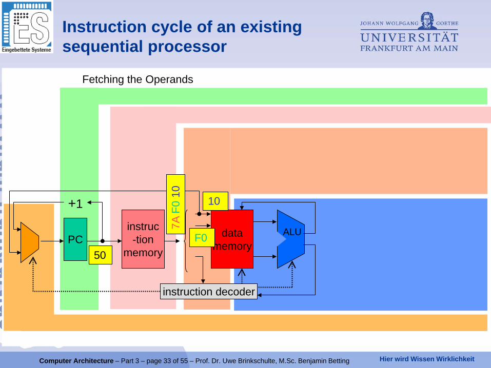
Executing a sample instruction:
• Add content of data memory at address 10 to content of data memory at address F0, store the result at address 10 (2-address format)
• Instruction in fictive assembler mnemonics: ADD (F0),(10)
• Instruction in fictive machine code: 7A F0 10
• Instruction address in instruction memory: 50
• Content of data memory at address 10: 05
• Content of data memory at address F0: 02
Instruction cycle of an existing sequential processor
Hier wird Wissen Wirklichkeit Computer Architecture – Part 3 – page 31 of 55 – Prof. Dr. Uwe Brinkschulte, M.Sc. Benjamin Betting
Instruction cycle of an existing sequential processor
data memory
instruc -tion
memory PC
ALU
instruction decoder
+1
50
Fetching the Instruction
Hier wird Wissen Wirklichkeit Computer Architecture – Part 3 – page 32 of 55 – Prof. Dr. Uwe Brinkschulte, M.Sc. Benjamin Betting
Instruction cycle of an existing sequential processor
data memory
instruc -tion
memory PC
ALU
instruction decoder
+1
Decoding the Instruction
7A F
0 10
50
Hier wird Wissen Wirklichkeit Computer Architecture – Part 3 – page 33 of 55 – Prof. Dr. Uwe Brinkschulte, M.Sc. Benjamin Betting
Instruction cycle of an existing sequential processor
data memory
instruc -tion
memory PC
ALU
instruction decoder
+1
Fetching the Operands
50 F0
10
7A F
0 10
Hier wird Wissen Wirklichkeit Computer Architecture – Part 3 – page 34 of 55 – Prof. Dr. Uwe Brinkschulte, M.Sc. Benjamin Betting
Instruction cycle of an existing sequential processor
data memory
instruc -tion
memory PC
ALU
instruction decoder
+1
Executing the Instruction
50 F0
10 05
02 7A
7A F
0 10
Hier wird Wissen Wirklichkeit Computer Architecture – Part 3 – page 35 of 55 – Prof. Dr. Uwe Brinkschulte, M.Sc. Benjamin Betting
Instruction cycle of an existing sequential processor
data memory
instruc -tion
memory PC
ALU
instruction decoder
+1
Storing the Result
50 F0
10 05
02 7A
07 7A
F0
10
Hier wird Wissen Wirklichkeit Computer Architecture – Part 3 – page 36 of 55 – Prof. Dr. Uwe Brinkschulte, M.Sc. Benjamin Betting
Instruction cycle of an existing sequential processor
data memory
instruc -tion
memory PC
ALU
instruction decoder
+1
Incrementing the PC
50
51
Hier wird Wissen Wirklichkeit Computer Architecture – Part 3 – page 37 of 55 – Prof. Dr. Uwe Brinkschulte, M.Sc. Benjamin Betting
Multiplexer based 3 address Load-Store architecture for a CPU
Hier wird Wissen Wirklichkeit Computer Architecture – Part 3 – page 38 of 55 – Prof. Dr. Uwe Brinkschulte, M.Sc. Benjamin Betting
• The hardware cost of the Von-Neumann-principle is minimal.
• It had its value in times when the hardware components were the biggest cost factor of a computer and optimal memory utilization was the most important design goal.
• However, in the last three decades the cost situation has changed fundamentally due to the development of semiconductor technology.
• As shown, particularly the connection between main memory and processor proves to be a bottleneck, as all data and instructions have to be transported by it.
Hier wird Wissen Wirklichkeit Computer Architecture – Part 3 – page 39 of 55 – Prof. Dr. Uwe Brinkschulte, M.Sc. Benjamin Betting
• Today, the processor’s instruction execution is significantly faster than the memory access, which even worsens the situation.
• Processor techniques like instruction pipelining, superscalar principle, multithreading and multicores increased the data requirements considerably.
Therefore, the pure Von-Neumann-Architecture principle is dropped in modern microprocessors.
Cache-based Harvard-Architectures in combination with time and spatial parallelism can be found
Hier wird Wissen Wirklichkeit Computer Architecture – Part 3 – page 40 of 55 – Prof. Dr. Uwe Brinkschulte, M.Sc. Benjamin Betting
As seen, an instruction cycle consists of the part cycles: 1. instruction fetch 2. decode 3. instruction execute. In each instruction cycle at most one instruction is fetched from the main memory and then executed. This results in a sequential control flow.
This computer class is called SISD: Single Instruction Single Data
Classifications
Hier wird Wissen Wirklichkeit Computer Architecture – Part 3 – page 41 of 55 – Prof. Dr. Uwe Brinkschulte, M.Sc. Benjamin Betting
SISD Single Instruction Single Data Von-Neumann SIMD Single Instruction Multiple Data Array- or Vectorprocessors, Multimedia Extensions MISD Multiple Instruction Single Data Fault-Tolerance (controversial) MIMD Multiple Instruction Multiple Data GRID, Cloud, Multicore, Supercomputers
Flynn Classification
Hier wird Wissen Wirklichkeit Computer Architecture – Part 3 – page 42 of 55 – Prof. Dr. Uwe Brinkschulte, M.Sc. Benjamin Betting
There are basically two possible structures for the control unit: • direct (hardwired) control • micro programmed control
The hardwired solution is mainly used in RISC designs whereas microprogramming is more common among CISC.
The hardwired solution uses a FSM consisting of a hardwired combinatorial circuit to decode the instructions. This requires simple and regular instructions such as it is given by a RISC-ISA.
Complex instructions, which are common in CISC, are interpreted using a micro programmed control.
Classification by Control Unit
Hier wird Wissen Wirklichkeit Computer Architecture – Part 3 – page 43 of 55 – Prof. Dr. Uwe Brinkschulte, M.Sc. Benjamin Betting
Hardwired control
hardwired control
data
control signals
state register
complex combinatorial network
instruction register (IR) opcode; addr. etc.
ALU
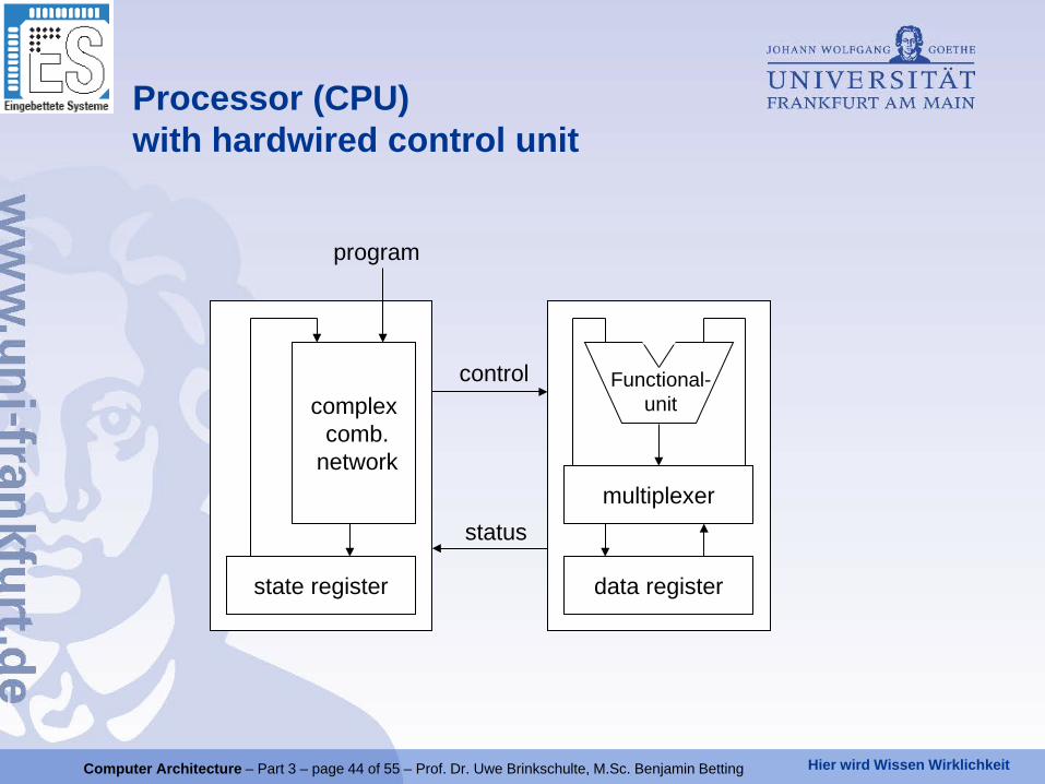
Hier wird Wissen Wirklichkeit Computer Architecture – Part 3 – page 44 of 55 – Prof. Dr. Uwe Brinkschulte, M.Sc. Benjamin Betting
Processor (CPU) with hardwired control unit
state register data register
multiplexer
Functional- unit complex
comb. network
program
status
control
Hier wird Wissen Wirklichkeit Computer Architecture – Part 3 – page 45 of 55 – Prof. Dr. Uwe Brinkschulte, M.Sc. Benjamin Betting
register
Implementation of a microprogrammed FSM
Dec
oder
clock
bit lines
word lines
next state vector
control vector
xt
zt
yt
yt+1 zt+1
Hier wird Wissen Wirklichkeit Computer Architecture – Part 3 – page 46 of 55 – Prof. Dr. Uwe Brinkschulte, M.Sc. Benjamin Betting
Adding the datapath to the microprogrammed FSM
decoder microprogram memory
state register C ALU
control register C
ALU result
next address
Instruction (program)
operands
control path data path
Hier wird Wissen Wirklichkeit Computer Architecture – Part 3 – page 47 of 55 – Prof. Dr. Uwe Brinkschulte, M.Sc. Benjamin Betting
Adding a sequencer to allow more comfortable microprogram operations
decoder microprogram memory
sequencer control C ALU
control register C
ALU result
Instruction (program)
operands
control path data path
Sequencer, µP counter
Hier wird Wissen Wirklichkeit Computer Architecture – Part 3 – page 48 of 55 – Prof. Dr. Uwe Brinkschulte, M.Sc. Benjamin Betting
Microprogrammed control data bus
control signals
address part control part
instruction
microprogram
sequencer opcode addr. etc.
micro instruction counter micro program memory micro instruction register
start address
mapping ROM D
instruction register
(micro) status information from ALU (FLAG)
µBZ
µPS
µIR
Hier wird Wissen Wirklichkeit Computer Architecture – Part 3 – page 49 of 55 – Prof. Dr. Uwe Brinkschulte, M.Sc. Benjamin Betting
Processor (CPU) with micro programmed control unit
state register data register
multiplexer
Functional- unit
Micro program
Sequencer
program
status
control
Hier wird Wissen Wirklichkeit Computer Architecture – Part 3 – page 50 of 55 – Prof. Dr. Uwe Brinkschulte, M.Sc. Benjamin Betting
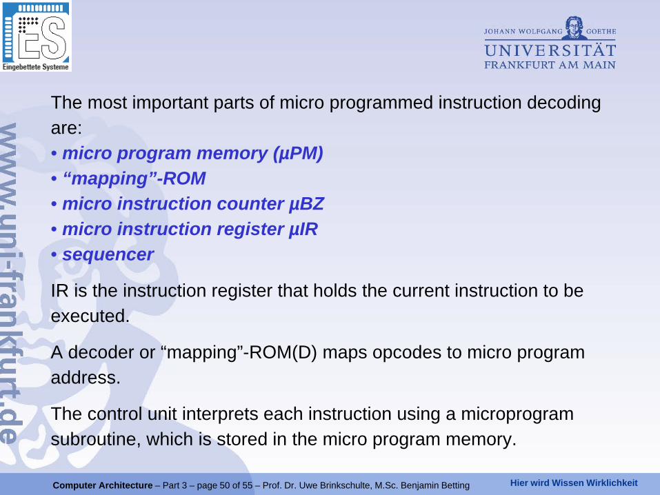
The most important parts of micro programmed instruction decoding are: • micro program memory (µPM) • “mapping”-ROM • micro instruction counter µBZ • micro instruction register µIR • sequencer
IR is the instruction register that holds the current instruction to be executed.
A decoder or “mapping”-ROM(D) maps opcodes to micro program address.
The control unit interprets each instruction using a microprogram subroutine, which is stored in the micro program memory.
Hier wird Wissen Wirklichkeit Computer Architecture – Part 3 – page 51 of 55 – Prof. Dr. Uwe Brinkschulte, M.Sc. Benjamin Betting
A microprogram consists of a series of discrete microprogram instructions (micro instructions). When an instruction is executed, the sequence of micro instructions, whose start address is determined from the opcode, is processed.
The start address is loaded into the µBZ. The addressed micro instruction is loaded into the micro instruction register.
The micro program sequencer determines the address of the next micro instruction according to the control and address codes of the current one as well as the status flags of the ALU.
This micro instruction is loaded into the micro instruction register.
Selecting the next micro instruction and controlling the data path is done in parallel.
Hier wird Wissen Wirklichkeit Computer Architecture – Part 3 – page 52 of 55 – Prof. Dr. Uwe Brinkschulte, M.Sc. Benjamin Betting
microprogram memory
Horizontal microprogramming is characterized by a direct mapping of the bits of the micro instruction onto the control signals (micro order).
register
. . .
ALU control
sequencer control
bus control
fully parallel
Hier wird Wissen Wirklichkeit Computer Architecture – Part 3 – page 53 of 55 – Prof. Dr. Uwe Brinkschulte, M.Sc. Benjamin Betting
Quasi-horizontal microprogramming differs therein that each micro instruction is grouped in bit fields, which have to be decoded.
These fields may hold the address of the next micro instruction, the micro order for the ALU, numbers of registers or control signals for multiplexers. The associated decoders are usually part of the data path. The width of a microprogram word is shrinked while parallelism is reduced
microprogram memory
. . .
ALU control
sequencer control
bus control
register
decoder field select
partly parallel
Hier wird Wissen Wirklichkeit Computer Architecture – Part 3 – page 54 of 55 – Prof. Dr. Uwe Brinkschulte, M.Sc. Benjamin Betting
If the micro instructions are being decoded using firmware, this is called nanoprogramming.
microprogram memory
. . .
ALU control
sequencer control
bus control
register
field select
nanoprogram memory
register
partly sequential
Hier wird Wissen Wirklichkeit Computer Architecture – Part 3 – page 55 of 55 – Prof. Dr. Uwe Brinkschulte, M.Sc. Benjamin Betting
• The number of separate paths for instructions and operands (Von- Neumann and Harvard architecture respectively)
• The instruction set architecture (CISC/RISC)
• The location, where operands are placed for processing:
- memory-memory machine: The operands are loaded directly from the main memory. Fast registers as buffers for operands are abandoned.
- virtual-register machine: A part of the main memory is used like a register file.
- register-register or load/store machine: The operands have to be placed in registers before processing. This kind of architecture is going to be described in detail in the following.