UNIVERSITY OF PENNSYLVANIA Conducting Nanofilaments in Metal Oxide Resistive Switching Memory Qualifying Exam Manuscript Yang Lu Department of Material Science and Engineering 6 May, 2013 Contact Email: [email protected]
Chemical and structural properties ofconducting nanofilaments inTiN/HfO2-based resistive switchingstructuresP Calka, E Martinez, V Delaye, D Lafond, G Audoit, D Mariolle,N Chevalier, H Grampeix, C Cagli, V Jousseaume and C Guedj
CEA, LETI, MINATEC Campus, 17 rue des Martyrs, 38054 Grenoble Cedex 9, France
Received 10 September 2012, in final form 21 December 2012Published 5 February 2013Online at stacks.iop.org/Nano/24/085706
AbstractStructural, chemical and electronic properties of electroforming in the TiN/HfO2 system areinvestigated at the nanometre scale. Reversible resistive switching is achieved by biasing themetal oxide using conductive atomic force microscopy. An original method is implemented tolocalize and investigate the conductive region by combining focused ion beam, scanningspreading resistance microscopy and scanning transmission electron microscopy. Resultsclearly show the presence of a conductive filament extending over 20 nm. Its size and shape ismainly tuned by the corresponding HfO2 crystalline grain. Oxygen vacancies together withlocalized states in the HfO2 band gap are highlighted by electron energy loss spectroscopy.Oxygen depletion is seen mainly in the central part of the conductive filament along grainboundaries. This is associated with partial amorphization, in particular at both electrode/oxideinterfaces. Our results are a direct confirmation of the filamentary conduction mechanism,showing that oxygen content modulation at the nanometre scale plays a major role in resistiveswitching.
(Some figures may appear in colour only in the online journal)
1. Introduction
Resistive random access memories (RRAM) are promisingcandidates for the next generation of non-volatile memories.They are of potential interest to achieve high integrationdensity, high speed of operation and low power consump-tion [1, 2]. The RRAM consists of a metal–insulator–metal(MIM) structure that exhibits a reversible change of resistanceunder biasing. At a specific threshold voltage, known as theforming voltage, the resistance evolves from the pristine highresistive state (HRS) to a low resistive state (LRS). Duringthis so-called electroforming step, a soft dielectric breakdownis assumed to occur and resistive switching is activated. Acurrent limitation is enforced to reduce damage in the MIMstructure and avoid permanent dielectric breakdown. Succes-sive alternating switching cycles (>106) between both LRS
and HRS states can then be performed, these may be eitherunipolar and bipolar depending on whether the switchingdirection depends on the polarity of the applied voltage.
The resistive switching phenomenon has been observedin a wide variety of materials, such as the transition metaloxides (NiO [3], TiO2 [4], TaOx [5], WOx [6], ZrO2 [7]).Among these, HfO2 has attracted much attention [8–11]because it offers low fabrication costs and good compatibilitywith the conventional metal oxide semiconductor field effecttransistors (MOSFETs) fabrication process. However, theswitching mechanism is still not fully understood. It isbelieved that an active region is formed in a confinedarea between the top and bottom electrodes, the so-calledconductive filament (CF) [1, 2]. To improve our knowledgeof the physical mechanism involved in resistive switching,a direct observation of this conductive filament is required,
but this is challenging. Indeed, the conductive region isthought to be unique and randomly located between theelectrodes, thus making its localization and observationvery difficult. Resistive switching has been achieved usingconductive atomic force microscopy (C-AFM) [12–16],offering the possibility to analyse individual conductivefilaments. Recently, direct observations of conductive regionshave been made on NiO [17, 18], TiO2 [19] and Ta2O5 [20],but regarding HfO2, nothing has been reported yet in theliterature to our knowledge.
In this study, a specific protocol has been implementedto address this issue. Conductive regions are created in HfO2and then localized to investigate the structural and chemicalproperties after the electroforming process. We focus here onthis first critical step, which defines both the CF properties andthe switching characteristics of resistive memories. Workingwithout a permanent top electrode allows easier localizationof the conductive path. The oxide is locally switched at thenanometre scale with an AFM nanoprobe (top electrode). Theconductive region is then localized by scanning spreadingresistance microscopy (SSRM). A direct observation is madeby scanning transmission electron microscopy (STEM) toinvestigate the chemical and electronic changes involved inthe switching mechanism. Significant results are obtainedregarding the properties of the conductive filaments. Answersregarding the chemical composition, crystallinity, electronicstructure and morphology are obtained at the nanometre scale.Our results are in agreement with the filamentary conductionmechanism based on the segregation of oxygen vacancies.This is, to our knowledge, the first experimental evidence ofsuch conducting nanofilaments in HfO2-based structures.
2. Experiment
A 20 nm thick TiN layer is sputtered on top of a Si(100)wafer covered by a thin (2 nm) native SiO2 film. De-oxidationof the TiN surface is done by chemical etching (HF1%) before deposition of a 10 nm thick HfO2 layer byatomic layer deposition (ALD) at 350 ◦C using HfCl4 andH2O. Both the TiN electrode and HfO2 oxide have apolycrystalline structure, as already reported elsewhere [21].The stoichiometry of the pristine HfO2 oxide is measuredby Rutherford back-scattering spectroscopy (RBS). The O/Hfratio is found to be 2.3, with an uncertainty of 5%, showingthat the initial oxide is presumably oxygen rich, probablybecause of residual –OH groups due to the H2O-based ALDgrowth.
A specific protocol in five steps has been developedin order to produce and localize a conductive region inthe TiN/HfO2 system. A partial cross-section (CS) is firstprepared by focused ion beam (FIB) using a gallium beamin a dual beam Helios system from FEI. Two parallel trenches(1 × 10 µm2) of approximately 2 nm depth are designed onboth sides of a pristine HfO2 area (1× 10 µm2). The depth iskept very low to preserve the electrical contact of the bottomTiN electrode. Resistive switching is then performed in thisdelimited area to facilitate further localization and observationof the conductive area.
Resistive switching is performed using AFM D3100equipment from Bruker in the conducting mode (C-AFM).The sample is previously heated at 120 ◦C for 12 hunder atmospheric pressure to remove moisture and surfacecontamination. Measurements are then performed in a glovebox with a constant N2 flux, i.e. with reduced humidity(<2% of H2O). These two precautions are taken to minimizewater dissociation and subsequent detrimental effects such asoxide regrowth [22], leading to an increase of the formingvoltage, or injection of charged species (OH−,H+), leading toparasitic leakage currents [23]. Highly doped diamond coatedSi tips from Nanosensors are used (Rtip = 5–8 k�). The tipradius is in the range 20–50 nm, depending of the shape ofthe diamond grain at the tip apex. The tip force is set in the0.1–0.5 µN range to ensure efficient electrical contact andlow mechanical pressure (<0.5 GPa). The resulting possibledamage is thus assumed to be rather weak. The TiN bottomelectrode is grounded whereas the tip is biased using an HP4155A parameter analyser. Resistive switching is performedwith the tip held at a fixed location while the voltage isswept. The current flowing through the oxide lies in the range10−14–10−3 A.
In order to localize the conductive region afterresistive switching, topography and conductivity maps aresimultaneously acquired in contact mode by SSRM on thecross-section. A positive voltage (1 V), which is below the set(Vset) and forming (Vforming) voltages, is applied to the TiNlayer while the tip is grounded. The resistance is measuredwithin the detection limits, from 104 to 1010 �. To enable adirect observation of the conductive region by STEM, the finalcross-section is prepared by FIB. Protective coatings (SiOCHand Pt) are deposited on top of the HfO2 partial CS beforethe lift-out. The lamella is prepared by thinning this section athigh energy (30 keV), with a final cleaning step performedat low energy (5 keV) to minimize surface amorphizationeffects.
Finally, the chemical composition of the conductiveregion is studied by electron energy loss spectroscopy(EELS) using the Cs probe and image corrected TitanUltimate Microscope from FEI, equipped with a QuantumGatan energy filter and a scanning module. STEM–EELSmeasurements are carried out with an acceleration voltageof 200 keV. Elemental maps are estimated by measuringthe absorption edge area, after a power law backgroundsubtraction. Edge area densities (at× cts nm−2) are estimatedusing the formula NITotal = Ik/σk, where N is the atomicconcentration, and Ik and σk are respectively the intensity andionization cross-section of the absorption edge. A chemicalsensitivity of 0.1 at.% is achieved. STEM–EELS chemicalmaps are recorded with an energy resolution of 1.6 eV anda spatial resolution of 0.5 nm. The relative lamella thicknesst/λ is calculated using the formula t/λ = ln(ITotal/IElastic),where ITotal and IElastic are respectively the intensity of thewhole spectrum and zero-loss peak, λ is the electron inelasticmean free path and t is the lamella thickness [24]. Additionalinformation about the structure and composition of the activeregion is obtained with Z-contrast imaging using a high-angleannular dark-field detector (HAADF) and high-resolutiontransmission electron microscopy (HR-TEM).
2
Nanotechnology 24 (2013) 085706 P Calka et al
Figure 1. (a) Experimental setup used for resistive switching of the TiN/HfO2 stack with a polarized conductive AFM diamond coated Sitip as a top electrode. (b) Corresponding electrical schematics. (c) I(Va) characteristics measured by biasing the AFM tip (Va = 4 V).(d) I(Ve) characteristics obtained by taking into account the tip resistance and effective voltage Ve seen by the TiN/HfO2 stack.
3. Results and discussion
3.1. Electrical properties of the TiN/HfO2 system
First, the resistive switching properties of the TiN/HfO2system are tested using the blanket Si/SiO2/TiN/HfO2sample. C-AFM measurements are performed by applying theanalyser voltage (Va ∼ 4 V) directly on the AFM conductivetip. The experimental setup and the corresponding equivalentelectrical circuit are displayed in figures 1(a) and (b). The tipresistance (Rtip) affects the electroforming process, especiallywhen high current densities flow through the oxide. Apotential drop is expected over the AFM tip, thus decreasingthe effective voltage (Ve) applied to the TiN/HfO2 stack. Notethat Rtip is in the 5–8 k� range, i.e. 2–3 orders of magnitudehigher than for a conventional metallic electrode.
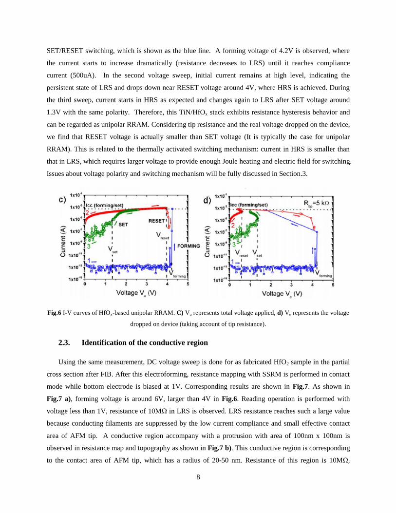
Several successive voltage sweeps are performed in theunipolar mode by biasing the tip with positive voltages(figure 1(c)). During the first voltage sweep, the initial currentintensity flowing through the oxide is around 10 fA. At thethreshold voltage of 4.2 V (Vforming), the current intensityincreases dramatically. During this electroforming process,the insulating oxide evolves into a conductive state (LRS).The compliance current Icc is set at 500 µA to reduce damageinduced by high current densities flowing through the stack.During the second voltage sweep, the initial current (∼2 µA)indicates that the conductive state is persistent. The oxideis thus stabilized in the LRS state. When increasing thevoltage, the current intensity reaches the mA range, sinceno compliance current is applied. At a threshold voltage of3.9 V (Vreset), a drop of the current is observed (3 orders ofmagnitude). This is the so-called reset process, bringing the
oxide into a high resistive state (HRS). During the third sweep,the oxide resistance changes again from HRS to LRS. This isthe set process, occurring at a voltage of 1.3 V (Vset). For thesame reason as for the electroforming process, the compliancecurrent is also activated.
After taking into account the tip resistance, assumed tobe the same for the electroforming, reset and set processesand equal to 5 k�, the resulting I(Ve) curves are plotted infigure 1(d). The shape of the curves is modified only forhigh current densities, where the tip resistance correctioninduces a decrease of the effective voltage (Ve). The newthreshold voltages are measured with the methodologydescribed in a previous work [11]. Vforming and Vset are notaffected by the tip resistance, whereas Vreset decreases, thusleading to the expected behaviour regarding the unipolarswitching mode [25] (Vset higher than Vreset). Note thatfor quantitative measurements of the film conductivity, forinstance the resistance ratio between LRS and HRS states, aSchottky barrier effect should be considered at the tip/oxideinterface [26], which might introduce a significant resistanceand modify the Vreset voltage as well.
These results show that the TiN/HfO2/diamond (AFMtip) stack exhibits unipolar resistive switching. The resistancechange is reversible and successive set/reset processes can beactivated at the same bias polarity. The current intensity andforming voltage measured for the reset process are similar tothat of our integrated devices [27].
3.2. Electroforming and identification of the conductivefilament
Following the same C-AFM protocol, resistive switching isnow performed on the pristine HfO2 area contained in the
3
Nanotechnology 24 (2013) 085706 P Calka et al
Figure 2. (a) I(Ve) characteristics of the electroforming (bluesquares) and reading (red circles) steps performed on the HfO2partial cross-section with the conductive AFM tip before lift-out ofthe TEM lamella. Inset: SEM image of the HfO2 surface after theelectroforming/reading electrical stresses. (b) Topography andresistance maps measured by SSRM on the switched HfO2.
partial CS prepared by FIB, as described in section 2. Thecorresponding I(Ve) characteristic is plotted in figure 2(a).Once again, a compliance current of 500 µA is appliedduring the electroforming process. A second bias voltagesweep (up to 1 V) is performed subsequently, confirming thestability of the LRS (red rings). In the inset of figure 2(a),the SEM (scanning electron microscopy) image shows a darkcontrast corresponding to the electrically stressed region.The SEM contrast is usually attributed to a change of thesurface topography or to charge trapping. Here, this contrastis presumably related to the conductive region.
To confirm this assumption and clearly identify thisarea as being highly conductive, a precise localization ofthe conductive region is done at the nanometre scale byresistance mapping with SSRM before thinning and lift-outof the cross-section. The surface is scanned in contact modewhen biasing the TiN bottom electrode (1 V). Topographyand resistance maps are simultaneously acquired. Both imagesare plotted in figure 2(b). A conductive area together witha small protrusion is observed and perfectly correlated onboth maps. This protrusion has a resistance of 107 � at 1 V,therefore the current in this conductive region is 10−7 A.This value is in good agreement with the current intensitymeasured for the LRS state (see figure 2(a)), showing that theSSRM measurement does not modify the conductive region.This was also checked on a pristine HfO2 area (not shown),since no modifications were observed after doing SSRMin the same conditions. The conductive area is round andextends over 100 nm at the HfO2 surface. However, this sizemight be overestimated because of the relatively high contactarea (∼100 nm) between the tip and the HfO2 surface. Toget a better insight of the size, shape and composition ofthis conductive region, and thus of the physical phenomena
Figure 3. STEM–HAADF image measured for the conductiveregion identified in figure 2(b).
involved in resistive switching, the partial cross-section islifted-out and thinned to allow direct observation by STEM.
Figure 3 shows the STEM–HAADF image measured inthe region of interest. All the layers of the Si/SiO2/TiN/HfO2stack are identified by Z-contrast imaging. The conductiveregion is clearly visible, corresponding to a protrusion 3 nmin height. As seen on this image, the morphology of the HfO2layer has changed, whereas the underlying layers, includingthe TiN bottom electrode, are not modified. Dark contrastis observed at the left side of the conductive region. This isa thickness-related contrast, due to FIB milling, which wasmore important in the left region, yielding a thinner lamella inthe left part. This assumption is confirmed by the protectiveSiOCH and Pt being missing at the top of the lamella.
3.3. Chemical properties of the conductive filament
STEM–EELS measurements are performed in the protrudingregion mentioned in section 3.2 and displayed in the HAADFimage of figure 4(a). Oxygen, nitrogen and titanium maps,acquired by measuring the O–K (532 eV), N–K (401 eV)and Ti–L2,3 (456 eV) edges, are displayed in figures 4(b)–(d).These elemental maps are derived from the integration of thefull edges (532–560 eV for O, 396–421 eV for N, 456–481 eVfor Ti). In the oxygen map (see figure 4(b)), only the SiOCHand HfO2 layers exhibit high oxygen content, as expected.As discussed before, we again observe a thickness-relatedcontrast along the cross-section, corresponding to dark andbright blue contrasts on the left and right sides of the HfO2layer, respectively. Nevertheless, a localized oxygen-deficientregion (dark contrast inside the red circle) is highlighted inthe protruding HfO2 area. This region seems mainly localizedat the top of the HfO2 layer, with an extension of 20 nm inthe lateral direction. Ti and N maps show that no diffusion ofmetallic atoms from the bottom electrode is observed insidethe oxide. Furthermore, there is no migration from the topelectrode material (diamond coated silicon tip) or from carbonsurface contamination in the HfO2 layer, as confirmed by Cand Si maps (not shown).
Further information is obtained by a detailed analysisof the conductive region. Oxygen and thickness profiles areplotted in the horizontal direction, along the oxygen-deficient
4
Nanotechnology 24 (2013) 085706 P Calka et al
Figure 4. (a) STEM–HAADF image of the conductive region:zoom on the HfO2 layer. (b)–(d) STEM–EELS chemical maps ofthe conductive region: (b) oxygen map, (c) nitrogen map,(d) titanium map.
and oxygen-rich regions (see figure 5). A drop of the oxygenconcentration is clearly seen and related to a modification ofthe oxide after electroforming. The lamella thickness, alsoplotted in figure 5, is constant along the same profile (see redline in figure 5(b)). The oxygen drop is thus not correlated toa decrease of the lamella thickness, but really representativeof the electroforming. The oxygen loss is estimated to be ashigh as 55%± 15% in some points. We thus demonstrate herethat the electroforming step creates an oxygen-poor regionin the Hf oxide, labelled as HfO2−x conductive region inthe rest of the paper. Our results clearly show that oxygencontent modulation at the nanometre scale plays a major rolein resistive switching of HfO2-based structures.
3.4. Electronic properties of the conductive filament
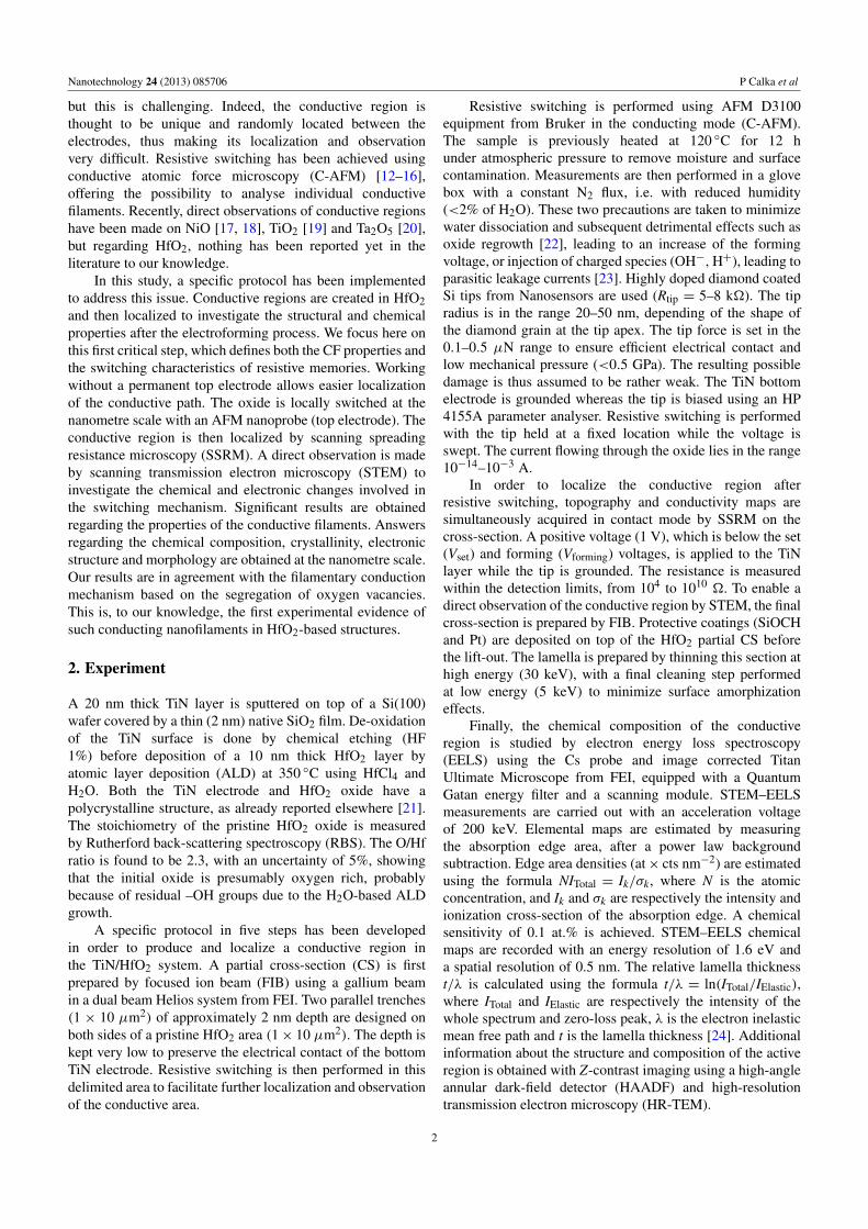
Additional information about the electronic properties of theHfO2−x conductive region is obtained by a detailed analysisof the oxygen K-edge (532 eV) EELS spectra measuredat each pixel of the oxygen map. Spectra extracted in theoxygen-deficient (HfO2−x) and oxygen-rich (HfO2) regionsare plotted in figure 6(a).
The reference spectrum, extracted from the oxygen-richregion, is characterized by the typical double peak structure(contributions I and II at 536 and 539 eV), already observedfor crystalline HfO2 [28]. These near-edge fine structuresare attributed to the excitation of a O 1s core level electroninto an unoccupied state in the conduction band of HfO2,mainly composed by cation Hf 5d states [29]. The oxygenK-edge spectrum is explained by an hybridization of Hf 5dand O 2p states, since the s→ d transition is forbidden by
Figure 5. (a) Zoom on the oxygen-deficient region in HfO2corresponding to the red circle of figure 4. (b) Oxygen concentrationand relative thickness (t/λ) of the lamella, plotted along the dashedline of figure 5(a).
the dipole selection rule [30]. The two main peaks are relatedto the so-called crystal-field splitting via this Hf 5d/O 2phybridization. Indeed, energy splitting of Hf 5d orbitals isknown to form the eg and t2g sub-bands [31, 32] because of theelectrostatic field created by the oxygen atoms around each Hfatom.
Significant differences are observed for the oxygenK-edge measured in the HfO2−x conductive region. First, adecrease of the intensity of the global spectrum is observedand presumably related to the reduced number of oxygenatoms in this region. Second, the shape is modified, withthe occurrence of a shoulder (III) at the low-energy sideof component I, which is worth noting although veryweak, together with an additional contribution (IV) betweencomponents I and II. The shoulder on the low-energyside of component I could be related to the creation ofoxygen vacancies which induce localized states [25, 33]within the band gap of HfO2. This feature has already beenobserved by Baik et al [33] at HfO2 grain boundaries, knownto be oxygen deficient and confirmed by first-principlescalculations including O vacancies in HfO2 supercells [33].This additional structure is explained by the excitation ofa O 1s core level electron into localized states within theband gap. This transition requires less energy than a transitioninto the conduction band. Thus, this structure appears shiftedtowards lower energies. The additional contribution (IV) isalso probably related to oxygen vacancies. Similarities can bemade with Wilk’s results [28], showing that the gap between
5
Nanotechnology 24 (2013) 085706 P Calka et al
Figure 6. (a) EELS oxygen K-edges spectra of the oxygen-rich(HfO2) and oxygen-poor (HfO2−x) regions acquired in STEMmode. (b) EELS oxygen K-edges spectra measured in the TiNbottom electrode and SiOCH upper layer. All the measurements aredone in regions where the lamella thickness is the same (see blacksquares on figure 7).
peaks I and II is filled for as-deposited HfO2 compared toannealed samples, i. e. with increasing oxygen vacancies andthus differing oxygen coordination around metal Hf ions. Thistrend has also been reported by Ostanin et al [34] when dopingzirconia with trivalent yttrium (YSZ for yttria-stabilizedzirconia), which introduces oxygen vacancies for chargeneutrality reasons. Additional structures are seen to appear inbetween components I and II for calculated ELNES spectraof such materials [35]. Note that, in our case, this additionalstructure is not attributed to electron beam damage, as shownby the spectrum measured for the oxygen-rich region, whichis not influenced by such a process. Finally, the initial doublepeak structure also evolves for the oxygen-deficient region.Indeed, the width and separation of peaks I and II aredifferent and might also be related to oxygen vacancies. Thebroadening of these structures has already been observed byStemmer et al [29] for amorphous Hf1−xAlxOy oxides andassigned to local atomic disorder. In our case, the expectedmovement of oxygen atoms probably induces such localdisorder as well as changes in the point defect chemistry. Theenergy difference between components I and II is also knownto vary with the material composition [36] and in particularwith oxygen loss in our case. This is confirmed by Ostanin’sresults [34, 35], reporting a shift of the second peak (II)
Figure 7. Images of the a–d coefficients used to model the oxygenK-edges EELS spectra measured at each pixel of the STEM–EELSchemical maps. Reference spectra for each compound (HfO2,HfO2−x, TiN and SiOCH) were extracted from regions marked bysmall black squares.
towards higher energies when increasing the concentration ofO vacancies in YSZ.
The near-edge fine structures of the oxygen K-edge areused to obtain information about the chemical and electronicproperties of the conductive region at the nanometre scale.EELS spectra measured at each pixel of the oxygen map (seefigure 4) are modelled using the minimum linear least squares(MLLS) routine of the Gatan digital micrograph software.Reference oxygen K-edge spectra are extracted from theoxygen-rich (HfO2) and oxygen-poor (HfO2−x) regions (seefigure 6(a)) as well as from the neighbouring TiN and SiOCHlayers (see figure 6(b)). No oxygen edge is measured for thebottom TiN electrode, confirming the absence of an interfacialTiON layer. The oxygen K-edge measured for SiOCH has asingle peak at higher energies (540 eV). A linear combinationof these spectra is used to reproduce the O K-edge (SO–K)
measured at each pixel of the O map, following the equation:
SO–K = aSO–K(HfO2)+ bSO–K(HfO2−x)
+ cSO–K(SiOCH)+ dSO–K(TiN) (1)
where SO–K(HfO2), SO–K(HfOx), SO–K(SiOCH), andSO–K(TiN) are the reference oxygen K-edges spectra. Theresulting images are plotted in figure 7 for the regionof interest. These coefficients highlight the location ofunoccupied electronic states into the conduction band for eachcompound (HfO2, HfO2−x, TiN and SiOCH).
The first two images (see figures 7(a) and (b)) arecomplementary and exhibit respectively low and highcontrasts in the conductive region. This result is consistentwith the existence of an oxygen-poor region, as discussed in
6
Nanotechnology 24 (2013) 085706 P Calka et al
Figure 8. (a) High-resolution TEM image of the HfO2−x conductive region. The grain boundaries are identified by dashed lines and theamorphous regions are labelled (A). (b) Fast Fourier transformed micrographs of selected areas (left HfO2 crystalline grain and amorphousarea labelled A2 of HfO2−x) of the high-resolution TEM image together with the corresponding simulated diffraction patterns formonoclinic HfO2.
section 3.3. The conductive region is characterized by a highdensity of defects such as oxygen vacancies, thus modifyingthe HfO2 electronic properties after the electroforming step.Oxygen vacancies are known to be related to localized stateswithin the HfO2 band gap. These intermediate band gapstates might favour electron conduction along the oxide,thus explaining the resistive switching. Figures 7(c) and(d) show the location of unoccupied states relative to theTiN and SiOCH oxygen K-edges. They are located ineach corresponding layer, thus confirming the absence ofinter-diffusion phenomena.
3.5. Structural properties of the conductive filament
When looking at the STEM–EELS oxygen map, the oxygenvacancies and thus the conductive region seem to be mainlylocated at the top of the HfO2 layer. More precise informationabout the CF location, shape and crystalline structure isobtained by HR-TEM. The image measured when zoomingon the conductive region is presented in figure 8(a). Theposition, dimension and shape of the main central grain aresimilar to the conductive region identified in sections 3.3 and3.4. This region is thus identified as an individual conductivefilament, which is not limited to the grain boundaries (seedashed lines) but extended over one specific grain 20 nmin size. This observation is in agreement with the resultsreported by Bersuker et al [37], indicating a spatial extensionof the leakage path at the deca-nanometre scale. This maincentral grain is characterized by a different crystallographicorientation compared to the left and right HfO2 grains. Thisis also the case for the TiN grain, which is perfectly alignedwith the CF. This particular configuration might favour thegrowth of the CF at this specific location. The properties ofthe CF are therefore probably strongly related to the structureof both materials and thus to the corresponding depositiontechniques. Fast Fourier transformed (FFT) micrographs
of selected areas of this HR-TEM image are presentedin figure 8(b) together with their corresponding simulateddiffractions patterns obtained using the JEMS software andassuming a HfO2 monoclinic structure. The FFT micrographextracted from the central part of the CF, labelled A2,highlights additional rings compared to the one extracted froma neighbouring HfO2 grain. This indicates partial localizedamorphization of the CF. Similar results are obtained for theregions labelled A1 and A3.
The CF is known to grow parallel to the electric fieldapplied between both electrodes and to be preferentiallycreated at the grain boundaries (GB), as stated by Lanzaet al [38]. Our results show that the CF is not fully extendedalong the vertical direction but some part is missing at thebottom side. This CF was probably initiated along the smallvertical grain boundary at the bottom side where the electricfield and conductivity is much higher. Our results support thehot electron injection model of Bersuker et al [37], whereelectrons are injected from the cathode into the oxide throughgrain boundaries. The intersection point between the threegrain boundaries seen on the HR-TEM image must have beena critical point to favour the spatial extension of the CFwhile growing along the oxide. At this point, the injectedelectrons start to create defects such as oxygen vacancies.This is confirmed when looking at figures 7(a) and (b),where we clearly see that most of the oxygen vacancies arecreated at this point and inside the main central grain. Oxygenions then probably migrate towards the anode under thehigh electric field. This conductive region remains crystallinedespite some local atomic disorder related to oxygen loss.This is confirmed by the diffraction patterns extracted fromselected areas of the CF, showing partial amorphization (seefigure 8(b)). On the central and bottom side (A2 and A3),amorphization is probably due to local heating and subsequentoxygen loss. The temperature must have increased drasticallybecause of the high current density flowing along the smallvertical grain boundary. On the top side (A1), the amorphous
7
Nanotechnology 24 (2013) 085706 P Calka et al
character as well as the deformation of the oxide layer isprobably related to the accumulation of oxygen. This isconsistent with the protrusion observed both by SSRM andSTEM–HAADF. This oxygen is assumed to come mainlyfrom the HfO2−x region, as oxygen migration towards theanode (AFM tip) is expected. However, we cannot rule outhere possible oxygen incorporation after resistive switchingduring air exposure between the SSRM and FIB preparationsteps and surface amorphization due to the AFM-inducedwear under mechanical and electrostatic forces.
3.6. Discussion
STEM–HAADF measurements show that a localized(∼20 nm) conductive region is created during the electroform-ing step induced by C-AFM in the TiN/HfO2 system. Analysisof the structural, chemical and electronic properties is doneat the nanometre scale by direct STEM–EELS observation.An oxygen-deficient region is identified, corresponding toa protrusion 3 nm in height with clear morphologicalchanges. Analysis of the near-edge fine structures observedon the EELS oxygen K-edge spectra highlights the presenceof oxygen vacancies. HR-TEM observations confirm thatelectroforming is a local phenomenon based on oxygenmigration, starting and propagating through grain boundariesand finally extending over a larger area.
Regarding the HfO2-based systems, the conductionmechanisms mentioned in the literature are mainly based onelectrical measurements [39–42]. Our work brings furtherinsights about the physico-chemical phenomena involved inresistive switching. Experimental proof of the major roleof oxygen is done thanks to direct observation of theconductive region. STEM–EELS results show the existenceof an oxygen-deficient region containing a high density ofoxygen vacancies and associated band gap states. This is adirect confirmation of the filamentary conduction mechanism,based on the breaking of Hf–O bonds and migration ofoxygen under high electric fields (>10 MV cm−1) andelevated temperatures. Doubly charged oxygen vacancies(V2+
o ) and oxygen interstitials ions (O2−i ) appear to be the
most energetically favourable point defects that can be createdin HfO2, as shown by ab initio calculations [43, 44]. Apossible physical interpretation of the switching mechanismis thus based on the creation of such defects, as described bythe following relationship:
HfO2 → HfO2−x + xV2+o + xO2−
i . (2)
Negatively charged interstitial oxygen ions are created and,near the vacancy, the resulting positive charge (2+) is locallytransferred to the metallic d states of the surrounding Hfatoms. Oxygen ions (O2−
i ) are driven towards the anode(positively biased AFM tip) under electrical stress. Theyprobably accumulate near the HfO2 surface yielding the3 nm high protrusion observed by SSRM and HR-TEM (seefigure 8). They might also oxidize near the anode (AFMtip) with charge transfer and oxygen desorption (2O2−
i →
O2 + 4e). However, the CF does not seem to protrude fromthe cathode, connecting both electrodes during electroforming
as a result of oxygen vacancies segregation. On the contrary,our results show that the conductive path is first generated byelectron injection along grain boundaries. Then, at a smalldistance from the cathode, a high concentration of oxygenvacancies is created (see figures 7(b) and 8). Subsequentgrowth of the CF is achieved in one particular grain bysegregation of oxygen vacancies when increasing the currentdensity and local temperature during the electroformingevent. The conductive region is thus characterized by itslocal character (∼20 nm) and high density of defects,such as oxygen vacancies acting as possible traps forelectron conduction through the oxide. Note that the CFproperties mentioned here are strongly correlated to thespecific conditions of the electroforming process in termsof effective voltage, current overshoot, and C-AFM protocol(tip composition and size, N2 atmosphere). In particular, theoxygen-poor environment used for resistive switching mightinduce field-assisted oxygen extraction, thus increasing theoxygen deficiency in the CF.
4. Conclusion
To conclude, reversible resistive switching of the TiN/HfO2
stack is performed using C-AFM. A precise identificationof the conductive region created during electroforming isachieved at the nanometre scale by SSRM. Direct Z-contrastimaging, STEM–EELS analysis and HR-TEM measurementsare made on this individual CF. Results clearly show thatthe conductive region extends over 20 nm and is still mainlycrystalline despite morphological changes and local atomicdisorder. This area appears to be oxygen deficient. EELSoxygen K-edges highlight the presence of oxygen vacanciesassociated with localized states in the HfO2 band gap.HR-TEM shows that generation and propagation of the CFis done along grain boundaries, where the electric field andconductivity is much higher. Partial amorphization is observedat both electrode/oxide interfaces due heating effects oroxygen accumulation. These results are a direct confirmationof the filamentary conduction mechanism, showing thatelectroforming is a local phenomenon related to a strongmodulation of the oxygen content. The process is mainlybased on the injection of electrons from the cathode, creationof oxygen vacancies in the oxide and movement of oxygenions towards the anode. These results contribute to a betterunderstanding of the switching mechanism in HfO2-basedOxRRAM structures for future device optimization.
Acknowledgments
All the measurements were performed at the CEA-LETINanoCharacterisation Centre (NCC) of Minatec. The authorsare grateful to the French ‘Recherche Technologique de Base’program for the measurements performed with the FEI TitanUltimate and to Amal Chabli and Francois Bertin for fruitfuldiscussions. This work was partially funded by the Frenchpublic authorities through the Nano2012 research program.
8
Nanotechnology 24 (2013) 085706 P Calka et al
References
[1] Sawa A 2008 Mater. Today 11 28[2] Waser R, Dittmann R, Staikov G and Szot K 2009 Adv. Mater.
21 2632[3] Baek I G et al 2004 Tech. Dig.—Int. Electron Devices Meet.
p 587[4] Kim S, Biju K P, Jo M, Jung S, Park J, Lee J, Lee W, Shin J,
Park S and Hwang H 2011 IEEE Electron Device Lett.32 671
[5] Lijie Z, Ru H, Minghao Z, Shiqiang Q, Yongbian K, Dejin G,Congyin S and Yangyuan W 2010 IEEE Electron DeviceLett. 31 966
[6] Chien W C et al 2010 IEEE Electron Device Lett. 31 126[7] Chih-Yang L, Chen-Yu W, Chung-Yi W, Tzyh-Cheang L,
Fu-Liang Y, Chenming H and Tseung-Yuen T 2007 IEEEElectron Device Lett. 28 366
[8] Gonon P, Mougenot M, Vallee C, Jorel C, Jousseaume V,Grampeix H and El Kamel F 2010 J. Appl. Phys.107 074507
[9] Walczyk D, Walczyk C, Schroeder T, Bertaud T, Sowinska M,Lukosius M, Fraschke M, Tillack B and Wenger C 2011Microelectron. Eng. 88 1133
[10] Yu-Sheng C, Heng-Yuan L, Pang-Shiu C, Tai-Yuan W,Ching-Chiun W, Pei-Jer T, Chen F, Ming-Jinn T andChenhsin L 2010 IEEE Electron Device Lett. 31 1473
[11] Jousseaume V et al 2011 Solid-State Electron. 58 62[12] Son J Y and Shin Y H 2008 Appl. Phys. Lett. 92 222106[13] Szot K, Speier W, Bihlmayer G and Waser R 2006 Nature
Mater. 5 312[14] Lee D, Seong D J, Jo I, Xiang F, Dong R, Oh S and
Hwang H 2007 Appl. Phys. Lett. 90 122104[15] Choi B J et al 2005 J. Appl. Phys. 98 033715[16] Son J Y, Kim D Y, Kim H, Maeng W J, Shin Y S and
Shin Y H 2011 Electrochem. Solid State Lett. 14 H311[17] Fujii T et al 2011 J. Appl. Phys. 109 053702[18] Uenuma M, Zheng B, Kawano K, Horita M, Ishikawa Y,
Yamashita I and Uraoka Y 2012 Appl. Phys. Lett.100 083105
[19] Kwon D H et al 2010 Nature Nanotechnol. 5 148[20] Wei Z et al 2011 Electron Devices Mtg (IEDM), 2011 IEEE
Jousseaume V, Bertin F and Guedj C 2011 Microelectron.Eng. 88 1142
[22] Arinero R, Hourani W, Touboul A D, Gautier B, Ramonda M,Albertini D, Militaru L, Gonzalez-Velo Y, Guasch C andSaigne F 2011 J. Appl. Phys. 110 014304
[23] Hourani W, Gautier B, Militaru L, Albertini D,Descamps-Mandine A and Arinero R 2011 Microelectron.Eng. 51 2097
[24] Egerton R F 2009 Rep. Prog. Phys. 72 25[25] Waser R and Aono M 2007 Nature Mater. 6 833[26] Lee M-H and Hwang C-S 2011 Nanoscale 3 490[27] Cagli C et al 2011 Electron Devices Mtg (IEDM), 2011 IEEE
Int. 28.7.1[28] Wilk G D and Muller D A 2003 Appl. Phys. Lett. 83 3984[29] Stemmer S, Chen Z Q, Zhu W J and Ma T P 2003 J. Microsc.
210 74[30] Egerton R F 1996 Electron Energy-Loss Spectroscopy in the
Electron Microscope (New York: Plenum)[31] Jang J H, Jung H S, Kim J H, Lee S Y, Hwang C S and
Kim M 2011 J. Appl. Phys. 109 023718[32] McComb D W 1996 Phys. Rev. B 54 7094[33] Baik H S, Kim M, Park G S, Song S A, Varela M,
Franceschetti A, Pantelides S T and Pennycook S J 2004Appl. Phys. Lett. 85 672
[34] Ostanin S, Craven A J, McComb D W, Vlachos D, Alavi A,Finnis M W and Paxton A T 2000 Phys. Rev. B 62 14728
[35] Ostanin S, Craven A J, McComb D W, Vlachos D, Alavi A,Paxton A T and Finnis M W 2002 Phys. Rev. B 65 224109
[36] Vlachos D, Craven A J and McComb D W 2001 J. Phys.:Condens. Matter 13 10799
[37] Bersuker G et al 2011 J. Appl. Phys. 110 124518[38] Lanza M, Zhang K, Porti M, Nafria M, Shen Z Y, Liu L F,
Kang J F, Gilmer D and Bersuker G 2012 Appl. Phys. Lett.100 123508
[39] Yu S, Jeyasingh R, Wu Y and Wong H S P 2012 Phys. Rev. B85 045324
[40] Yu S, Jeyasingh R, Wu Y and Wong H S P 2011 Appl. Phys.Lett. 99 232105
[41] Wong H S P, Lee H Y, Yu S, Chen Y S, Wu Y, Chen P S,Lee B, Chen F T and Tsai M J 2012 Proc. IEEE 100 1951
[42] Goux L, Czarnecki P, Chen Y Y, Pantisano L, Wang X P,Degraeve R, Govoreanu B, Jurczak M, Wouters D J andAltimime L 2010 Appl. Phys. Lett. 97 243509
[43] Zheng J X, Ceder G, Maxisch T, Chim W K andChoi W K 2007 Phys. Rev B 75 104112
[44] Foster A S, Lopez Gejo F, Shluger A L andNieminen R M 2002 Phys. Rev. B 65 174117
Atomic structure of conducting nanofilamentsin TiO2 resistive switching memoryDeok-Hwang Kwon1, Kyung Min Kim1,2, Jae Hyuck Jang1, Jong Myeong Jeon1, Min Hwan Lee1,2,
Gun Hwan Kim1,2, Xiang-Shu Li3, Gyeong-Su Park3, Bora Lee4, Seungwu Han1, Miyoung Kim1* and
Cheol Seong Hwang1,2*
Resistance switching in metal oxides could form the basis for next-generation non-volatile memory. It has been arguedthat the current in the high-conductivity state of several technologically relevant oxide materials flows through localizedfilaments, but these filaments have been characterized only indirectly, limiting our understanding of the switchingmechanism. Here, we use high-resolution transmission electron microscopy to probe directly the nanofilaments in aPt/TiO2/Pt system during resistive switching. In situ current–voltage and low-temperature (�130 K) conductivitymeasurements confirm that switching occurs by the formation and disruption of TinO2n21 (or so-called Magneli phase)filaments. Knowledge of the composition, structure and dimensions of these filaments will provide a foundation forunravelling the full mechanism of resistance switching in oxide thin films, and help guide research into the stability andscalability of such films for applications.
Innovations in modern information technology are criticallydependent on the development of denser, faster and less energy-consuming non-volatile memory (NVM)1. Charge-based mem-
ories, such as dynamic random access memory (DRAM) and flashmemory, will suffer from performance degradation as the scalinglimit is approached2. The development of non-charge-basedmemory is therefore essential for extending Moore’s law over thefew next decades. Among the many contenders for next-generationNVM based on a non-charge mechanism, resistance-switchingrandom access memory (RRAM) has attracted increasing attentionbecause of the advantages in its fabrication process as well as its out-standing device performance3–6. In addition, RRAM is also suitablefor the three-dimensional stacking of memory layers, which can leadto the ultimate high-density memory7.
RRAM is based on the reversible dielectric (soft) breakdown ofan insulator, particularly metal oxides. From a microscopic pointof view, resistance switching in various materials can be classifiedbroadly into two different mechanisms3,8. In the valence-changemechanism, the creation and electromigration of oxygen vacanciesinduces the distribution of the carrier density and the valencestates of cations. For example, it is convincingly demonstrated inref. 9 that the oxygen vacancies in SrTiO3 migrate through the dis-location network and affect the conductivity. The device driven bythis mechanism usually shows bipolar behaviour, in which the con-ducting and insulating states are switched with opposite biaspolarity. In the fuse–antifuse mechanism, in which the interplaybetween the thermal effect and the redox reaction in the filamentand its vicinity has a crucial role, metallic filaments are createdthrough the insulator matrix during the electroforming process,and are fused as a result of Joule heating and the electric field10–14.In the antifuse process, the Joule heating-assisted reduction recon-nects the filament. In this case, resistance switching can be achievedwith only one bias polarity, and is thus termed unipolar switchingbehaviour. Among the various oxide materials demonstrating
unipolar switching behaviour5,10–12,15–19, TiO2 appears to be oneof the most promising switching materials to use this switchingmechanism5,10–12,15,16. Several materials also show both types ofswitching behaviours20–22.
In both valence-change and fuse–antifuse mechanisms, manyaspects of the switching behaviour can be understood by assumingthat the current flows through localized filaments in the conductingstate11,13,16. However, basic information about the conducting fila-ments, such as their composition, size and density, has been inferredonly indirectly23,24. Consequently, it is very difficult to understand theresistance-switching phenomena in terms of detailed chemical pro-cesses. The low density of metallic filaments poses a significanthurdle to characterizing their physical properties10. In this study,extensive and careful high-resolution transmission electronmicroscopy (HRTEM) and electron diffraction analyses have shownthat the conducting filaments in TiO2 are composed of TinO2n21(mostly n¼ 4 or 5), known as Magneli phases. In situ localcurrent–voltage (I–V) measurements in TEM indicate that this trans-formed structure can indeed constitute an electrical conduction path.The conductivity measurements at low temperature (�130 K) and insitu switching experiments confirm that the overall resistance switch-ing was induced by the Magneli phase filaments.
Electrical switching behaviourThree types of TiO2 films were examined: pristine, SET and RESETsamples. The pristine sample was prepared using plasma-enhancedatomic layer deposition of 40-nm-thick TiO2 thin films followed bythe deposition of a platinum electrode, as shown in Fig. 1a (seeMethods). To switch the pristine metal–insulator–metal (MIM)sample to the conducting state (forming process), a negative biasis applied to the top electrode with an appropriate compliancecurrent (Fig. 1b). The TiO2 film in this low-resistance state iscalled the ‘SET’ sample. The scanning electron microscopy (SEM)image in Fig. 1c shows that a part of the platinum top electrode is
1Department of Materials Science and Engineering, Seoul National University, Seoul 151-744, Korea, 2Inter-university Semiconductor Research Center, SeoulNational University, Seoul 151-744, Korea, 3Analytical Research Laboratory, Samsung Advanced Institute of Technology, PO Box 111, Suwon 440-600, Korea,4Department of Physics, Ewha Womans University, Seoul 120-750, Korea. *e-mail: [email protected]; [email protected]
ARTICLESPUBLISHED ONLINE: 17 JANUARY 2010 | DOI: 10.1038/NNANO.2009.456
NATURE NANOTECHNOLOGY | VOL 5 | FEBRUARY 2010 | www.nature.com/naturenanotechnology148
blown off after the forming process, as indicated by the black arrow.The small explosion is probably caused by the sudden evolution ofcompressed excess oxygen gas16. The blown-off region of thesample may correspond to a location where the strongest filamentshave developed, and was useful for identifying the filaments at theinitial stage of the present work (Supplementary Fig. S1). However,this part does not act as a current path in the following switchingprocess, because the top electrode is missing. Two of the capacitorstructures were electroformed in this manner. A negative bias wasfurther applied to one of the two electroformed structures to switchthe sample into a high-resistance state. The TiO2 film in this high-resistance state is called the ‘RESET’ sample. Details regarding resist-ance switching by means of the I–V sweeps are reported in ref. 11.
HRTEM observationThe electron diffraction (ED) patterns and fast Fourier transformed(FFT) micrographs of the HRTEM images from each sample wereexamined extensively to determine the crystallographic structureof the filaments and the remaining part of the TiO2 films. In thecase of the pristine TiO2 sample, the majority phase was identifiedas a meta-stable brookite structure (Supplementary Fig. S2), ratherthan a rutile or anatase structure. This is understandable, becausethe deposition conditions of the pristine sample were far from thethermodynamic stability condition, even with plasma applicationat a growth temperature of 250 8C. It is also noted that nanoscalenon-stoichiometric TiOx (x , 2) phases were pervasive throughoutthe thin films, determined by the FFT of local regions of a few nano-metres, although their volume ratio is relatively small.
The ED patterns from the SET and RESET samples, however, havefeatures clearly distinguishable from pristine TiO2. First, a substantialamount of the dielectric films was changed, in both cases, into therutile or anatase phases. Thermal heating during the I–V sweepsmight have triggered the transition to more stable phases. Second,ED spots with smaller scattering angles than those of the anatase
[101] spots appear. Because the anatase [101] spots, correspondingto a d-spacing of 0.351 nm, have the smallest observable diffractionangle in the ED patterns from stoichiometric TiO2 with the brookite,anatase and rutile structures, those extra diffraction spots are indica-tive of the presence of non-stoichiometric TinO2n21 (mostly n¼ 4 or5). (Possible diffraction spots that can be excited by multiple scatter-ing, both from the same grain and from separate grains, were carefullytraced and were not considered for further examination.) This isknown as a Magneli phase25. The Magneli phase is a defective struc-ture derived from the ideal rutile phase, and can be described by thetwo-dimensional rutile (121) slabs made from octahedral TiO6 withan n-layer thickness in the direction normal to the slab plane. Theadjacent two slabs were displaced by 1=2½0�11� to accommodate theoxygen deficiencies25. Therefore, the nth (121) plane constitutes anantiphase boundary, which is known as the crystallographic shearplane. It is also well known that most of these Magneli phases are met-allic conductors near room temperature26. Therefore, the presence ofa Magneli phase in the SET and RESET samples could be responsiblefor the observed resistance-switching behaviours.
Most Magneli structures, whether connected or disconnected inthe HRTEM images, were fairly straight in both SET and RESETsamples. This implies that most nanofilaments are normal to theelectrode; if the filaments deviate significantly from the vertical direc-tion, one should be able to observe an image of slant nanofilaments inHRTEM. This is reasonable, because the nanofilaments are likely tobe formed along the direction of applied electric fields, which is thenormal direction to the film surface in the planar MIM geometry.
In the following, a more detailed analysis of ED patterns for SETsamples is presented. Figure 2a, for the SET state, shows a clear andconical pillar with diameters of �15 and 3 nm at the cathode (TE)and anode (BE) interfaces, respectively, comprising a Magneli phase.The microscopic structure was confirmed from an ED pattern inFig. 2b, which shows the diffraction spot with a d-spacing of 0.62 nm(marked with a circle). This was identified as the (002) spot of aMagneli phase with n¼ 4. The dark-field image from this spot is dis-played in Fig. 2c. The high-resolution image of the bright area in thedark-field image is shown in Fig. 2a. The FFT image in Fig. 2d also con-firms that the structure is Ti4O7. The diffraction image in Fig. 2e is thesimulated [140] diffraction pattern of Ti4O7, which coincides well withthe FFT image. Another image for the connected filament in the SETsample can be found in Supplementary Fig. S3.
An extensive examination of the SET samples revealed only sixconnected filament images in five 10-mm-wide focused ion beam(FIB) samples. (This includes two strong filaments found withinthe blown-off region.) Considering the low probability of the thinTEM specimen containing nanofilaments and the informationlimit of TEM, this does not necessarily mean that there are onlysix conducting filaments in such a large area of the sample. Inaddition, the observation of the nanofilaments in TEM requiresthat the filaments must be in specific crystallographic orientationsfor the given electron-beam directions.
Besides the nanofilaments in the connected shape, severaldisconnected nanofilaments in Magneli phases were also found.(In fact, most of the nanofilaments were disconnected.) This canbe understood based on the nanofilament growth process. Duringthe electroforming step, many nanofilaments may start to grow. Asthe nanofilaments connect the top and bottom electrodes, large cur-rents would flow through these metallic paths. The bias voltage islargely reduced when the current level reaches the compliancelimit, preventing further growth of other nanofilaments. Figure 2fshows a typical partial filament. (The images in Fig. 2f–j correspondto the images in Fig. 2a–e, respectively.) Most of the incompleteTi4O7 or Ti5O9 pillars were present near the top electrode. Thismeans that the nanofilaments usually grow from the cathode. Inaddition, these pillars typically have conical shapes, with a widerdiameter at the cathode side. (In the connected nanofilaments,
c
SET
Blown offregion
10 µm
TiO2
Pt
SiO2 Si
Pta b
0 1 20.00
0.01
0.02
0.03
Cur
rent
(A)
Voltage (V)
ICC
SETstate
RESETstate
Figure 1 | Schematic of the device structures and SEM image after the
forming process. a, Schematic of the Pt/TiO2/Pt stack. b, Typical I–V curves
of the MIM sample showing three different conduction states. c, SEM image
of the top electrode in the SET state. The image shows the blown-off region
marked as the black box in the low-magnification SEM image in the inset.
three of the observed filaments have conical shapes; see Fig. 2a, Fig. 5cand Supplementary Fig. S3.) These findings are consistent with a fila-ment-growth model for TiO2 as already proposed11,15.
TEM analysis of the RESET samples indicates that they aresimilar to SET samples, except that no connected nanofilamentcould be found. In the RESET operation, the connected nanofila-ment should be ruptured, possibly by thermally assisted electromi-gration of oxygen ions10,11,15. However, disconnected nanofilamentswould not be affected by the RESET operation. (One of the discon-nected nanofilaments found in the RESET sample is shown inSupplementary Fig. S4.)
The observed filament diameters (measured at the middle pointalong the length) in the SET and RESET states ranged from 5 to10 nm, with the distance between them being between 0.1 and 5 mm(considering both connected and incomplete filaments). These areessential parameters for estimating the ultimate packing density ofthe RRAM device. The relatively large distances between filamentsare an unfavourable feature of the device, because this can comprise ascaling limit. However, it should be noted that once a filament is estab-lished, there would be no further filament formation in the adjacentregion, because the current flows mostly through the connected fila-ment. Therefore, even if the device size becomes very small, namely
� 100� 100 nm2, it is anticipated that there would be at least onefilament with which resistance switching could occur. In fact, a lowerdensity of filaments could be advantageous for device applications,because once a filament is formed in a nanoscale memory cell, it is unli-kely that another will form in the same cell. (Multiple filaments maydeteriorate the reproducibility of the resistance switching behaviour.)In this sense, a smaller cell size is conducive to better uniformity andrepeatability. Therefore, the size of the filament is a more importantparameter. The small size of the filaments suggests that the memorycell size can in principle be scaled down to tens of nanometres.
Even though the Magneli phase is a metal in the bulk phase, it isunclear whether the nano-sized Magneli pillar is also conducting.To establish this, the electrical conductivity of the Magneli nanofila-ments in the SET sample was measured using a local in situ I–Vscan in TEM (Fig. 3a) using the scanning tunnelling microscopy(STM) tip operating in conductive atomic force microscopy(CAFM) mode. The sample was prepared from the region where thetop electrode was blown off. Figure 3b shows the I–V curves obtainedfrom the Magneli structure (red circles) and from the area �50 nmaway from the filament where the Magneli structure was not identified(blue squares). The local I–V curve showed an electrical conductivityratio of �1,000 between the two locations. It was noted that the
TE
BE
(002)
a f
b c
d e
g h
i j
TE
BE
(002)
10 nm 10 nm
20 nm 20 nm
0.62 nm
2 nm−1 2 nm−1
0.62 nm
002
Ti4O7Ti4O7 [140]
413
002
Figure 2 | Magneli structures in the SET sample. a–e, High-resolution TEM image of a Ti4O7 nanofilament (a), selected-area diffraction pattern of the film
(b), dark-field image obtained from the diffraction spot marked as a circle in the diffraction pattern (c), a fast Fourier transformed micrograph of the high-
resolution image of Ti4O7 (d), and the corresponding simulated diffraction pattern (e). The Bloch-wave method was used to simulate the diffraction patterns.
f–j, Disconnected Ti4O7 structure in the conical shape. The images are presented in the same manner as for the connected filament in a–e.
current variation due to the difference in probe pressure on the samplewas �15%, and there was a �10% difference with and without inci-dent high-energy electrons (for the TEM observation). The contactresistance might also complicate measurement of the absolute resist-ance values. However, the large conductivity ratio suggests that theobserved Magneli phases are indeed localized conducting paths. Inpassing, it is worth mentioning that there are three orders of differencein the current level between Figs 1b and 3b. This is because a largenumber of filaments contribute to the total current in the pad-typedevice in Fig. 1. In contrast, Fig. 3b was obtained for TEM samplesin which only one filament was probed.
Low-temperature measurementsAlthough TEM analysis in the above provided a clear observation of theMagneli phase filaments, it needs to be further confirmed that the nano-filaments are responsible for the conductivity in the SET state. This isbecause other parts of the TiO2 film, which may contain a largeportion of oxygen-deficient TiOx phase (or even metal atoms), mayalso contribute to electrical conduction27,28. To this end, the tempera-ture-dependent I–V curves of the MIM sample in the SET state weremeasured. It is known that the Magneli-structured Ti4O7 phase exhibitsa metal (high-temperature) to semiconductor (low-temperature) tran-sition at �150 K, with an abrupt drop in electrical conductivity by afactor of �1,000, caused by charge ordering of Ti3þ and Ti4þ ions29.Figure 4a shows the current values of the MIM sample measured at0.1 V with the temperature varying between 129.5 and 200 K. It isfound that the current drops sharply at 130 K. In Fig. 4b, the
corresponding I–V curves indicate that the conduction behaviourchanges from metallic to semiconducting (or insulating) near 130 K.(The I–V curve at 305 K was almost identical to that at 200 K.) Thisis similar to results reported for single-crystal Ti4O7 in ref. 29, exceptfor the transition temperature (130 K versus 150 K), and confirmsthat the electrical conduction in the SET state is governed by theMagneli nanofilaments. The discrepancy in the transition temperaturecould be ascribed to different correlation effects between the nanostruc-ture of the Magneli phase in the matrix of TiO2 and the single crystal.The I–V measurements at temperatures ranging from 313 to 363 K(data not shown) showed that the on-state resistance increases withthe temperature, which confirms metallic conduction in the SET state.
In situ switching in TEMTo further confirm that the observed structure and the accompanyingelectrical properties of Magneli phase nanofilaments are manipulatedby the applied voltage, an in situ RESET operation on a connectedMagneli structure was performed in TEM using the experimentalset-up shown in Fig. 5a. The STM tip approached the TE with theBE grounded. The Magneli structure of the connected nanofilamentwas confirmed (Fig. 5c) and then the I–V curve of the SET state wasobtained (red circles in Fig. 5b). The current density calculated fromFig. 5b reaches �1� 106 A cm22. Although this current density isnot high enough to induce elecromigration of atoms in the filament,the accompanying Joule heating effect may thermally anneal the fila-ment. An I–V sweep to a lower voltage (21.0 V) was then performedto reset the TEM sample. The I–V curve after the RESET operation
1 10 10010−1
100
101
102
103
baTi4O7
TiO2
Cur
rent
(nA
)
TiO2 Ti 4O 7
Pt
Voltage (mV)
Figure 3 | In situ I–V scan on nanofilaments. a, Schematic to show the experimental set-up. b, Local I–V curves measured on the Ti4O7 structure (red circles)
and on the anatase structure that is �50 nm away from the Ti4O7 (blue squares). The conductivity ratio between the two locations is �1,000.
0.1
1
10
a b
Cur
rent
(mA
at 0
.1 V
)
Temperature (K)
−10−0.4200 180 160 140 120 −0.2 0 0.2 0.4
−5
0
5
10 C
urre
nt (m
A)
Voltage (V)
Temp. (K) 200 180 160 150 145 132 130 129.5
Figure 4 | Temperature-dependent conduction behaviours of the MIM sample in the SET state. a, Current values measured at 0.1 V with the temperature
varying between 129.5 and 200 K. b, Corresponding I–V curves. The I–V curve at 305 K was almost identical to that of 200 K (not shown). It is found that
the sample changes its conduction behaviour from metallic (down to 132 K) to semiconducting (or insulating) at 130 and 129.5 K.
represented in Fig. 5b (blue squares) indicates that the conductivity waslowered by a factor of 10–20. Concurrently, the structure of the formerMagneli nanofilament was converted into other structures (probablyanatase), as shown in Fig. 5d. The diffraction spots from theMagneli structure also disappeared as expected. This confirms thatthe RESET operation corresponds to the phase transformation ofnanofilaments from Magneli to other stoichiometric phases. Becausethe experiment was performed in a high vacuum condition, it islikely that the oxygen atoms were supplied from the neighbouringoxide phase. In Fig. 5b, the conductivity change in the in situRESET was less pronounced when compared to the pad-type switch-ing in Fig. 1c. From a comparison with Fig. 3b, it is found that thecurrent in the SET state is lower than the corresponding value inFig. 3b, meaning that this particular filament is less conducting. Thetwo orders of difference in the SET-state currents in Figs 3b and 5bcould be attributed to the disparate filament shapes. In Fig. 3b, the fila-ment is straight with a diameter of �10 nm, and the measurement tipis positioned in the middle of the filament. The filament in Fig. 5b iscone-shaped with diameters of 10 (top) and 5 nm (bottom) and the tipis positioned on the electrode. Consideration of these geometric differ-ences can account for one order of difference. In addition to this, thesharp and narrow shape of the filament near the bottom electrode maycomplicate the transport behaviour at the interface. The non-ohmic be-haviour in Fig. 5b might also be caused by this.
The in situ SET experiment was also tried and the conductivity sig-nificantly increased to a value much higher than that of the initial SETstate with the reappearance of the diffraction spots of the Magneli
phase. However, the connected Magneli phase was not identified inthe TEM observation area. This suggests that the newly formed nano-filament was located in a region outside the area observed by HRTEM.(The observable area by HRTEM was only �50 nm wide, and thediameter of the area contributing to the diffraction patterns wasover �1 mm across.) Even though the filament in the present in situexperiment was completely eliminated and was not recovered, thisdoes not exclude the possibility of partial rupture of the filament. Infact, from a CAFM study on the TiO2 film (data not shown), it wasoften observed that some filaments were recreated at the same spot,suggesting that those filaments were partially broken.
ConclusionsThe identification of the Magneli phase as conducting filaments hasimportant implications for the switching mechanism in RRAM. Atthe initial stage, a random oxygen vacancy will be created as theoxygen atoms are displaced from the bulk position by the externalfield and thermal effects. Above a critical density, oxygen vacancieswill spontaneously rearrange to form an ordered structure. Indeed,first-principles calculations with the same computational set-up asin ref. 28 found that the Magneli phase is more stable than therutile phase with a uniform distribution of oxygen vacancy, by�2 eV per Ti4O7 formula unit. Therefore, with increasing concen-tration of oxygen vacancies, there should be a strong thermodynamicdriving force to form the Magneli phase. The presence of a stablemetallic phase explains the outstanding endurance of many RRAMdevices, which is difficult to rationalize if the conducting paths
−1 −10
a b
c d
−100 −1,000−10−1
−100
−101
−102
−103
In situ SETRESET
Cur
rent
(nA
)
Voltage (mV)
TiO2
Ti 4O 7
Pt
Pt
111
0.43 nm
102
Ti4O7 [231]10 nm 10 nm
2 nm−1 2 nm−1
Figure 5 | Structural transformation after an in situ RESET experiment. a, Schematic to depict the experimental set-up. b, Local I–V curves in a log scale
before and after RESET. The STM probe approached the top electrode, and the I–V curves represent the electrical conduction between the top and bottom
electrodes. c, High-resolution image, diffraction pattern and fast Fourier transformed micrograph of the Magneli structure before RESET. d, The corresponding
images after RESET. The diffraction spot (marked as a circle in c) from the Magneli structure disappeared after RESET.
comprise a random distribution of point defects. In this respect, itwould be worth reexamining the conducting path in other oxidesin terms of vacancy ordering or oxygen-deficient phases. A recentreport on the valence reduction of a switching filament in CuOcells is, thus, very interesting30.
MethodsA 40-nm-thick TiO2 thin film was deposited on a 100-nm-thick sputteredplatinum/SiO2/silicon substrate by plasma-enhanced atomic layer deposition at250 8C using titanium tetraisopropoxide and plasma-activated O2 as the precursor andoxygen source, respectively. Structural and chemical characterization using grazing-angle incidence X-ray diffraction and X-ray photoelectron spectroscopy revealed theas-grown TiO2 film to have an amorphous to polycrystalline mixed anatase andbrookite structure with an oxygen/titanium ratio of �2.1. The grain shape wasgranular, and no specific preferred crystallographic orientation was observed.A 50-nm-thick circular platinum top electrode with a diameter of 300 mm was thenfabricated by electron-beam evaporation followed by a lift-off photolithographicprocess. The resistive switching behaviour of the MIM structure was measured at roomtemperature using an HP4145B semiconductor parameter analyser in the I–V sweepmode. The switching behaviour of the sample was measured by applying a negativebias voltage to the top electrode with the bottom electrode grounded. Two sampleswere electroformed using the I–V sweep with a compliance current of 20 mA. One ofthe two samples was set again to the high-resistance state by applying another reset I–V sweep. Therefore, SET samples experienced only one I–V sweep and the RESETsamples experienced two I–V sweeps. To confirm that the observed Magneli phasefilaments governs the overall resistive switching behaviour of the MIM sample, theconductance of the MIM sample in the SET state was measured at low temperature(down to 129.5 K) using a low-temperature stage of the CAFM (JEOL JSPM 5400) in ahigh-vacuum (1� 10–6 Torr) condition. A platinum-coated STM-type tip was used tominimize the contact resistance. The presence of intervening SiO2 below the MIMstructure adversely interferes with the fluent heat transfer between the MIM structureand the stage. To mitigate this problem, the TiO2 film surface was thermally connectedto the cold stage surface using silver paste.
The TEM specimens were prepared using a FIB etching technique to include thedielectrics directly under the top platinum electrode. A 300 kV field emission TEM(Jeol 3000F) and a 200 kV field emission TEM (Tecnai F20) were used for electrondiffraction, dark-field imaging and HRTEM. In situ localized I–V measurementsin Fig. 3 were performed on the Magneli structures, which were confirmed by ED andHRTEM before in situ experiments. A two-terminal I–V curve was measuredusing a double-tilt STM (Nanofactory Instruments AB, ST-1000) installed on a TEMholder of Tecnai F20G serving as a manipulator. I–V was measured in CAFMmode. The contact between the tungsten probe and the TiO2 sample was made usingthe STM unit, which could control the probe movement at sub-nanometreresolution with a piezotube. The integrity of the contact was constantly monitoredduring the I–V measurement. The TEM specimen for the in situ RESET experimentwas prepared by FIB from the SET sample, retaining both TE and BE, and negativebias was applied to the TE to keep the electrical bias direction the same as that inpad-type switching. The STM tip approached the TE instead of the TiO2 film to avoidinevitable specimen damage due to excessive heating related to the high contactresistance between the tip and TiO2. The connecting area between the top electrodeand the TEM copper grid was removed carefully by FIB in order to cut off the currentpath between the top and bottom electrodes through the copper grid.
Received 6 October 2009; accepted 25 November 2009;published online 17 January 2010
References1. Burr, G. W. et al. Overview of candidate device technologies for storage-class
memory. IBM J. Res. Dev. 52, 449–464 (2008).2. Waser, R. (ed.) Nanoelectronics and Information Technology Ch. 4
(Wiley-VCH, 2003).3. Waser, R. & Aono, M. Nanoionics-based resistive switching memories. Nature
Mater. 6, 833–840 (2007).4. Strukov, D. B., Snider, G. S., Stewart, D. R. & Williams, R. S. The missing
memristor found. Nature 453, 80–83 (2008).5. Seo, S. et al. Reproducible resistance switching in polycrystalline NiO films.
Appl. Phys. Lett. 85, 5655–5657 (2004).6. Meijer, G. I. Who wins the nonvolatile memory race? Science 319,
1625–1626 (2008).7. Likharev, K. K. & Strukov, D. B. Prospects for the development of digital circuits.
Proc. IEEE Int. Symp. Nanoscale Architectures 109–116, 2007.8. Sawa, A. Resistive switching in transition metal oxides. Mater. Today 11,
28–36 (2008).9. Szot, K., Speier, W., Bihlmayer, G. & Waser, R. Switching the electrical resistance
of individual dislocation in single-crystalline SrTiO3. Nature Mater. 5,312–320 (2006).
10. Choi, B. J. et al. Resistive switching mechanism of TiO2 thin films grown byatomic-layer-deposition. J. Appl. Phys. 98, 033715 (2005).
11. Kim, K. M., Choi, B. J., Shin, Y. C., Choi, S. & Hwang, C. S. Anode-interfacelocalized filamentary mechanism in resistive switching of TiO2 thin films.Appl. Phys. Lett. 91, 012907 (2007).
12. Rohde, C. et al. Identification of a determining parameter for resistive switchingof TiO2 thin films. Appl. Phys. Lett. 86, 262907 (2005).
13. Sato, Y., Kinoshita, K., Aoki, M. & Sugiyama, Y. Consideration of switchingmechanism of binary metal oxide resistive junctions using a thermal reactionmodel. Appl. Phys. Lett. 90, 033503 (2007).
14. Russo, U., Ielmini, D., Cagli, C. & Lacaita, A. L. Self-accelerated thermaldissolution model for reset programming in unipolar resistive-switchingmemory (RRAM) devices. IEEE Trans. Electron. Dev. 56, 193–200 (2009).
15. Kim, K. M. & Hwang, C. S. The conical shape filament growth model in unipolarresistance switching of TiO2 thin film. Appl. Phys. Lett. 94, 122109 (2009).
16. Jeong, D. S., Schroeder, H., Breuer, U. & Waser, R. Characteristic electroformingbehaviour in Pt/TiO2/Pt resistive switching cells depending on atmosphere.J. Appl. Phys. 104, 123716 (2008).
17. Shim, H. et al. Resistance-switching characteristics of polycrystalline Nb2O5 fornonvolatile memory application. IEEE Electron. Device Lett. 26, 292–294 (2005).
18. Lee, D. et al. Resistance switching of the nonstoichiometric zirconium oxide fornonvolatile memory applications. IEEE Electron. Device Lett. 26,719–721 (2005).
19. Kim, K. M. et al. Resistive switching in Pt/Al2O3/TiO2/Ru stacked structures.Electrochem. Solid State Lett. 9, G343–G346 (2006).
20. Jeong, D. S., Schroeder, H. & Waser, R. Coexistence of bipolar and unipolarresistive switching behaviors in a Pt/TiO2/Pt stack. Electrochem. Solid State Lett.10, G51–G53 (2007).
21. Lee, S., Kim, W.-G., Rhee, S.-W. & Yong, K. Resistance switching behaviors ofhafnium oxide films grown by MOCVD for nonvolatile memory applications.J. Electrochem. Soc. 155, H92–H96 (2008).
22. Yang, Y. C., Pan, F., Liu, Q., Liu, M. & Zeng, F. Fully room-temperature-fabricated nonvolatile resistive memory for ultrafast and high-density memoryapplication. Nano Lett. 9, 1636–1643 (2009).
23. Fujiwara, K. et al. Resistance switching and formation of a conductive bridge inmetal/binary oxide/metal structure for memory devices. Jpn J. Appl. Phys. 47,6266–6271 (2008).
24. Lee, M.-J. et al. Electrical manipulation of nanofilaments in transition-metaloxides for resistance-based memory. Nano Lett. 9, 1476–1481 (2009).
25. Bursill, L. A. & Hyde, B. G. Crystallographic shear in the higher titanium oxides:structure, texture, mechanisms and thermodynamics. Prog. Solid State Chem. 7,177–253 (1972).
26. Inglis, A. D., Page, Y. L., Strobel, P. & Hurd, C. M. Electrical conductance ofcrystalline TinO2n21 for n¼ 4–9. J. Phys. C 16, 317–333 (1983).
27. Yang, J. J. et al. Memristive switching mechanism for metal/oxide/metal nanodevices. Nature Nanotech. 3, 429–433 (2008).
28. Cho, E. et al. First-principles study of point defects in rutile TiO22x. Phys. Rev. B73, 193202 (2006).
29. Lakkis, S., Schlenker, C., Chakraverty, B. K., Buder, R. & Marezio, M. Metal–insulator transitions in Ti4O7 single crystals: crystal characterization, specificheat and electron paramagnetic resonance. Phys. Rev. B 14, 1429–1440 (1976).
30. Yasuhara, R. et al. Inhomogeneous chemical states in resistance-switchingdevices with a planar-type Pt/CuO/Pt structure. Appl. Phys. Lett. 95,012110 (2009).
AcknowledgementsThis work was supported by National Research Foundation of Korea grant funded by theMinistry of Education, Science and Technology (2009-0083038) and MEST-AFOSR NBITProgram. C.S.H., K.M.K., M.H.L. and K.H.K. acknowledge support by the NationalProgram for 0.1 Terabit NVM Devices of the Korean Government, the National ResearchFoundation of Korea (NRF) funded by the Ministry of Education, Science and Technology(grant no. 2009-0081961), and World Class University program through the Korea Scienceand Engineering Foundation funded by the Ministry of Education, Science and Technology(grant no. R31-2008-000-10075-0). B.L. and S.H. were supported by the QuantumMetamaterials Research Center (grant no. R11-2008-053-03001-0).
Author contributionsD.-H.K., J.H.J. and J.M.J. performed the TEM experiments and analysed the diffraction data.X.-S.L., G.-S.P. and D.-H.K. performed the in situ switching experiments in STM–TEM.K.M.K. and G.H.K. fabricated the samples and performed electrical switching experiments.M.H.L. performed the low temperature experiment. B.L. and S.H. performed the first-principles calculation. M.K. and C.S.H. conceived and designed the experiments. M.K., S.H.and C.S.H. co-wrote the paper. All authors discussed the results and commented onthe manuscript.
Additional informationThe authors declare no competing financial interests. Supplementary informationaccompanies this paper at www.nature.com/naturenanotechnology. Reprints andpermission information is available online at http://npg.nature.com/reprintsandpermissions/.Correspondence and requests for materials should be addressed to M.K. and C.S.H.