Page 1
1
2010 Master thesis
A study on resistive switching behaviors in rare earth oxide based MIM structure for
memory application
Supervisor
Professor Hiroshi Iwai
Department of Electronics and Applied Physics
Interdisciplinary Graduate School of Science and Engineering
Tokyo Institute of Technology
09M53458
Chunmeng Dou
Page 2
2
Contents Chapter 1 Introduction ................................................................... 4
1.1 Background of this work: ........................................................................ 4 1.2 Introduction of ReRAM: ......................................................................... 6
1.2.1 General introduction of ReRAM ........................................................... 6 1.2.2 Structures and Operation Method of ReRAM ........................................ 7 1.2.3 Resistive switching mechanism in ReRAM .......................................... 10
1.4 Parameters for evaluation of memory device performance: ....................... 13 1.5 Purpose of this work ................................................................................. 15 Reference: ...................................................................................................... 16
Chapter 2 Fabrication and Characterization Method ...................... 17
2.1 Fabrication Method .................................................................................. 17 2.1.1 Si surface cleaning .............................................................................. 17 2.1.2 Thermal Oxidation Process ................................................................. 18 2.1.3 Photolithograph .................................................................................. 20 2.1.4 Etching process ................................................................................... 21 2.1.4 E-beam evaporation and RF magnetron sputtering: ............................ 22 2.1.5 Rapid Thermal Annealing ................................................................... 25
2.1.6 Thermal evaporation for Al backside contact .......................................... 27 2.2 Characterization method .......................................................................... 28
2.2.1 Current-voltage measurement ............................................................. 28 Reference ....................................................................................................... 28
Chapter 3: .................................................................................... 29
Resistive switching behaivors in the RRAM device having W/CeO2/Si/TiN Structure .............................................................. 29
3.1 Device design and fabrication ................................................................ 29 3.2 Resistive switching behaviors ................................................................ 31 3.3 The effect of Si buffer layer ................................................................... 37 3.4 Proposed model for explanation of the effect of Si buffer layer ............... 40 3.5 Thickness effect of the silicon buffer layer ................................................. 42
Page 3
3
3.6 Conclusion ................................................................................................ 44 Reference ...................................................................................................... 44
Champter 4: Modeling of the resistance switching behaviors in W/CeO2/Si/TiN device ................................................................... 45
4.1 The influence of Vstop on the resistance switching ..................................... 45
Chapter 5 Conclusion .................................................................... 50
Acknoledgement ........................................................................... 52
Page 4
4
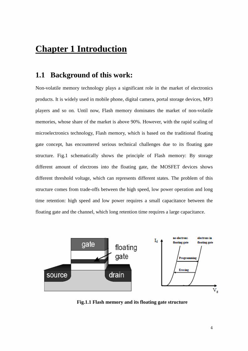
Chapter 1 Introduction
1.1 Background of this work: Non-volatile memory technology plays a significant role in the market of electronics
products. It is widely used in mobile phone, digital camera, portal storage devices, MP3
players and so on. Until now, Flash memory dominates the market of non-volatile
memories, whose share of the market is above 90%. However, with the rapid scaling of
microelectronics technology, Flash memory, which is based on the traditional floating
gate concept, has encountered serious technical challenges due to its floating gate
structure. Fig.1 schematically shows the principle of Flash memory: By storage
different amount of electrons into the floating gate, the MOSFET devices shows
different threshold voltage, which can represents different states. The problem of this
structure comes from trade-offs between the high speed, low power operation and long
time retention: high speed and low power requires a small capacitance between the
floating gate and the channel, which long retention time requires a large capacitance.
Fig.1.1 Flash memory and its floating gate structure
Page 5
5
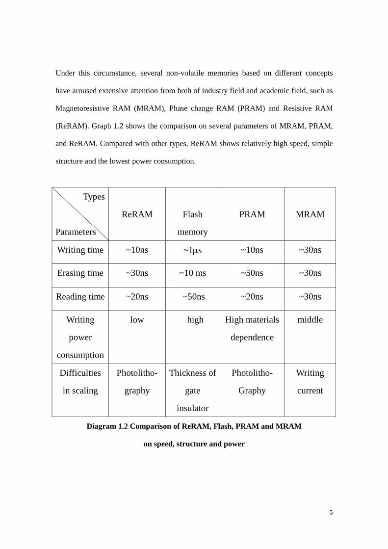
Under this circumstance, several non-volatile memories based on different concepts
have aroused extensive attention from both of industry field and academic field, such as
Magnetoresistive RAM (MRAM), Phase change RAM (PRAM) and Resistive RAM
(ReRAM). Graph 1.2 shows the comparison on several parameters of MRAM, PRAM,
and ReRAM. Compared with other types, ReRAM shows relatively high speed, simple
structure and the lowest power consumption.
Types
Parameters
ReRAM
Flash
memory
PRAM
MRAM
Writing time ~10ns ~1µs ~10ns ~30ns
Erasing time ~30ns ~10 ms ~50ns ~30ns
Reading time ~20ns ~50ns ~20ns ~30ns
Writing
power
consumption
low high High materials
dependence
middle
Difficulties
in scaling
Photolitho-
graphy
Thickness of
gate
insulator
Photolitho-
Graphy
Writing
current
Diagram 1.2 Comparison of ReRAM, Flash, PRAM and MRAM
on speed, structure and power
Page 6
6
1.2 Introduction of ReRAM:
1.2.1 General introduction of ReRAM
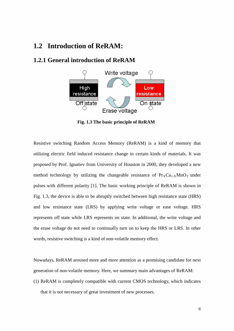
Fig. 1.3 The basic principle of ReRAM
Resistive switching Random Access Memory (ReRAM) is a kind of memory that
utilizing electric field induced resistance change in certain kinds of materials. It was
proposed by Prof. Ignatiev from University of Houston in 2000, they developed a new
method technology by utilizing the changeable resistance of PrXCa1-XMnO3 under
pulses with different polarity [1]. The basic working principle of ReRAM is shown in
Fig. 1.3, the device is able to be abruptly switched between high resistance state (HRS)
and low resistance state (LRS) by applying write voltage or ease voltage. HRS
represents off state while LRS represents on state. In additional, the write voltage and
the erase voltage do not need to continually turn on to keep the HRS or LRS. In other
words, resistive switching is a kind of non-volatile memory effect.
Nowadays, ReRAM aroused more and more attention as a promising candidate for next
generation of non-volatile memory. Here, we summary main advantages of ReRAM:
(1) ReRAM is completely compatible with current CMOS technology, which indicates
that it is not necessary of great investment of new processes.
Page 7
7
(2) ReRAM can be operated under very small power consumption. In the 0.18um
process, the operation current can be controlled at the orders of 10-6A.
(3) ReRAM have simple capacitor structure with two terminals, which is easy to be
integrated to VLSI circuits.
However, ReRAM still facing several challenges to practical application. The key
problem is the stability of the device performance, especially the endurance
characteristics still requires further improvement. Another problem comes from the
switching mechanism, which is still lack of quantified analysis. It is difficult to improve
the device performance without a clear model.
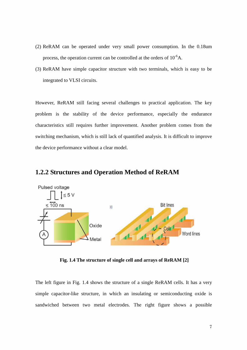
1.2.2 Structures and Operation Method of ReRAM
Fig. 1.4 The structure of single cell and arrays of ReRAM [2]
The left figure in Fig. 1.4 shows the structure of a single ReRAM cells. It has a very
simple capacitor-like structure, in which an insulating or semiconducting oxide is
sandwiched between two metal electrodes. The right figure shows a possible
Page 8
8
“cross-point” array for organizing ReRAM cells. Word and bit lines are used for
selecting a memory cell and writing or reading data, respectively. Cross-point array is a
two dimensional structure, which is relatively simple and requires less fabricating
process. What’s more, cross-point array is able to achieve a very high storage density.
The storage density is determined by the pinch of fabricating process. The definition of
pinch of cross-points array is shown in Fig. 1.5.
Fig. 1.5 The definition of Pinch in cross-points array
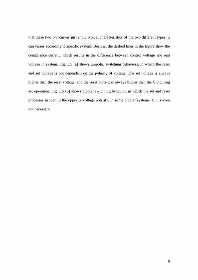
Fig. 1.5 Two types of resistance switching behaviors[3]
The resistance switching behaviors of ReRAM devices can be divided to two basic
types according to their I-V characteristics under sweeping voltage. It should be note
Page 9
9
that these two I-V curves just show typical characteristics of the two different types, it
can varies according to specific system. Besides, the dashed lines in the figure show the
compliance current, which results in the difference between control voltage and real
voltage in system. Fig. 1.5 (a) shows unipolar switching behaviors, in which the reset
and set voltage is not dependent on the polarity of voltage. The set voltage is always
higher than the reset voltage, and the reset current is always higher than the CC during
set operation. Fig. 1.5 (b) shows bipolar switching behavior, in which the set and reset
processes happen in the opposite voltage polarity. In some bipolar systems, CC is even
not necessary.
Page 10
10
1.2.3 Resistive switching mechanism in ReRAM
Although resistance switching behaviors have been found in a wide range of materials,
and lots of models are proposed to explain those phenomenons, there are still lots of
unclear places in the switching mechanisms. Generally, the resistance switching
mechanism can be divided to three types in terms of position. They are interface effect,
bulk effect and combination of bulk effect and interface effect. In this sub-section, we
will introduce some switching mechanism at interface and bulk, respectively.
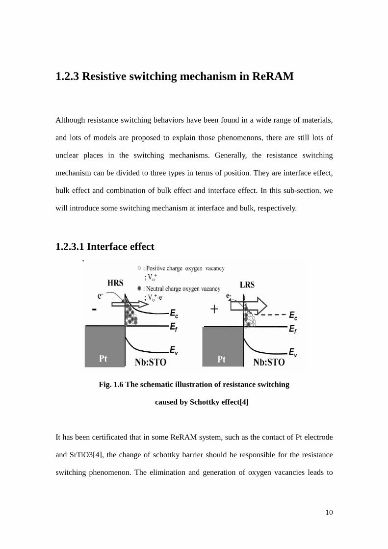
1.2.3.1 Interface effect
Fig. 1.6 The schematic illustration of resistance switching
caused by Schottky effect[4]
It has been certificated that in some ReRAM system, such as the contact of Pt electrode
and SrTiO3[4], the change of schottky barrier should be responsible for the resistance
switching phenomenon. The elimination and generation of oxygen vacancies leads to
Page 11
11
the change of schottky barrier and thus change the tunneling current. For example, in
the case shown in Fig. 1.6, under the effect of negative voltage, the electrons combine
with the oxygen vacancies at the interface. This process results in a wider schottky
barrier and thus a smaller tunneling current, which corresponds to the HRS. On the
contrary, when the positive voltage is applied, opposite process happens and leads to the
LRS.
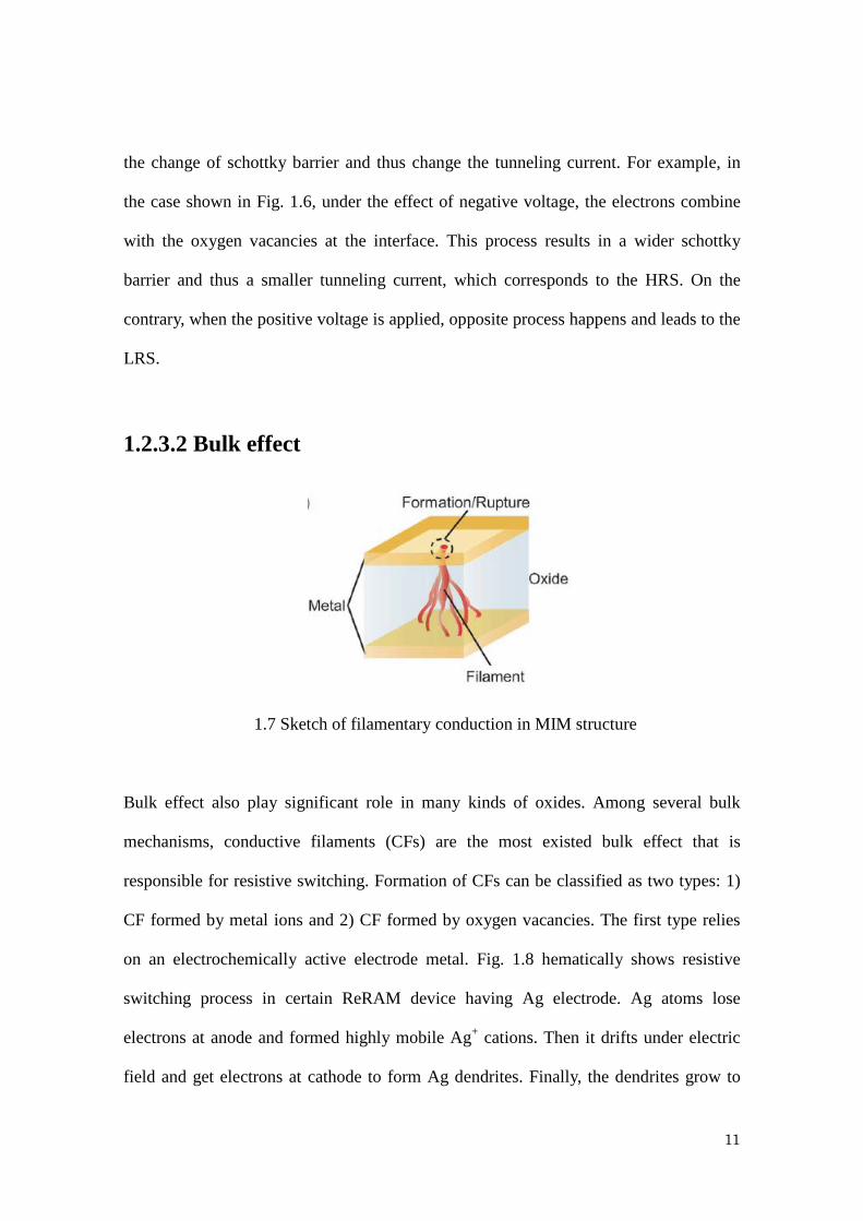
1.2.3.2 Bulk effect
1.7 Sketch of filamentary conduction in MIM structure
Bulk effect also play significant role in many kinds of oxides. Among several bulk
mechanisms, conductive filaments (CFs) are the most existed bulk effect that is
responsible for resistive switching. Formation of CFs can be classified as two types: 1)
CF formed by metal ions and 2) CF formed by oxygen vacancies. The first type relies
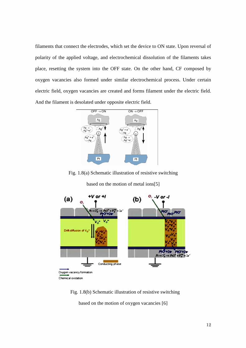
on an electrochemically active electrode metal. Fig. 1.8 hematically shows resistive
switching process in certain ReRAM device having Ag electrode. Ag atoms lose
electrons at anode and formed highly mobile Ag+ cations. Then it drifts under electric
field and get electrons at cathode to form Ag dendrites. Finally, the dendrites grow to
Page 12
12
filaments that connect the electrodes, which set the device to ON state. Upon reversal of
polarity of the applied voltage, and electrochemical dissolution of the filaments takes
place, resetting the system into the OFF state. On the other hand, CF composed by
oxygen vacancies also formed under similar electrochemical process. Under certain
electric field, oxygen vacancies are created and forms filament under the electric field.
And the filament is desolated under opposite electric field.
Fig. 1.8(a) Schematic illustration of resistive switching
based on the motion of metal ions[5]
Fig. 1.8(b) Schematic illustration of resistive switching
based on the motion of oxygen vacancies [6]
Page 13
13
1.4 Parameters for evaluation of memory device
performance:
In order to systematically evaluate the performance of ReRAM devices fabricated in
this studies, we use following indicator to depict and compare performance of devices.
1. Non-volatility: Volatility and Non-volatility are basic character of memory devices,
which indicate that if devices are able to keep the programmed information after take
off electrical powers. For example, SRAM and DRAM is volatile while Flash memory
is non-volatile.
2. Operation voltage: Operation voltage depicts the necessary bias that makes the device
works well. Large operation voltage not only puts negative influences on reliability, but
also increases the complexity of external circuits. Incidentally, large operation voltage is
one of weak points of Flash memory.
3. Memory window: Memory window represents the difference between different
memory states. Its specific definition is different in different types of memory. For
ReRAM, it is defined as the ratio of high resistance states to low resistance states.
Window is directly related to the correction of data reading. A small or unstable window
leads to read errs.
4. Retention: It is defined as the time that devices can keep programmed values. High
quality non-volatile memories are able to keep values more than ten years at room
temperature.
5. Multilevel storage: Multilevel storage indicates the devices have more than two states,
Page 14
14
which improve the storage density. In other words, compared to device with binary
states, a multilevel device can represent more than two values.
6. Endurance: It is the number that how many times the device can be wrote and erased
before failure. For non-volatile memory, 106 times switching is an ideal value.
7. Write/Erase speed (W/E speed): The minimum time required by devices for writing
and erasing. The W/E time of Flash memory is at the order of 10-6 s to 10-3 s. On the
other hand, the W/E time of ReRAM can achieve the orders of 10-100ns.
8. Scaling: The potential of the device for scaling without sacrificing its memory
performance.
Page 15
15
1.5 Purpose of this work Resistive random access memory (ReRAM), which utilizing resistive switching of
certain materials, has attracted much attention as non-volatile memory in the near future
because of its high speed, low consumption and great potential for scalability [3].
Resistive switching behaviors in various insulating oxides, ranging from simple binary
oxides such as NiO2 [6] and TiO2 [7] to complex oxides such as perovskites [8] and
chalcogenides [9], has been reported. Untill now, relatively few studies on the resistive
switching behaviors of cerium oxides has been reported. Among various insulating
oxides, cerium oxides have strong potential for ReRAM application for the following
reasons: 1) cerium oxides have high dielectric constant and moderate band gap, 2)
cerium atom exhibits both +3 and +4 oxidation states in cerium oxides, which is suitable
for valency change switching processes[5], 3) oxygen ions/vacancies, which play a
important role in resistive switching[2], produce high conductivity in CeO2 due to its
fluorite structure, and 4) cerium oxide is easy to react with Si to form silicate [8]. The
last reason provides us a method to modify the structure and concentration of vacancy
in cerium oxide film by forming cerium silicate. In this paper, cerium oxides based
ReRAM devices with silicon buffer layer were fabricated by utilizing W and TiN as
electrodes. The resistive switching behaviors of the devices and the influence of the Si
buffer layer on the resistive switching were investigated in detail.
Page 16
16
Reference:
[1] S.Q. Liu, N.J. Wu, and A. Ignatiev, “ Electric-pulse-induced reversible resistance
change effect in magnetroresisttive films”. Appl. Phys. Lett., 2000(76):2749
[2] R.Waser, et al., “Nanoionics-based resistive switching memories”. Nature materials,
2007(6), 833
[3] A. Sawa, et al., “Resistive switching in transition metal oxides”, materialstoday,
2008(11), 28
[4] A. Sawa, et al., “Hysteretic current-voltage characteristics and resistance switching
at a rectifying Ti/Pr0.7Ca0.3MnO3 interface”. Appl. Phys. Lett., 2004 (85): 4073.
[5] R. Waser, et al., “Electrochemical and Thermochemical Memories”, IEDM, 2009
[6] Seo et al., Appl. Phys. Lett., 85, 23 (2004).
[7] Yang et al., Nature nanotechnology, 3, p.429 (2008)
[8] Szot et al., Nature materials, 5, p. 312 (2006).
[9] Maimon J et al., Chalcogenide-based non-volatile memory technology. IEEE
Aerospace 2001 (2001).
[10] K. Kakushima et al., VLSI Tech. Dig. p.69-70(2010)
Page 17
17
Chapter 2 Fabrication and Characterization Method
In this chapter, all of the fabricating and characterization methods that have been
utilized in studies are introduced. The principles of processes and equipments are
simply discussed and the experiment conditions are also listed.
2.1 Fabrication Method
2.1.1 Si surface cleaning
Si wafer cleaning is critically important in the era of VLSI and ULSI technology. Over
50% of yield losses in integrated circuit fabrication are generally accepted to be due to
microcontamination[1], such as metal contamination, organic contamination, ionic
contamination, and etc. The cleaning process for wafers used in this studies starts from
rinsing Si wafers with running DI (de-ionized) water. The DI water used in this work,
incidentally, has a resistance high than 18.2 MΩcm, while the theoretical resistance of
pure water is 18.25 MΩcm at 25 oC. Then the samples were treated by sulfuric-peroxide
mixture (SPM), which is composed by H2O2 and H2SO4 (H2O2: H2SO4 = 1:4), for
10min at 120oC. During this process, existed organic and metallic contamination was
separated from surfaces of Si wafers because of chemical oxidation of the surfaces.
After that, Si wafers was rinsed with running DI water again. In order to remove the
chemical oxide formed in SPM process, the wafers are further treat by diluted HF
(1%HF) for 1min. Finally, wafers are cleaned again by running DI wafer before next
Page 18
18
fabrication process.
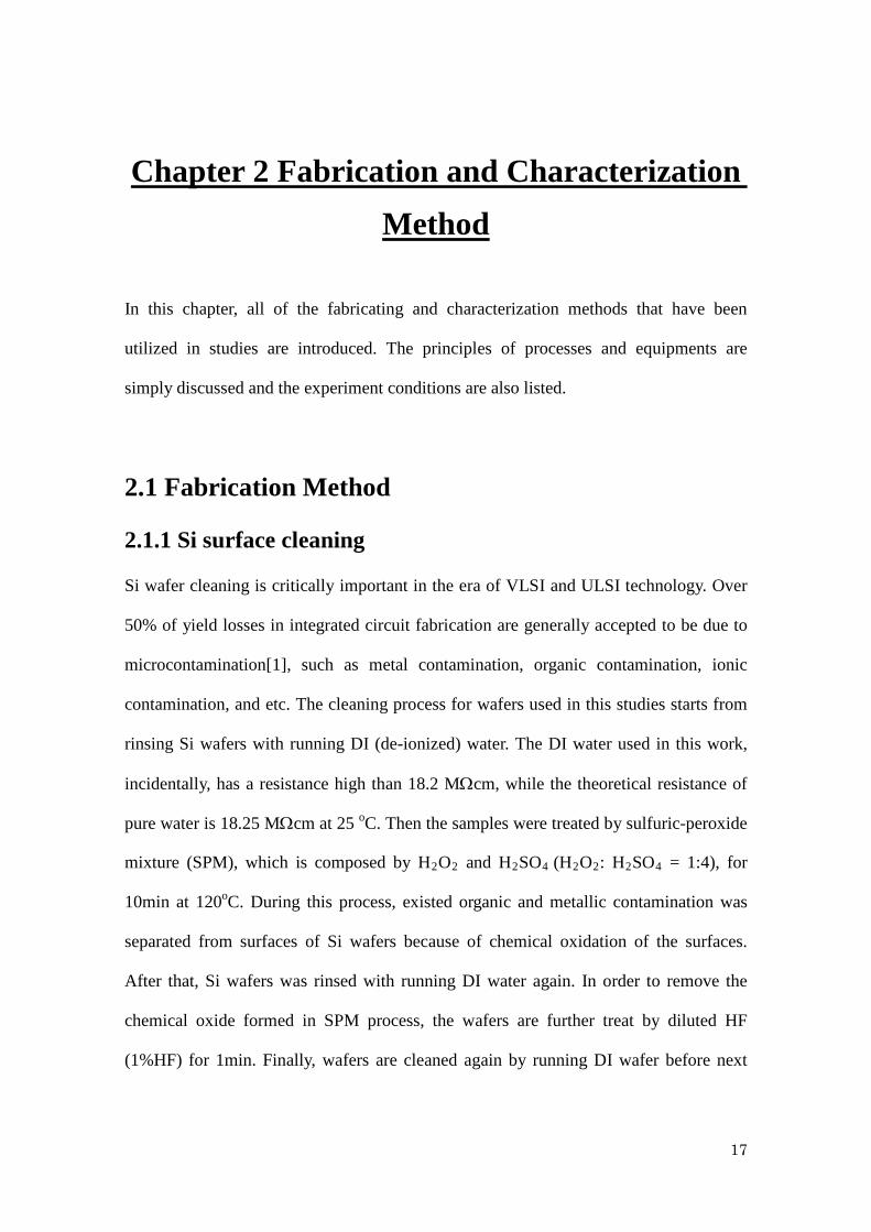
2.1.2 Thermal Oxidation Process
Thermal oxidation is one of key processes in VLSI technology. In the case of silicon
dioxide, it can be classified to two types: wet oxidation ( Si + 2H2O = SiO2 + 2H2,
800oC-1100oC) and dry oxidation ( Si + O2 = 2SiO2, 800oC-1100oC). Wet oxidation is
suitable for growth of thick silicon dioxide because of its relatively high growth rate,
while dry oxidation is rather slow but easily controllable. In this work, a layer of SiO2
(about 200nm) is grown on a Si wafer by dry oxidation in an oxidation furnace, whose
structure is shown in Fig.X. One of critical challenges in thermal oxidation is creation a
gas ambient with precise, constant and uniform temperature. By utilizing three heaters
in different part of the quartz tube, the temperature becomes more uniform in the whole
tube. In addition, only a small localized region in the middle of tube is used for thermal
oxidation, which further improves the uniformity of the temperature and the mass flow.
The samples are set on a small quartz boat and slowly send into the middle of the tube
by a quartz rod. The mass flow of O2 is controlled to be 1L/min and the oxidation is
continued for 2 hours at 1000oC.
Page 19
19
Fig. 2.1 (a) Schematic illustration of the oxidation furnace
Fig.2.1 (b) Photo of oxidation furnace
Page 20
20
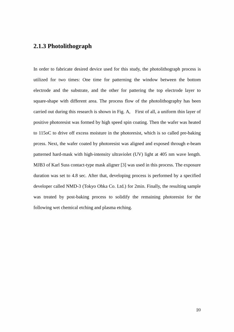
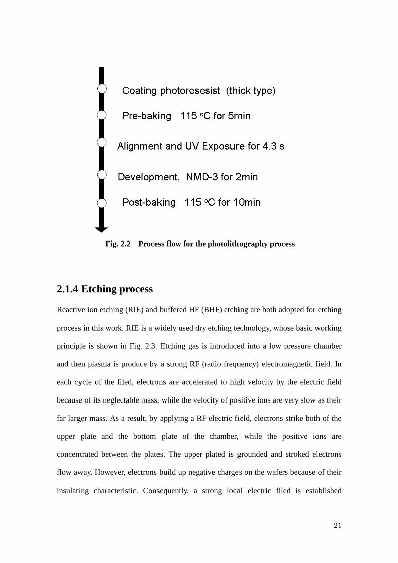
2.1.3 Photolithograph
In order to fabricate desired device used for this study, the photolithograph process is
utilized for two times: One time for patterning the window between the bottom
electrode and the substrate, and the other for pattering the top electrode layer to
square-shape with different area. The process flow of the photolithography has been
carried out during this research is shown in Fig. A, First of all, a uniform thin layer of
positive photoresist was formed by high speed spin coating. Then the wafer was heated
to 115oC to drive off excess moisture in the photoresist, which is so called pre-baking
prcess. Next, the wafer coated by photoresist was aligned and exposed through e-beam
patterned hard-mask with high-intensity ultraviolet (UV) light at 405 nm wave length.
MJB3 of Karl Suss contact-type mask aligner [3] was used in this process. The exposure
duration was set to 4.8 sec. After that, developing process is performed by a specified
developer called NMD-3 (Tokyo Ohka Co. Ltd.) for 2min. Finally, the resulting sample
was treated by post-baking process to solidify the remaining photoresist for the
following wet chemical etching and plasma etching.
Page 21
21
Fig. 2.2 Process flow for the photolithography process
2.1.4 Etching process
Reactive ion etching (RIE) and buffered HF (BHF) etching are both adopted for etching
process in this work. RIE is a widely used dry etching technology, whose basic working
principle is shown in Fig. 2.3. Etching gas is introduced into a low pressure chamber
and then plasma is produce by a strong RF (radio frequency) electromagnetic field. In
each cycle of the filed, electrons are accelerated to high velocity by the electric field
because of its neglectable mass, while the velocity of positive ions are very slow as their
far larger mass. As a result, by applying a RF electric field, electrons strike both of the
upper plate and the bottom plate of the chamber, while the positive ions are
concentrated between the plates. The upper plated is grounded and stroked electrons
flow away. However, electrons build up negative charges on the wafers because of their
insulating characteristic. Consequently, a strong local electric filed is established
Page 22
22
between the positive etching ions and the negative wafers. The ions bombard the sample
and chemically react with certain kind of material, which results in etching selected part
of the sample. Furthermore, physical sputtering of the sample surface also happens
during this process. Because of the vertical electric field, RIE shows anisotropic etching
profile. In this work, SF6 was used to etching the W electrode layer and O2 was used to
remove the photoresist from the etched wafer. On the other hand, BHF is also adopted
for wet etching of silicon dioxide over silicon wafers, which is an isotropic etching
process. BHF is composed by HF, NH4F and H2O, and it can etching silicon dioxide in
a controlled speed (100nm/min for BHF used in this work),
Fig. 2.3 Schematic illustration of Reactive ion etching
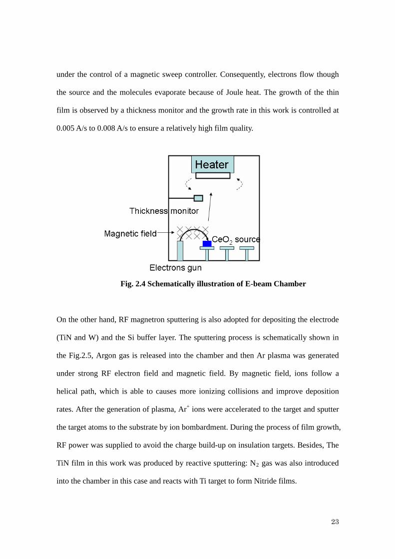
2.1.4 E-beam evaporation and RF magnetron sputtering:
E-beam evaporation and RF magnetron sputtering are used extensively in the
semiconductor industry to deposit thin films of a large amount of materials in VLSI
technology. E-beam evaporation is employed for depositing CeO2 thin film in this work.
Deposition is carried out at chamber in ultra high vacuum state (10-8~10-9 Torr). The
sample is heated to 300 oC and rotated at a constant speed in advance. Electron beam,
which is accelerated by a 5 KV electric field, is generated and bombard to the source
Page 23
23
under the control of a magnetic sweep controller. Consequently, electrons flow though
the source and the molecules evaporate because of Joule heat. The growth of the thin
film is observed by a thickness monitor and the growth rate in this work is controlled at
0.005 A/s to 0.008 A/s to ensure a relatively high film quality.
Fig. 2.4 Schematically illustration of E-beam Chamber
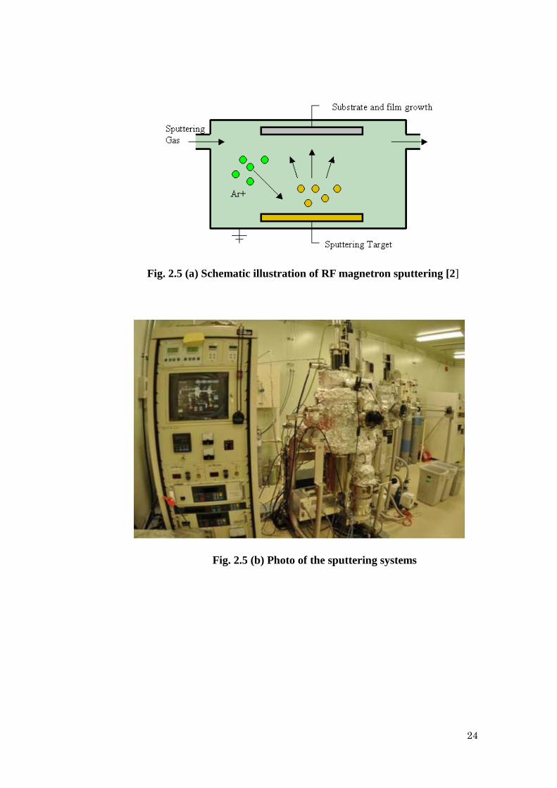
On the other hand, RF magnetron sputtering is also adopted for depositing the electrode
(TiN and W) and the Si buffer layer. The sputtering process is schematically shown in
the Fig.2.5, Argon gas is released into the chamber and then Ar plasma was generated
under strong RF electron field and magnetic field. By magnetic field, ions follow a
helical path, which is able to causes more ionizing collisions and improve deposition
rates. After the generation of plasma, Ar+ ions were accelerated to the target and sputter
the target atoms to the substrate by ion bombardment. During the process of film growth,
RF power was supplied to avoid the charge build-up on insulation targets. Besides, The
TiN film in this work was produced by reactive sputtering: N2 gas was also introduced
into the chamber in this case and reacts with Ti target to form Nitride films.
Page 24
24
Fig. 2.5 (a) Schematic illustration of RF magnetron sputtering [2]
Fig. 2.5 (b) Photo of the sputtering systems
Page 25
25
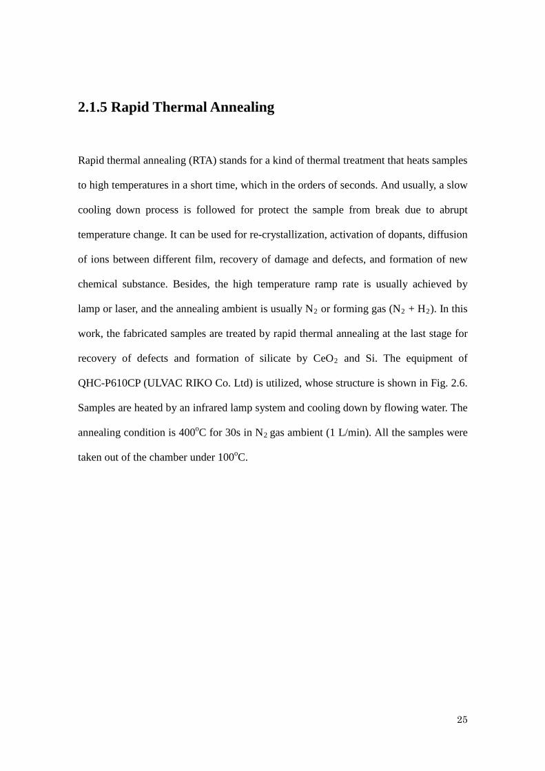
2.1.5 Rapid Thermal Annealing
Rapid thermal annealing (RTA) stands for a kind of thermal treatment that heats samples
to high temperatures in a short time, which in the orders of seconds. And usually, a slow
cooling down process is followed for protect the sample from break due to abrupt
temperature change. It can be used for re-crystallization, activation of dopants, diffusion
of ions between different film, recovery of damage and defects, and formation of new
chemical substance. Besides, the high temperature ramp rate is usually achieved by
lamp or laser, and the annealing ambient is usually N2 or forming gas (N2 + H2). In this
work, the fabricated samples are treated by rapid thermal annealing at the last stage for
recovery of defects and formation of silicate by CeO2 and Si. The equipment of
QHC-P610CP (ULVAC RIKO Co. Ltd) is utilized, whose structure is shown in Fig. 2.6.
Samples are heated by an infrared lamp system and cooling down by flowing water. The
annealing condition is 400oC for 30s in N2 gas ambient (1 L/min). All the samples were
taken out of the chamber under 100oC.
Page 26
26
Fig. 2.6 (a) Schematic illustration of the infrared annealing furnace
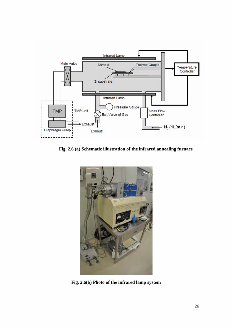
Fig. 2.6(b) Photo of the infrared lamp system
Page 27
27
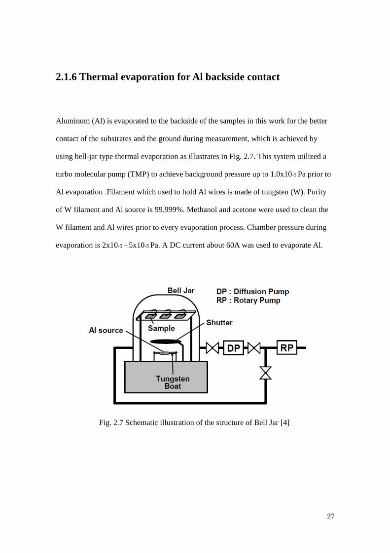
2.1.6 Thermal evaporation for Al backside contact
Aluminum (Al) is evaporated to the backside of the samples in this work for the better
contact of the substrates and the ground during measurement, which is achieved by
using bell-jar type thermal evaporation as illustrates in Fig. 2.7. This system utilized a
turbo molecular pump (TMP) to achieve background pressure up to 1.0x10⁻⁵ Pa prior to
Al evaporation .Filament which used to hold Al wires is made of tungsten (W). Purity
of W filament and Al source is 99.999%. Methanol and acetone were used to clean the
W filament and Al wires prior to every evaporation process. Chamber pressure during
evaporation is 2x10⁻⁵ - 5x10⁻⁵ Pa. A DC current about 60A was used to evaporate Al.
Fig. 2.7 Schematic illustration of the structure of Bell Jar [4]
Page 28
28
2.2 Characterization method
2.2.1 Current-voltage measurement
I-V measurements were done on HP4156A semiconductor parameter analyzer. In order
to tracing the resistance switching behaviors, a sweep voltage ranging for -10V to 10V,
whose step is 0.05 V, is used. Besides, different compliance current ranging from 1mA
to 5mA is also set to protect the device from break down. In addition, in order to
investigate the conduction mechanism of different conduction state, I-V measurement in
different temperature is also carried out.
Reference [1] Wemer Kern, The Evolution of Silicon Wafer Cleaning Technology, J. Electronchem.
Soc., Vol. 137, No.6, June 1990
[2] http://en.wikipedia.org/wiki/Sputter_deposition
[3] http://www.suss.com
[4] Jaeyeol Song, doctor thesis (2010), Tokyo Institute of Technology
Page 29
29
Chapter 3:
Resistive switching behaivors in the RRAM device
having W/CeO2/Si/TiN Structure
3.1 Device design and fabrication
Page 30
30
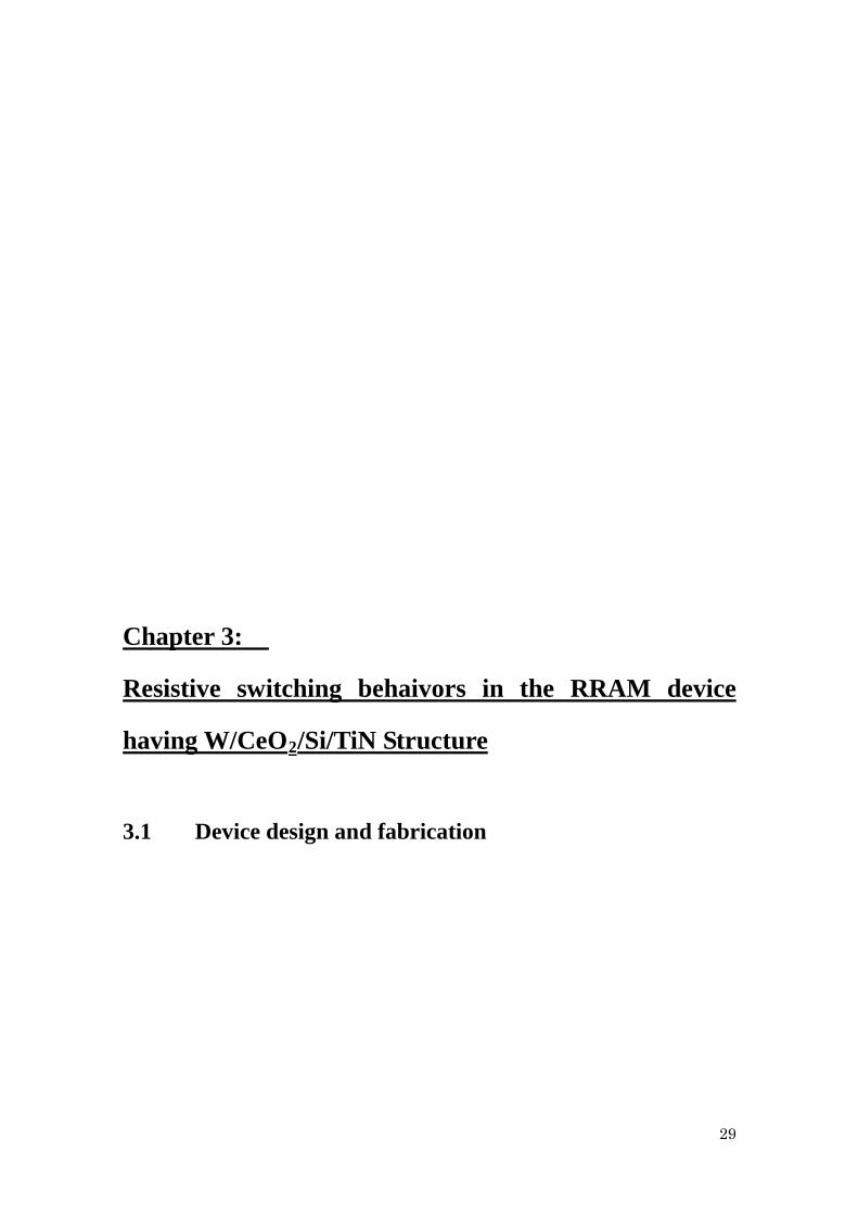
Fig. 3.1.1 Schematic illustration of the ReRAM device having W/CeO2/Si/TiN
structure and the measurement circuit
The structure of the device and the measurement circuit are schematically shown in Fig.
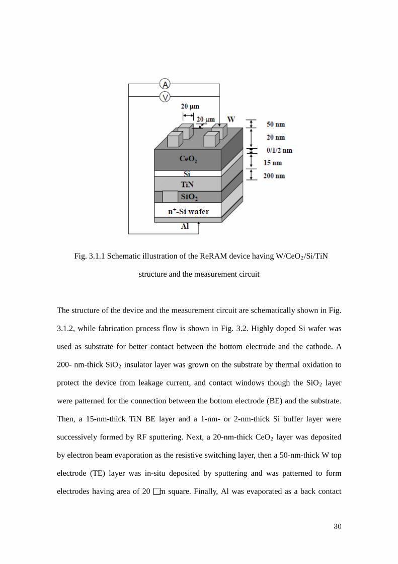
3.1.2, while fabrication process flow is shown in Fig. 3.2. Highly doped Si wafer was
used as substrate for better contact between the bottom electrode and the cathode. A
200- nm-thick SiO2 insulator layer was grown on the substrate by thermal oxidation to
protect the device from leakage current, and contact windows though the SiO2 layer
were patterned for the connection between the bottom electrode (BE) and the substrate.
Then, a 15-nm-thick TiN BE layer and a 1-nm- or 2-nm-thick Si buffer layer were
successively formed by RF sputtering. Next, a 20-nm-thick CeO2 layer was deposited
by electron beam evaporation as the resistive switching layer, then a 50-nm-thick W top
electrode (TE) layer was in-situ deposited by sputtering and was patterned to form
electrodes having area of 20 m square. Finally, Al was evaporated as a back contact
Page 31
31
followed by rapid thermal annealing (RTA) in N2 ambient for 30 s at 400oC.
Furthermore, the device without Si buffer layer was also fabricated to evaluate the
influence of Si buffer layer on switching characteristics.
Fig. 3.1.2 W/CeO2/Si/TiN device fabrication process flow
3.2 Resistive switching behaviors
Page 32
32
1.0E-10
1.0E-09
1.0E-08
1.0E-07
1.0E-06
1.0E-05
1.0E-04
1.0E-03
1.0E-02
-3 -2 -1 0 1 2 3 4
1st cycle
2nd cycle
10th cycle
Bias ( V )
Cur
rent
(A)
Formingprocess
④①
②③
With 1nm Si
HRS
LRS
SETRESET
C.C.= 1mA
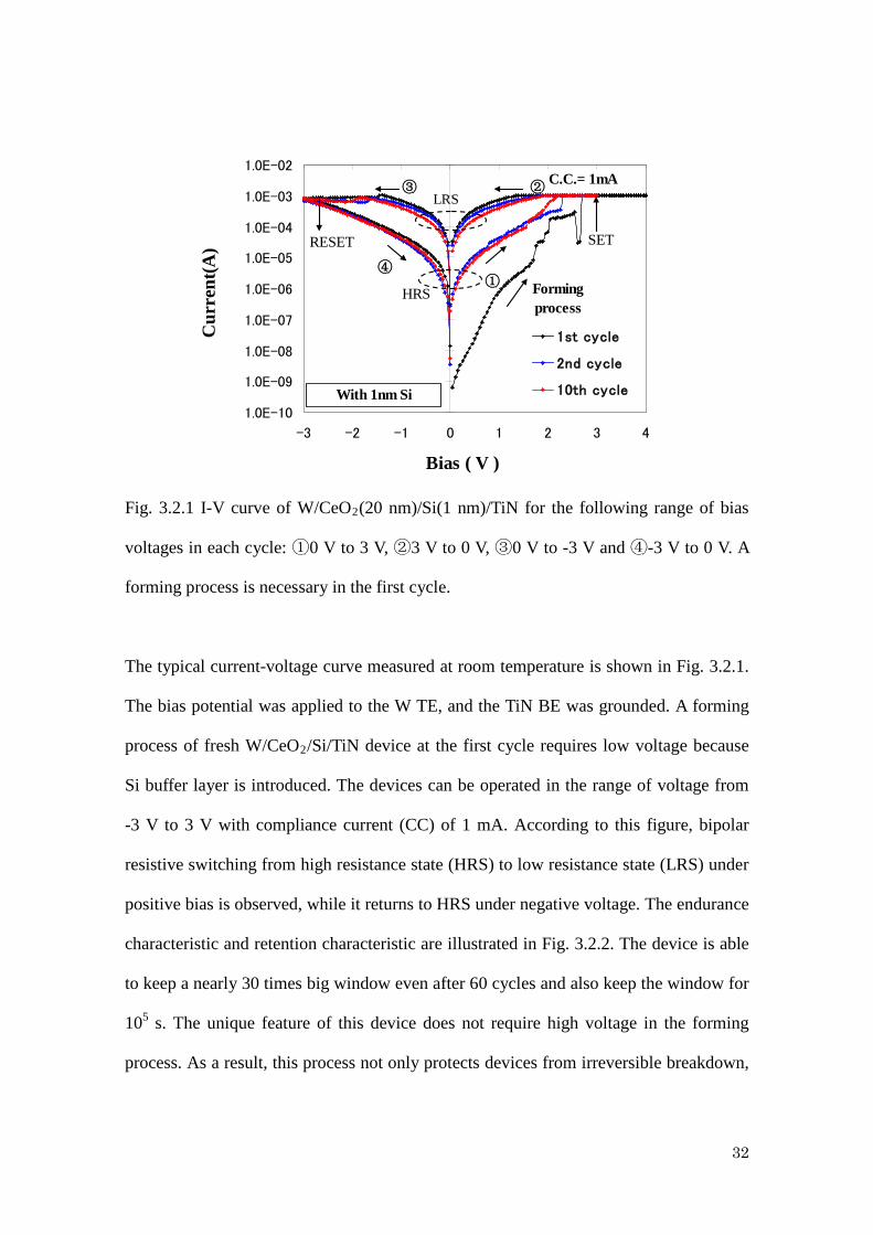
Fig. 3.2.1 I-V curve of W/CeO2(20 nm)/Si(1 nm)/TiN for the following range of bias
voltages in each cycle: ①0 V to 3 V, ②3 V to 0 V, ③0 V to -3 V and ④-3 V to 0 V. A
forming process is necessary in the first cycle.
The typical current-voltage curve measured at room temperature is shown in Fig. 3.2.1.
The bias potential was applied to the W TE, and the TiN BE was grounded. A forming
process of fresh W/CeO2/Si/TiN device at the first cycle requires low voltage because
Si buffer layer is introduced. The devices can be operated in the range of voltage from
-3 V to 3 V with compliance current (CC) of 1 mA. According to this figure, bipolar
resistive switching from high resistance state (HRS) to low resistance state (LRS) under
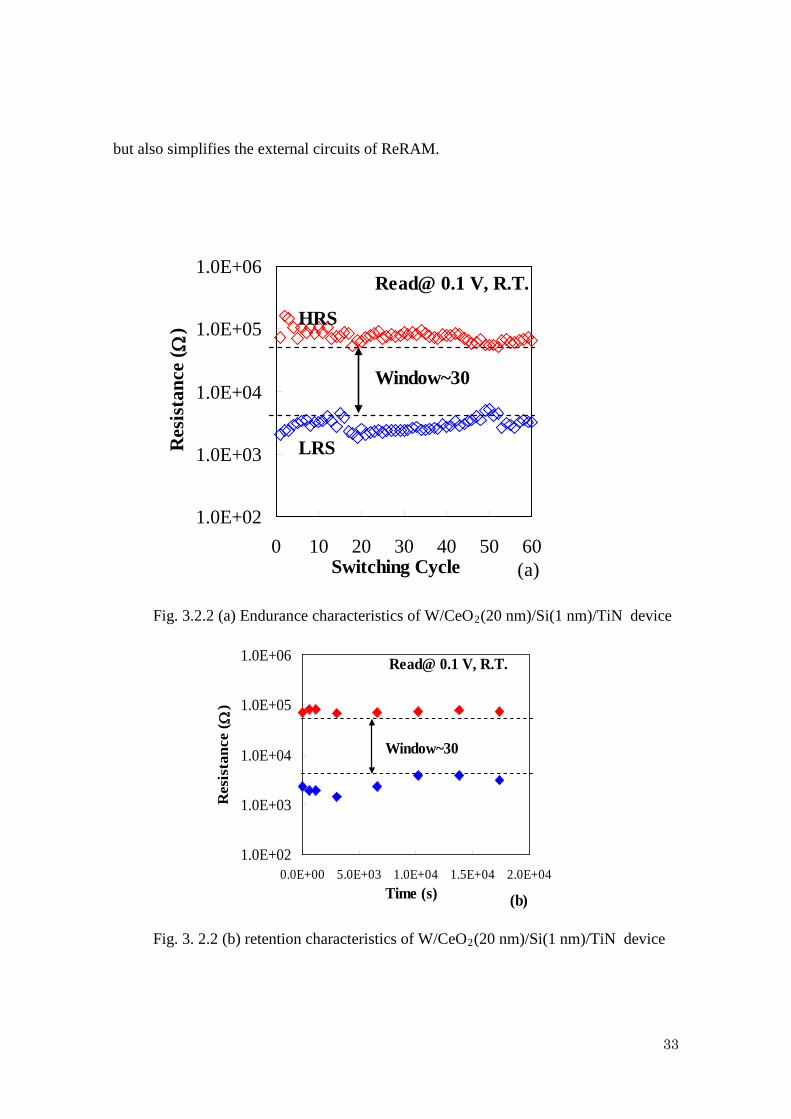
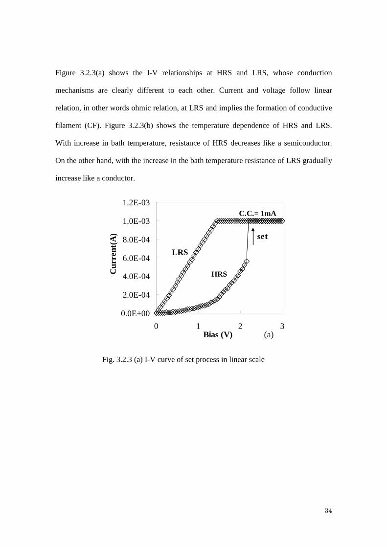
positive bias is observed, while it returns to HRS under negative voltage. The endurance
characteristic and retention characteristic are illustrated in Fig. 3.2.2. The device is able
to keep a nearly 30 times big window even after 60 cycles and also keep the window for
105 s. The unique feature of this device does not require high voltage in the forming
process. As a result, this process not only protects devices from irreversible breakdown,
Page 33
33
but also simplifies the external circuits of ReRAM.
1.0E+02
1.0E+03
1.0E+04
1.0E+05
1.0E+06
0 10 20 30 40 50 60Switching Cycle
Res
ista
nce
( Ω)
Window~30
HRS
LRS
Read@ 0.1 V, R.T.
(a)
Fig. 3.2.2 (a) Endurance characteristics of W/CeO2(20 nm)/Si(1 nm)/TiN device
1.0E+02
1.0E+03
1.0E+04
1.0E+05
1.0E+06
0.0E+00 5.0E+03 1.0E+04 1.5E+04 2.0E+04Time (s)
Res
ista
nce
( Ω)
Read@ 0.1 V, R.T.
Window~30
(b)
Fig. 3. 2.2 (b) retention characteristics of W/CeO2(20 nm)/Si(1 nm)/TiN device
Page 34
34
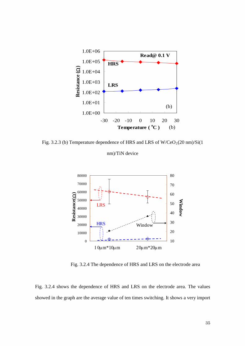
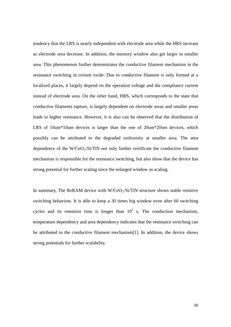
Figure 3.2.3(a) shows the I-V relationships at HRS and LRS, whose conduction
mechanisms are clearly different to each other. Current and voltage follow linear
relation, in other words ohmic relation, at LRS and implies the formation of conductive
filament (CF). Figure 3.2.3(b) shows the temperature dependence of HRS and LRS.
With increase in bath temperature, resistance of HRS decreases like a semiconductor.
On the other hand, with the increase in the bath temperature resistance of LRS gradually
increase like a conductor.
0.0E+00
2.0E-04
4.0E-04
6.0E-04
8.0E-04
1.0E-03
1.2E-03
0 1 2 3Bias (V)
Cur
rent
(A) set
LRS
HRS
C.C.= 1mA
(a)
Fig. 3.2.3 (a) I-V curve of set process in linear scale
Page 35
35
1.0E+00
1.0E+01
1.0E+02
1.0E+03
1.0E+04
1.0E+05
1.0E+06
-30 -20 -10 0 10 20 30
(b)
Temperature ( oC )
Resis
tanc
e (Ω
)
Read@ 0.1 V
(b)
HRS
LRS
Fig. 3.2.3 (b) Temperature dependence of HRS and LRS of W/CeO2(20 nm)/Si(1
nm)/TiN device
0
10000
20000
30000
40000
50000
60000
70000
80000
0.5 1 1.5 2 2.5
10
20
30
40
50
60
70
80
Res
istan
ce( Ω
)
HRS
LRS
Window
Window
10µm*10µm 20µm*20µm
Fig. 3.2.4 The dependence of HRS and LRS on the electrode area
Fig. 3.2.4 shows the dependence of HRS and LRS on the electrode area. The values
showed in the graph are the average value of ten times switching. It shows a very import
Page 36
36
tendency that the LRS is nearly independent with electrode area while the HRS increase
as electrode area decrease. In addition, the memory window also get larger in smaller
area. This phenomenon further demonstrates the conductive filament mechanism in the
resistance switching in cerium oxide: Due to conductive filament is only formed at a
localized places, it largely depend on the operation voltage and the compliance current
instead of electrode area. On the other hand, HRS, which corresponds to the state that
conductive filaments rapture, is largely dependent on electrode areas and smaller areas
leads to higher resistance. However, it is also can be observed that the distribution of
LRS of 10um*10um devices is larger than the one of 20um*20um devices, which
possibly can be attributed to the degraded uniformity at smaller area. The area
dependence of the W/CeO2/Si/TiN not only further certificate the conductive filament
mechanism is responsible for the resistance switching, but also show that the device has
strong potential for further scaling since the enlarged window as scaling.
In summary, The ReRAM device with W/CeO2/Si/TiN structure shows stable resistive
switching behaviors. It is able to keep a 30 times big window even after 60 switching
cycles and its retention time is longer than 105 s. The conduction mechanism,
temperature dependency and area dependency indicates that the resistance switching can
be attributed to the conductive filament mechanism[1]. In addition, the device shows
strong potentials for further scalability.
Page 37
37
3.3 The effect of Si buffer layer
1.0E-101.0E-091.0E-081.0E-071.0E-061.0E-051.0E-041.0E-031.0E-021.0E-01
-3 -2 -1 0 1 2 3 4 5 6 7 8
1st cycle
2nd cycle
Typical switchingof device with Si
Bias ( V )
Cur
rent
(A)
①
②③
④
(a)
C.C.= 5mA
C.C.= 1mA
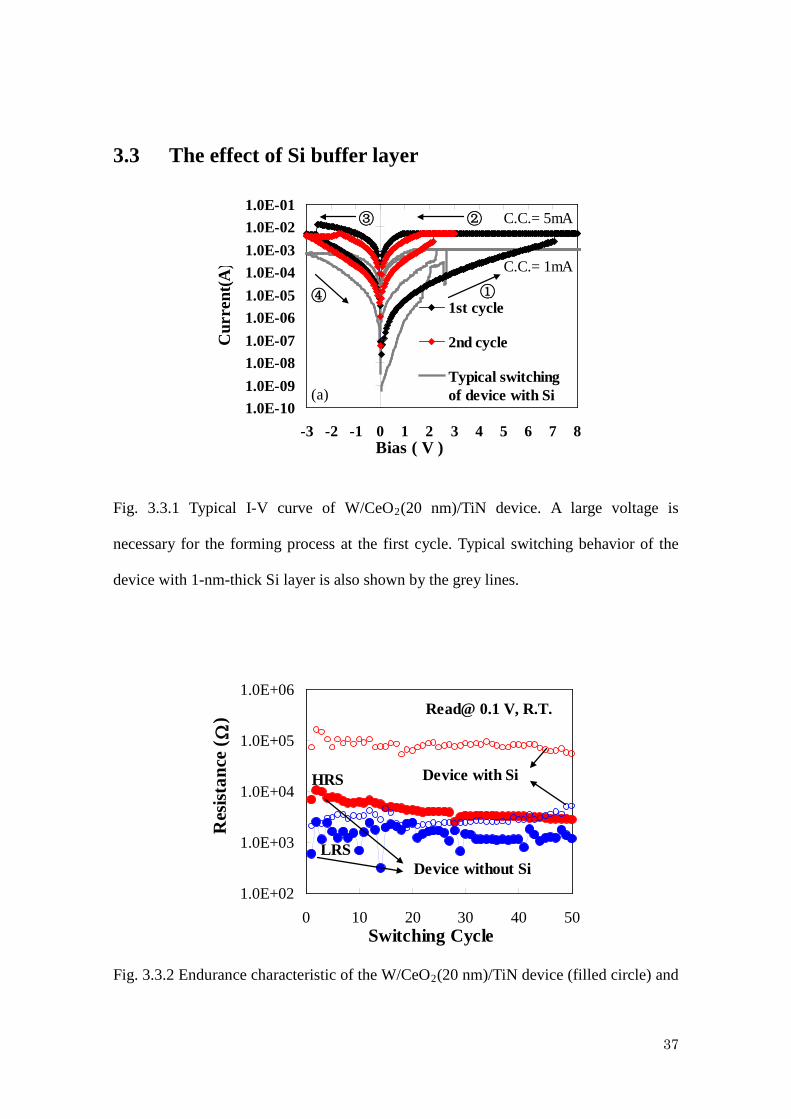
Fig. 3.3.1 Typical I-V curve of W/CeO2(20 nm)/TiN device. A large voltage is
necessary for the forming process at the first cycle. Typical switching behavior of the
device with 1-nm-thick Si layer is also shown by the grey lines.
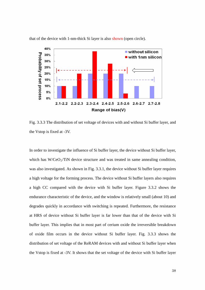
1.0E+02
1.0E+03
1.0E+04
1.0E+05
1.0E+06
0 10 20 30 40 50Switching Cycle
Res
istan
ce (Ω
)
HRS
LRS
Read@ 0.1 V, R.T.
Device without Si
Device with Si
Fig. 3.3.2 Endurance characteristic of the W/CeO2(20 nm)/TiN device (filled circle) and
Page 38
38
that of the device with 1-nm-thick Si layer is also shown (open circle).
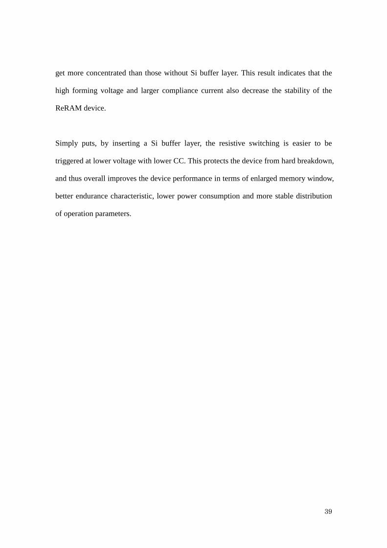
Fig. 3.3.3 The distribution of set voltage of devices with and without Si buffer layer, and
the Vstop is fixed at -3V.
In order to investigate the influence of Si buffer layer, the device without Si buffer layer,
which has W/CeO2/TiN device structure and was treated in same annealing condition,
was also investigated. As shown in Fig. 3.3.1, the device without Si buffer layer requires
a high voltage for the forming process. The device without Si buffer layers also requires
a high CC compared with the device with Si buffer layer. Figure 3.3.2 shows the
endurance characteristic of the device, and the window is relatively small (about 10) and
degrades quickly in accordance with switching is repeated. Furthermore, the resistance
at HRS of device without Si buffer layer is far lower than that of the device with Si
buffer layer. This implies that in most part of cerium oxide the irreversible breakdown
of oxide film occurs in the device without Si buffer layer. Fig. 3.3.3 shows the
distribution of set voltage of the ReRAM devices with and without Si buffer layer when
the Vstop is fixed at -3V. It shows that the set voltage of the device with Si buffer layer
Page 39
39
get more concentrated than those without Si buffer layer. This result indicates that the
high forming voltage and larger compliance current also decrease the stability of the
ReRAM device.
Simply puts, by inserting a Si buffer layer, the resistive switching is easier to be
triggered at lower voltage with lower CC. This protects the device from hard breakdown,
and thus overall improves the device performance in terms of enlarged memory window,
better endurance characteristic, lower power consumption and more stable distribution
of operation parameters.
Page 40
40
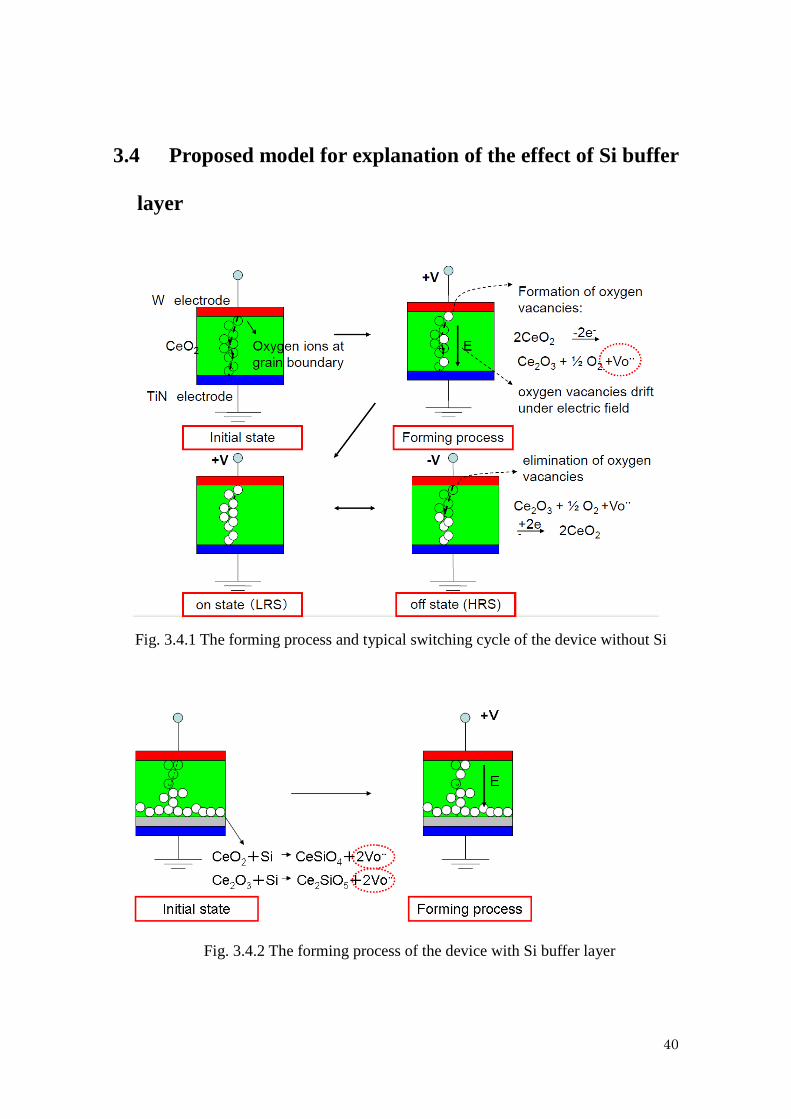
3.4 Proposed model for explanation of the effect of Si buffer
layer
Fig. 3.4.1 The forming process and typical switching cycle of the device without Si
Fig. 3.4.2 The forming process of the device with Si buffer layer
Page 41
41
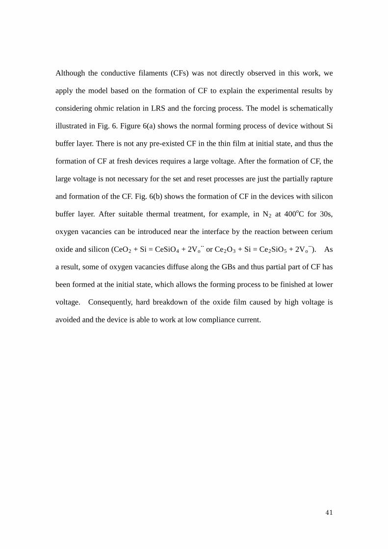
Although the conductive filaments (CFs) was not directly observed in this work, we
apply the model based on the formation of CF to explain the experimental results by
considering ohmic relation in LRS and the forcing process. The model is schematically
illustrated in Fig. 6. Figure 6(a) shows the normal forming process of device without Si
buffer layer. There is not any pre-existed CF in the thin film at initial state, and thus the
formation of CF at fresh devices requires a large voltage. After the formation of CF, the
large voltage is not necessary for the set and reset processes are just the partially rapture
and formation of the CF. Fig. 6(b) shows the formation of CF in the devices with silicon
buffer layer. After suitable thermal treatment, for example, in N2 at 400oC for 30s,
oxygen vacancies can be introduced near the interface by the reaction between cerium
oxide and silicon (CeO2 + Si = CeSiO4 + 2Vo·· or Ce2O3 + Si = Ce2SiO5 + 2Vo
··). As
a result, some of oxygen vacancies diffuse along the GBs and thus partial part of CF has
been formed at the initial state, which allows the forming process to be finished at lower
voltage. Consequently, hard breakdown of the oxide film caused by high voltage is
avoided and the device is able to work at low compliance current.
Page 42
42
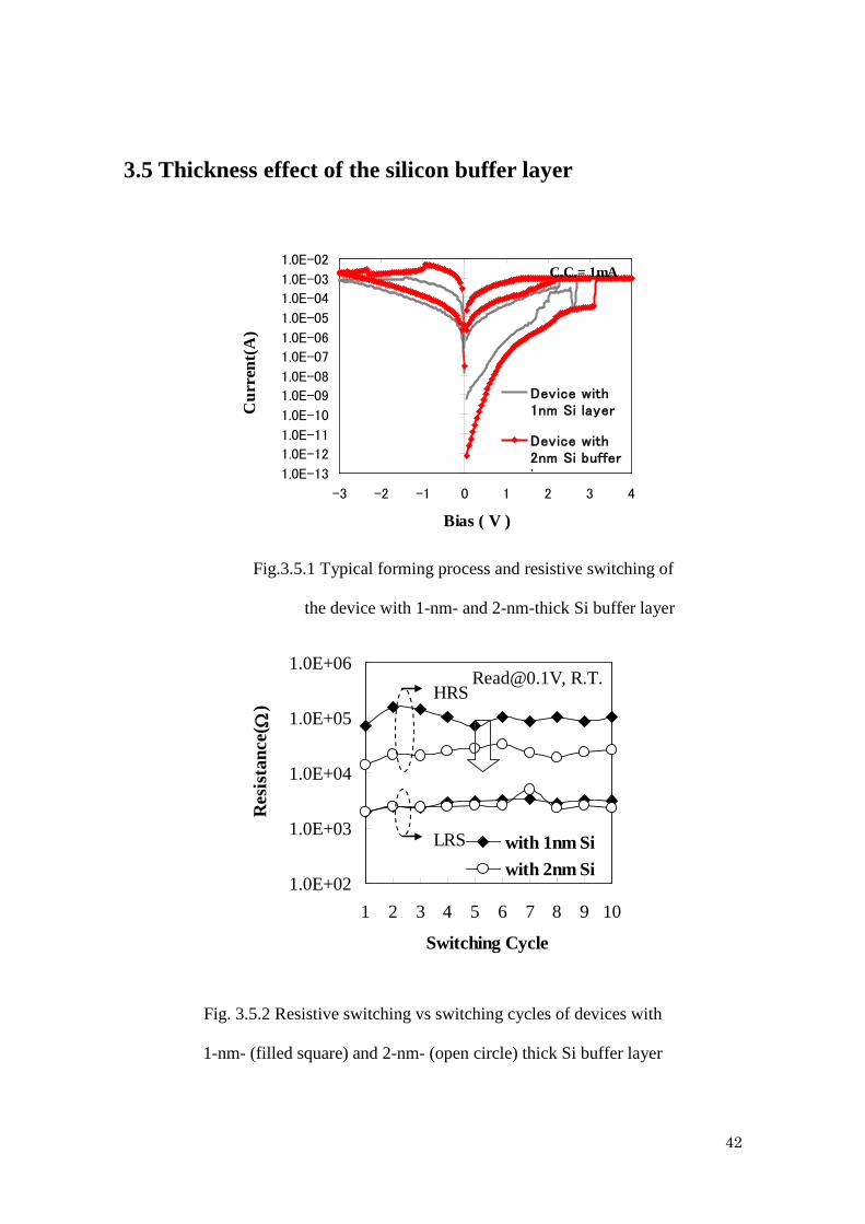
3.5 Thickness effect of the silicon buffer layer
1.0E-13
1.0E-12
1.0E-11
1.0E-10
1.0E-09
1.0E-08
1.0E-07
1.0E-06
1.0E-05
1.0E-04
1.0E-03
1.0E-02
-3 -2 -1 0 1 2 3 4
Device with1nm Si layer
Device with2nm Si bufferlayer
Bias ( V )
Cur
rent
(A)
C.C.= 1mA
Fig.3.5.1 Typical forming process and resistive switching of
the device with 1-nm- and 2-nm-thick Si buffer layer
1.0E+02
1.0E+03
1.0E+04
1.0E+05
1.0E+06
1 2 3 4 5 6 7 8 9 10
with 1nm Siwith 2nm Si
Switching Cycle
Res
ista
nce(Ω
)
[email protected] , R.T.
LRS
Fig. 3.5.2 Resistive switching vs switching cycles of devices with
1-nm- (filled square) and 2-nm- (open circle) thick Si buffer layer
Page 43
43
The influence of Si buffer-layer-thickness on the resistive switching of W/CeO2 (20
nm)/Si(2nm)/TiN device, which was treated by same annealing condition, was also
studied, whose typical I-V curve and C-V characteristics and the change in resistance as
a function of switching cycles are shown in Figs. 3.5.1 and 3.5.2, respectively, where
the corresponding values of the device with 1-nm-thick Si buffer layer are also shown
for comparison. As shown in Fig. 8, the window of the device with 2-nm-thick Si buffer
layer is smaller than those with 1-nm-thick Si buffer layer. Furthermore, two kinds of
devices have similar LRS and the difference comes from HRS. Using the
aforementioned model, the thickness effect of the Si buffer layer can be explained by
the following mechanism Although thicker Si layer results in the introduction of lager
amount of oxygen vacancies, the formation of CFs is largely determined by set voltage
and CC. Because the devices with 1-nm- and 2-nm-thick Si buffer layer are operated at
close voltage with the same CC, similar CFs are formed to have similar LRS in these
devices. However, lager amount of oxygen vacancies make the rapture of CFs become
more difficult. As a result, the device with 2nm Si layer is not able to reset to a HRS as
high as the one of the device with 1nm, which also can be observed in Fig.3.5.1. The
influence of the Si buffer-layer-thickness on the resistive switching indicates that in
order to achieve the best performance of the devices, the thickness of Si buffer layer
should be optimized.
Page 44
44
3.6 Conclusion
In summary, W/CeO2/Si/TiN ReRAM device shows bipolar resistance switching
behaviors. It is able to keep a nearly 30 times big window even after 60 cycles and also
keep the window for 105 s. The conduction mechanism of LRS, the temperature
dependency of HRS and LRS, and also the area dependency demonstrates that the
conductive filament mechanism should be responsible for the resistance switching. It
was also find that the Si buffer layer play a significant role in such resistance switching
behaviors, which effectively increase the memory performance of the devices. The Si
buffer layer not only decreases the voltage for the forming process, but also enlarges the
window, improves the endurance characteristic and lowers power consumption.
Furthermore, a model based on conductive filament mechanism was found to explain
the physical effect of the silicon buffer layer, which is attributed to the introduction of
additional oxygen vacancies and thus help resistance switches more easily. Finally, the
thickness effect of the Si buffer layer is investigated. It is conclude that thicker Si buffer
layer leads to larger amount of oxygen vacancies and the thickness of Si buffer layer
should be should be optimized to obtain the best performance of the device.
Reference
[1] D.Lee et al. IEDM, 2006, p.796
Page 45
45
Champter 4: Modeling of the resistance switching
behaviors in W/CeO2/Si/TiN device
4.1 The influence of Vstop on the resistance switching
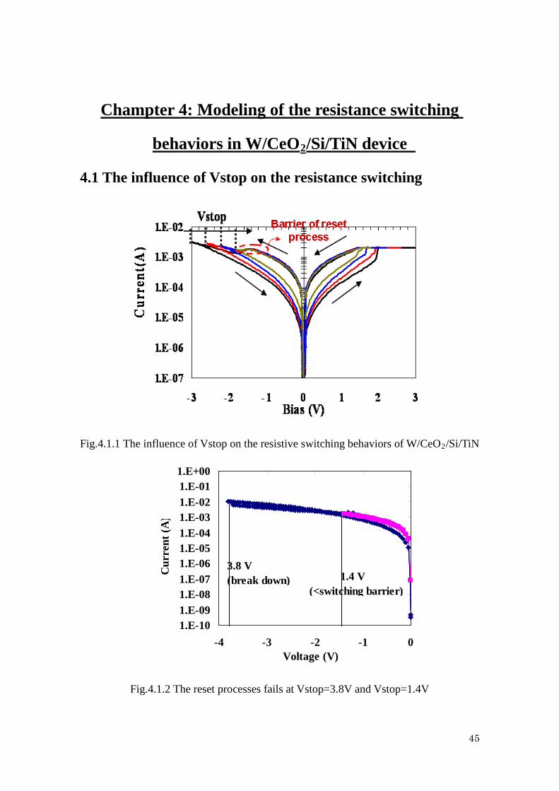
Fig.4.1.1 The influence of Vstop on the resistive switching behaviors of W/CeO2/Si/TiN
1.E-101.E-091.E-081.E-071.E-061.E-051.E-041.E-031.E-021.E-011.E+00
-4 -3 -2 -1 0Voltage (V)
Cur
rent
(A)
3.8 V(break down) 1.4 V
(<switching barrier)
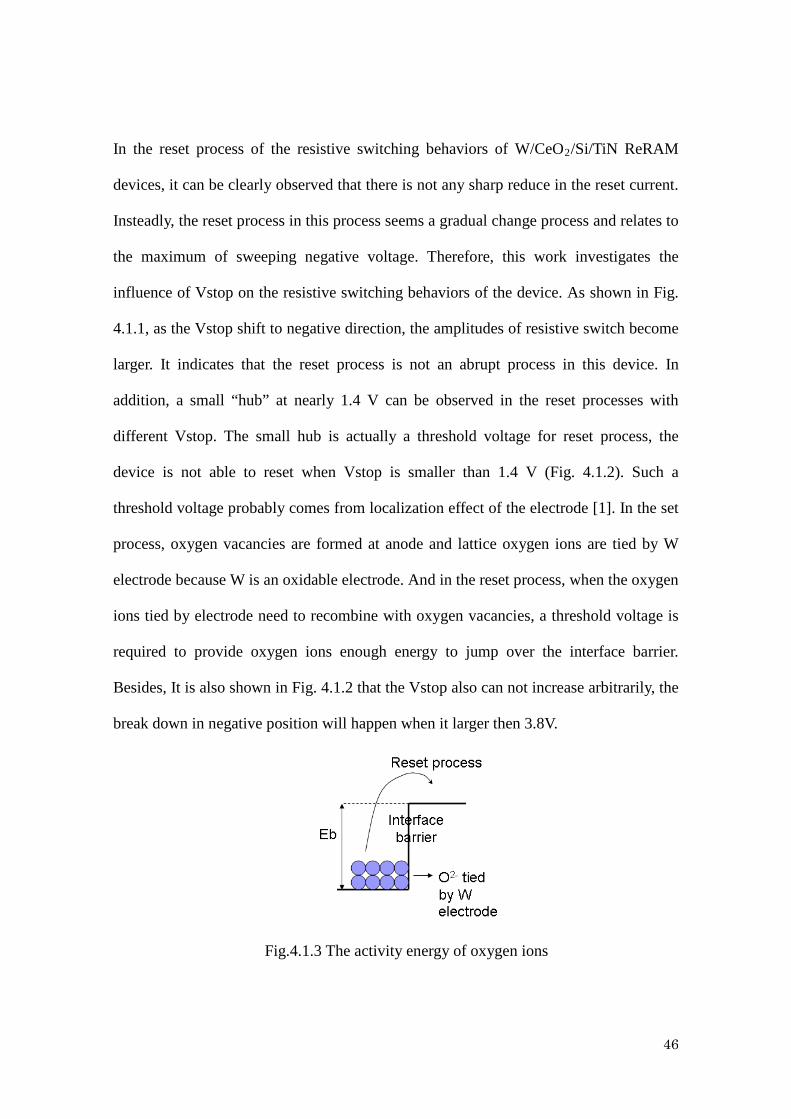
Fig.4.1.2 The reset processes fails at Vstop=3.8V and Vstop=1.4V
Page 46
46
In the reset process of the resistive switching behaviors of W/CeO2/Si/TiN ReRAM
devices, it can be clearly observed that there is not any sharp reduce in the reset current.
Insteadly, the reset process in this process seems a gradual change process and relates to
the maximum of sweeping negative voltage. Therefore, this work investigates the
influence of Vstop on the resistive switching behaviors of the device. As shown in Fig.
4.1.1, as the Vstop shift to negative direction, the amplitudes of resistive switch become
larger. It indicates that the reset process is not an abrupt process in this device. In
addition, a small “hub” at nearly 1.4 V can be observed in the reset processes with
different Vstop. The small hub is actually a threshold voltage for reset process, the
device is not able to reset when Vstop is smaller than 1.4 V (Fig. 4.1.2). Such a
threshold voltage probably comes from localization effect of the electrode [1]. In the set
process, oxygen vacancies are formed at anode and lattice oxygen ions are tied by W
electrode because W is an oxidable electrode. And in the reset process, when the oxygen
ions tied by electrode need to recombine with oxygen vacancies, a threshold voltage is
required to provide oxygen ions enough energy to jump over the interface barrier.
Besides, It is also shown in Fig. 4.1.2 that the Vstop also can not increase arbitrarily, the
break down in negative position will happen when it larger then 3.8V.
Fig.4.1.3 The activity energy of oxygen ions
Page 47
47
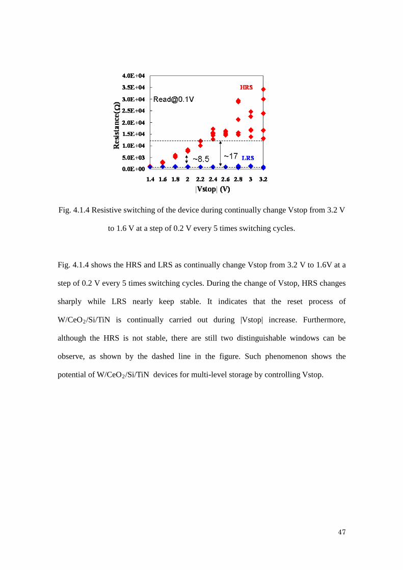
Fig. 4.1.4 Resistive switching of the device during continually change Vstop from 3.2 V
to 1.6 V at a step of 0.2 V every 5 times switching cycles.
Fig. 4.1.4 shows the HRS and LRS as continually change Vstop from 3.2 V to 1.6V at a
step of 0.2 V every 5 times switching cycles. During the change of Vstop, HRS changes
sharply while LRS nearly keep stable. It indicates that the reset process of
W/CeO2/Si/TiN is continually carried out during |Vstop| increase. Furthermore,
although the HRS is not stable, there are still two distinguishable windows can be
observe, as shown by the dashed line in the figure. Such phenomenon shows the
potential of W/CeO2/Si/TiN devices for multi-level storage by controlling Vstop.
Page 48
48
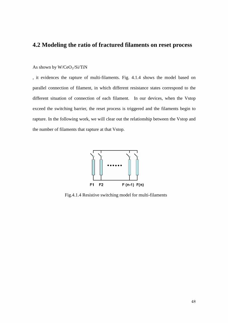
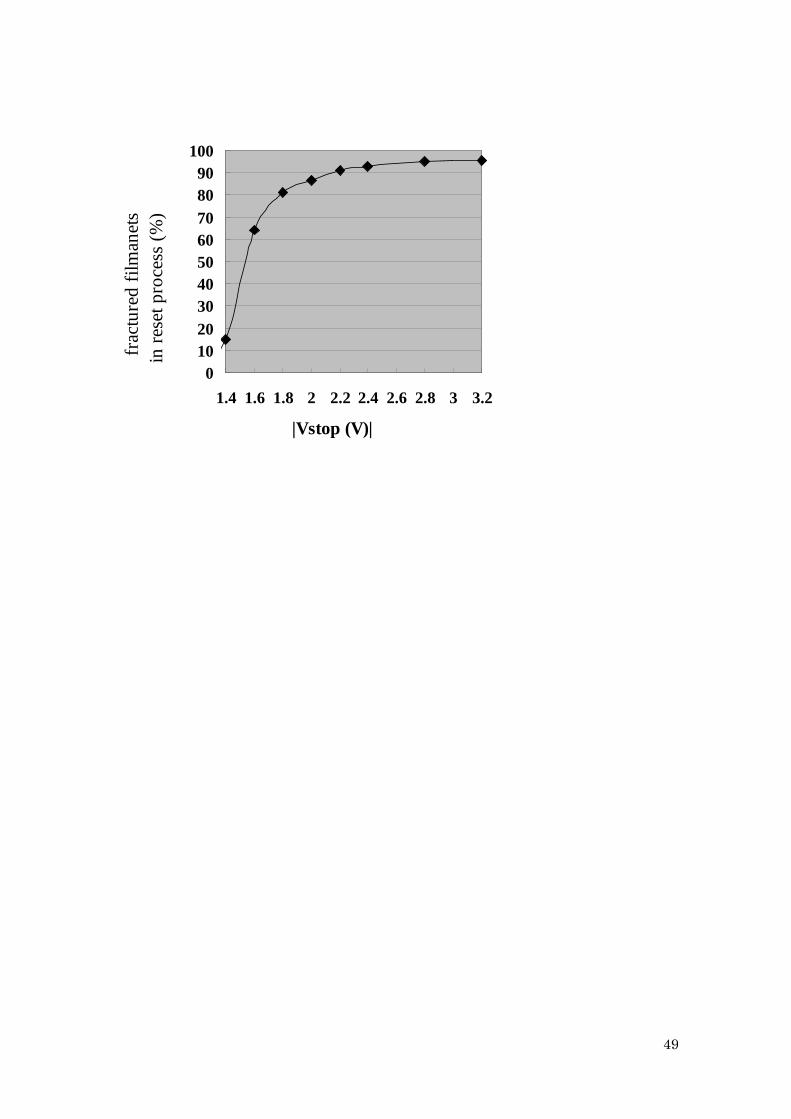
4.2 Modeling the ratio of fractured filaments on reset process
As shown by W/CeO2/Si/TiN
, it evidences the rapture of multi-filaments. Fig. 4.1.4 shows the model based on
parallel connection of filament, in which different resistance states correspond to the
different situation of connection of each filament. In our devices, when the Vstop
exceed the switching barrier, the reset process is triggered and the filaments begin to
rapture. In the following work, we will clear out the relationship between the Vstop and
the number of filaments that rapture at that Vstop.
Fig.4.1.4 Resistive switching model for multi-filaments
Page 49
49
0102030405060708090
100
1.4 1.6 1.8 2 2.2 2.4 2.6 2.8 3 3.2
|Vstop (V)|
frac
ture
d fil
man
ets
in re
set p
roce
ss (%
)
Page 50
50
Chapter 5 Conclusion In this study, a new method for improving the cerium based ReRAM devices by
utilizing Si buffer layer is firstly proposed in consideration of the special characteristics
of CeO2 and Si. Then the ReRAM device having W/CeO2/Si/TiN structure is fabricated
and characterized in detail. Next, by comparison with the device without Si layer
(W/CeO2/TiN), the effect of Si buffer layer is extracted and explained by an model
based on conductive filament mechanism. In addition, the thickness effect of Si buffer
layer is also clarified by experiment results. Lastly, the influence of voltage that applied
during set and reset process on resistive switching behavior of the device is modeled,
which provides a strategy for further improve the device performance. The conclusions
in this work is summarized as following:
1) The ReRAM device having W/CeO2/Si/TiN (and also W/CeO2/TiN) structure
show bipolar resistive switching behaviors, which can be attributed to
conductive filament mechanism in consideration the conductive mechanism and
area dependence of different resistive states.
2) The W/CeO2 (20nm)/Si(1nm)/TiN device has a nearly 30 times big window even
during 60 cycles and also can keep the window longer than 105 s, which is far
more better than that of the device without Si. Besides, the device with Si
doesn’t require a high voltage in forming process and also can work under lower
compliance curret. 3) The effect of Si buffer layer can be explained by following mechanism: The Si
buffer layer reacts with the lattice oxygen ions at the surface of CeO2 and thus
Page 51
51
introduction oxygen vacancies into the interface, which eventually leads to an
easier forming process.
4) Thicker Si buffer layer leads to larger amount of oxygen vacancies and the
thickness of Si buffer layer should be should be optimized to obtain the best
performance of the device. 5) The stage-like HRS caused by continuing change of Vstop evident the existence
of multi-filaments during restive switching process. And rupture of the filaments
is directly related to Vstop.
Page 52
52
Acknoledgement Firstly, I want to express deep gratitude to my supervisor Prof. Hiroshi Iwai at Tokyo
Institute of Technology, who not only offered me a valuable opportunity to start my
graduate study under his guidance, but also always gives me strong support on my
research and life. His spirit of devotion and diligence will always encourage me in
future.
I also would like to sincerely thanks Prof. Takeo Hattori, Prof. Nobuyuki Sugii, Prof.
Kazuo Tsutsui, Assitant Prof. Kuniyuki Kakushima, Assistant Prof. Parhat Ahmet for
their useful advices and patient help since I came here.
I also want to appreciate the research colleagues of Professor Iwai’s laboratory members.
They help me a lot in the dairy research and life.
Besides, special thanks to laboratory secretaries, Ms A. Matsumoto, Ms. M. Nishizawa,
and also Ms. M. Karakawa.
And also, I would also like to thanks my parents, and all of my family members, for
their always warm support.
Finally, acknowledgements to the Ministry of Education, Culture, Sport, Science and
Technology, Government of Japan for offering me Monbukagakusho scholarship during
my master course.
Chunmeng Dou
January 2010