Communications on Applied Electronics (CAE) – ISSN : 2394-4714 Foundation of Computer Science FCS, New York, USA Volume 3– No.2, October 2015 – www.caeaccess.org 27 Constructing Complete Radio Frequency Receiver for LTE TDD Transceiver Dalia Sadek Ain shams university Cairo - Egypt Heba A. Shawkey Electronics Research Institute (ERI) Giza – Egypt Abdelhalim Zekry Ain shams university Cairo - Egypt ABSTRACT In this paper, the design, implementation and testing of the Zero IF receiver for Long Term Evolution (LTE) band 36 extending from 1930MHz to 1990MHz for TDD mode of transmission. Comprising a passive part and active part. The passive part consists of a microstrip patch antenna and a Hairpin BPF filter which are fabricated with a total area of 43x36mm 2 for the antenna and 38.6x32.16mm 2 for the filter. The proposed devices are fabricated using FR-4 material substrate with dielectric constant of Ɛr=4.4, thickens h =1.6, and Loss tangent of 0.025. The active part includes Low noise amplifier, IQ demodulator and frequency synthesizer. Which are a real made component selected off-shelf to satisfy the standards for LTE receiver characteristics. The proposed RF front-end receiver achieves a 4.022 dB NF, 2.65 dBm IIP3. Keywords LTE, TDD, band 36, Zero IF receiver, Micro-strip, Patch antenna, filter, FR-4 material, LNA, Frequency Synthesizer and Demodulator 1. INTRODUCTION LTE is the abbreviation for Long Term Evolution [1] and is the trademark owned by ETSI (European Telecommunications Standards Institute) for the wireless data communications technology and a development of the GSM/UMTS standards. However, many companies do play an active role in the LTE project. A new DSP (digital signal processing) techniques and modulations that were developed around the turn of the millennium were used to increase the capacity and speed of wireless data network which is the main goal of the LTE. An additional goal was the redesign and simplification of the network architecture to an IP-based system with significantly reduced transfer latency compared to the 3G architecture [2]. The downlink capacity of at least 300 Mbps and uplink capacity of at least 75Mbps. LTE supports both frequency division duplex (FDD) and time-division duplex (TDD). The LTE can use QPSK, 16QAM or 64QAM modulation schemes. It supports six different channel bandwidths: 1.4MHz, 3MHz, 5MHz, 10MHz, 15MHz, and 20MHz [3]. In that respect are several existing plans and implementations that have been described in the literature. Such as 1900 Direct Conversion Receiver using 0.13μm CMOS in [4]. A front-end for LTE direct conversion SAW-less receiver using A 1.2-V CMOS in [5]. A WiMAX/LTE receiver front-end using 90 NM CMOS in [6]. Based on our knowledge, it is the first time to introduce a design and implementation of the whole LTE RF receiver which consists of an antenna, band pass filter, Low noise amplifier, IQ demodulator, and frequency synthesizer for LTE band 2 FDD or band 36 TDD. The paper is organized as follows; section 2 presents the receiver architecture and key parameters, section 3 the passive front end for LTE receiver, section 4 the active front end for the LTE receiver section 5 measurements of the whole RF receiver finally, section 6 is for conclusion. 2. RECEIVER ARCHITECTURES AND KEY PARAMETERS The function of a receiver is to successfully demodulate a desired signal in the presence of strong interference and noise [7]. A receiver system needs to minimize cost and power consumption a number of different requirements translate into different receiver architectures. The development towards small size and low cost integrated circuits with a higher degree of components, integrated on the chip has made the simple architecture of the Zero IF receiver architectures. The proposed RF receiver (Zero IF architecture) shown in figure 1. The main parts of the RF receiver are the following: 1. Antenna: E-Shape patch antenna operates 1903.2 MHz to 2011MHz, BW 107.7 MHz, at return loss - 6 dB, minimum return loss -28.58 dB this antenna covers LTE TDD frequency band 36. 2. Band-pass filter (BPF): The designed and implemented Hairpin filter operates at the center frequency 1950 MHz and 90 MHz BW at 3 dB. 3. Low-noise amplifier (LNA): The selected RF Low Noise Amplifier (RF2442) has Low Noise, High Intercept and 500MHz to 2500MHz Operation. The LNA achieves gain of about 12 dB at the operating frequency 1.95 GHz and Vcc=3.6 V. 4. Local oscillator (LO): The frequency synthesizer is selected (LTC 6949) with step size of 200 KHz and frequency range from 0.37GHz to 5.7GHz, so that it covers all LTE bands. 5. The mixer: The selected direct conversion I/Q demodulator (LTC 5585) has a frequency range from 0.7GHz to 3GHz.The RF signal is directly converted into I and Q baseband signals. With
Transcript
Communications on Applied Electronics (CAE) – ISSN : 2394-4714
Foundation of Computer Science FCS, New York, USA
Volume 3– No.2, October 2015 – www.caeaccess.org
27
Constructing Complete Radio Frequency Receiver for LTE TDD Transceiver
Dalia Sadek
Ain shams university Cairo - Egypt
Heba A. Shawkey Electronics Research Institute
(ERI) Giza – Egypt
Abdelhalim Zekry Ain shams university
Cairo - Egypt
ABSTRACT
In this paper, the design, implementation and testing of the
Zero IF receiver for Long Term Evolution (LTE) band 36
extending from 1930MHz to 1990MHz for TDD mode of
transmission. Comprising a passive part and active part. The
passive part consists of a microstrip patch antenna and a
Hairpin BPF filter which are fabricated with a total area of
43x36mm2 for the antenna and 38.6x32.16mm2 for the filter.
The proposed devices are fabricated using FR-4 material
substrate with dielectric constant of Ɛr=4.4, thickens h =1.6,
and Loss tangent of 0.025.
The active part includes Low noise amplifier, IQ
demodulator and frequency synthesizer. Which are a real
made component selected off-shelf to satisfy the standards
for LTE receiver characteristics.
The proposed RF front-end receiver achieves a 4.022 dB NF,
2.65 dBm IIP3.
Keywords LTE, TDD, band 36, Zero IF receiver, Micro-strip,
Patch antenna, filter, FR-4 material, LNA, Frequency
Synthesizer and Demodulator
1. INTRODUCTION LTE is the abbreviation for Long Term Evolution [1] and is
the trademark owned by ETSI (European
Telecommunications Standards Institute) for the wireless
data communications technology and a development of the
GSM/UMTS standards. However, many companies do play
an active role in the LTE project. A new DSP (digital signal
processing) techniques and modulations that were developed
around the turn of the millennium were used to increase the
capacity and speed of wireless data network which is the
main goal of the LTE. An additional goal was the redesign
and simplification of the network architecture to an IP-based
system with significantly reduced transfer latency compared
to the 3G architecture [2]. The downlink capacity of at least
300 Mbps and uplink capacity of at least 75Mbps.
LTE supports both frequency division duplex (FDD) and
time-division duplex (TDD). The LTE can use QPSK,
16QAM or 64QAM modulation schemes. It supports six
different channel bandwidths: 1.4MHz, 3MHz, 5MHz,
10MHz, 15MHz, and 20MHz [3].
In that respect are several existing plans and implementations
that have been described in the literature. Such as 1900
Direct Conversion Receiver using 0.13µm CMOS in [4]. A
front-end for LTE direct conversion SAW-less receiver using
A 1.2-V CMOS in [5]. A WiMAX/LTE receiver front-end
using 90 NM CMOS in [6]. Based on our knowledge, it is
the first time to introduce a design and implementation of the
whole LTE RF receiver which consists of an antenna, band
pass filter, Low noise amplifier, IQ demodulator, and
frequency synthesizer for LTE band 2 FDD or band 36 TDD.
The paper is organized as follows; section 2 presents the
receiver architecture and key parameters, section 3 the
passive front end for LTE receiver, section 4 the active front
end for the LTE receiver section 5 measurements of the
whole RF receiver finally, section 6 is for conclusion.
2. RECEIVER ARCHITECTURES AND
KEY PARAMETERS The function of a receiver is to successfully demodulate a
desired signal in the presence of strong interference and
noise [7].
A receiver system needs to minimize cost and power
consumption a number of different requirements translate
into different receiver architectures. The development
towards small size and low cost integrated circuits with a
higher degree of components, integrated on the chip has
made the simple architecture of the Zero IF receiver
architectures. The proposed RF receiver (Zero IF
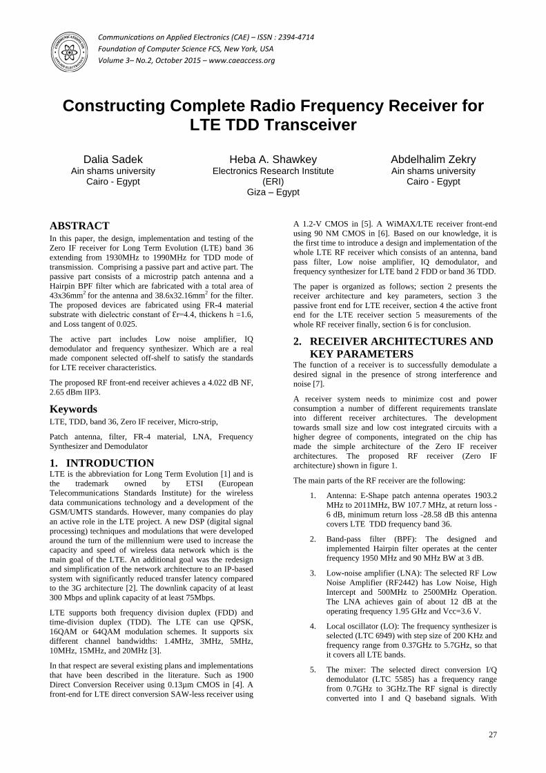
architecture) shown in figure 1.
The main parts of the RF receiver are the following:
1. Antenna: E-Shape patch antenna operates 1903.2
MHz to 2011MHz, BW 107.7 MHz, at return loss -
6 dB, minimum return loss -28.58 dB this antenna
covers LTE TDD frequency band 36.
2. Band-pass filter (BPF): The designed and
implemented Hairpin filter operates at the center
frequency 1950 MHz and 90 MHz BW at 3 dB.
3. Low-noise amplifier (LNA): The selected RF Low
Noise Amplifier (RF2442) has Low Noise, High
Intercept and 500MHz to 2500MHz Operation.
The LNA achieves gain of about 12 dB at the
operating frequency 1.95 GHz and Vcc=3.6 V.
4. Local oscillator (LO): The frequency synthesizer is
selected (LTC 6949) with step size of 200 KHz and
frequency range from 0.37GHz to 5.7GHz, so that
it covers all LTE bands.
5. The mixer: The selected direct conversion I/Q
demodulator (LTC 5585) has a frequency range
from 0.7GHz to 3GHz.The RF signal is directly
converted into I and Q baseband signals. With
Communications on Applied Electronics (CAE) – ISSN : 2394-4714
Foundation of Computer Science FCS, New York, USA
Volume 3– No.2, October 2015 – www.caeaccess.org
28
Conversion Gain 2.4 dB at 1950 MHz.
The key parameters to measure for the receiver are the
receiver Noise Figure, The receiver sensitivity, the
receiver Dynamic range and the receiver linearity.
Fig 1: The proposed zero if receiver topology
3. PASSIVE FRONT END FOR LTE
RECEIVER Micro-strip technics are used for the passive part (the
antenna and the band pass filter). The detailed description
passive front end is given in [8]
3.1 LTE Antenna Design Figure 2 (a) and (b) shows the top and bottom views of the
design of the proposed antenna whose dimensions are
determined with the help of CST simulator and listed in
Table 1 [8].
Fig 2: Antenna Design (a) Top view (b) Bottom
view
Table 1. Antenna parameter’s size
Parameter Size(mm) Parameter Size(mm)
Ls 43 LD 28
Ws 36 Li 6.6
Lp 27.5 Wi 1.25
Wp 24 WB 13.57
Lf 18.5 LB 2.45
Wf 2.97 LA 4.05
The antenna is then fabricated and its photographs are shown
in Figure 3 (a) and (b)
Fig 3: Antenna photography (a) Top view (b) Bottom
view
Figure 4 demonstrates the return loss (S-Parameter) value, as
a result of antenna simulation and antenna measurement.
From the antenna simulation the antenna operates between
1903.3 MHz and 2011.1 MHz with Bandwidth 107.7 MHz at
return loss -6 dB, minimum return loss -28.58 dB this
antenna covers LTE TDD frequency band 36 [8].
Fig 4: Comparison between the simulation and measured
Communications on Applied Electronics (CAE) – ISSN : 2394-4714
Foundation of Computer Science FCS, New York, USA
Volume 3– No.2, October 2015 – www.caeaccess.org
29
results for the antenna
(a) (b)
Fig 5: Filter Design (a) Top view (b) Filter photography
3.2 LTE Filter Design The filter is designed and simulated using the CST simulator
program Figure 5 (a) and (b) shows Filter design Top view
and the photograph of its fabrication. The dimensions are
given in Table 2 [8].
Table 2. Filter parameter’s size
Parameter Size(mm) Parameter Size(mm)
L 38.6 E 3.8
W 32.16 H 3.2
A 36.6 G 4
B 2 F 11.2
C 7.8 t 0.38
The simulated performance of the filter is shown in Figure 6.
From the measurements, the -3dB BW of the filter amounts
to 90 MHZ and a center frequency of 1950MHz. It is clear
from the figure that there is a satisfactory agreement between
the simulated and measured results [8].
Fig 6: Comparison between the simulation and measured
results for the Hairpin filter
4 ACTIVE FRONT END The active components of Zero IF Architectures consist of
Low noise amplifier, demodulator and synthesizer, which are
real made components were selected off-shelf from different
types and different companies to satisfy the specifications
required for the proposed LTE front end receiver. Here also,
their performance parameters are verified by intensive RF
measurements.
4.2 Low Noise Amplifier (LNA)
The first component in the active front end is the LNA. It
amplifies the received signals to acceptable levels with
minimum self-generated additional noise. It is usually
located very close to the Antenna [9] to reduce losses in the
feed-line. LNA is a design that minimizes the noise figure of
the system by matching the device to its noise matching
impedance [10].
RF2442 is the selected low noise amplifier. It has a very high
dynamic range designed for front end receiver for digital
cellular applications and covers all bands of LTE from 500
MHz to 2500 MHz. According to the data sheet, its
performance parameters are outlined as follows:
The DC power consumption is a major parameter in the
LNA. RF2442 operates from 3.6 V power supply and
consumes about 0.23 W. The measured S-parameters of the
amplifier as a function of frequency is shown in Fig. 7. The
frequency range is that of LTE from 1930MHz to1980MHz.
Gain (dB) = 10log (Pout/Pin) = S21 (dB)
It is clear from the figure that, at the center Frequency 1950
MHz, the Gain S21=12.126 dB, the Return losses at the input
and output respectively, S11 = -15 dB, and S22 = -12.5 dB,
and the Reverse isolation S12 = - 20 dB
Fig 7: LNA S-parameters (dB) measurement
For the measurement of the one dB compression point P1-dB
of the LNA, the input power is changed and the
corresponding output power at 1950 MHz is measured and
the results are plotted in Figure 8.
Fig 8: 1dB compression point at 1950MHz
From the curve, the Output P1dB =15.6dBm. One can
Communications on Applied Electronics (CAE) – ISSN : 2394-4714
Foundation of Computer Science FCS, New York, USA
Volume 3– No.2, October 2015 – www.caeaccess.org
30
calculate the third intercept point of the amplifier IP3 use the
formula: Output at IP3 ~output at P1dB + 11dB [11], which
results in Output IP3~26.6dBm.
4.3 Frequency Synthesizer The second component in the active front end is the
frequency synthesizer. It is an electronic system for
generating any of a range of frequencies from a single fixed
time base or oscillator. A frequency synthesizer can combine
frequency to produce the desired output signal [12].
The LTC6946 is the selected Frequency synthesizer for the
proposed LTE RF receiver. It has high performance, low
noise, phase-locked loop (PLL) with a fully integrated VCO,
including a reference divider, phase-frequency detector
(PFD) with phase-lock indicator, ultra-low noise charge
pump, integer feedback divider, and VCO output divider.
Figure 10 shows a simplified LTC6946 block diagram, with
the external loop filter components. The phase/frequency
detector (PFD) compares the phase and frequency of the
reference clock fREF, after dividing it by R to produce fPFD,
for those of the VCO following an integer division of N. The
PFD, then controls the current sources of the charge pump to
ensure that the VCO runs at a rate such that when it is
divided by N, its frequency is equal to fPFD and its phase is in
sync with the reference clock. This describes a negative
feedback mechanism, with the external loop filter
components stabilizing the loop and setting the control
bandwidth. The O divider increases the output frequency
range by dividing down the VCO output to create more
frequency bands than just that of the VCO.
Fig 9: Simplified LTC6946 block diagram [13]
When the loop is locked, the frequency fVCO (in Hz)
produced at the output of the VCO is determined by the
reference frequency, fREF, and the R and N divider values,
according to:
fVCO =fREF ∗N
R (1)
The PFD frequency fPFD is given by:
fPFD =fREF
R (2)
FVCO may be alternatively expressed as
fVCO = fPFD ∗ N (3)
The output frequency fRF produced at the output of the O
divider is given by
fRF =fVCO
O (4)
Using the above equations, the output frequency resolution
fSTEP produced by a unit change in N is given by
fSTEP =fREF
R∗O (5)
Figure 10 shows the setup for measuring the frequency
synthesizer board where it is connected to power supplies 5v
and 3.3v, a DC590 controller board connected to PC USB
port to operate it under control of PLL wizard software in a
personal computer, a reference frequency source and the RF
output is connected to the spectrum analyzer. The frequency
of the frequency synthesizer is set by the wizard software via
the DC590 USB serial controller board. Figure 11 shows the wizard adjusted such that:
LO frequency band: 1920 MHz to 1980 MHz
Frequency step size (channel-to-channel
spacing):20MHz
Reference clock frequency: 10 MHz
The LTC6946 VCO gain is nearly constant as a percentage
of the frequency so the loop filter designed at any frequency
within the band works for all other frequencies.
Fig 10: Measurement setup of DC1705B frequency
synthesizer
Fig 11: Loop Filter Design for PLLWizard software at
frequency 1940 MHZ
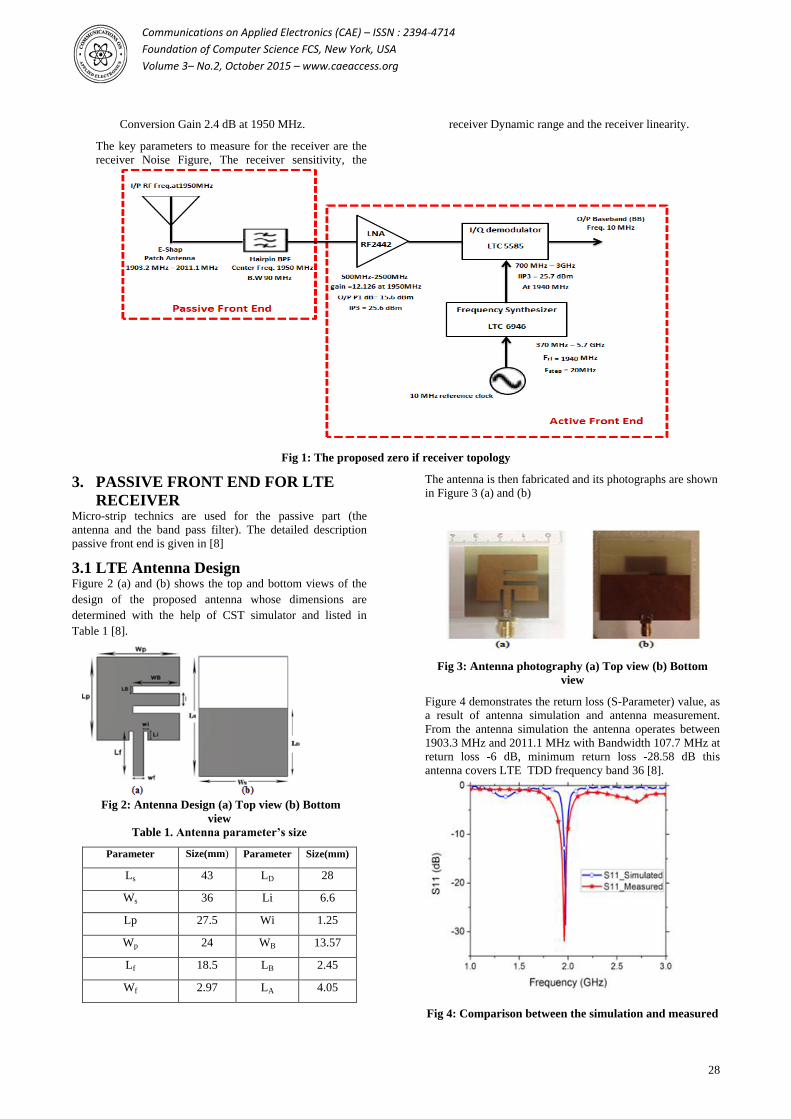
Figure 12 shows the output of the synthesizer on the screen
of the spectrum analyzer. It is clear from the figure that the
synthesizer output frequency amounts to 1940 MHz at an
output power level of 0 dBm.
Communications on Applied Electronics (CAE) – ISSN : 2394-4714
Foundation of Computer Science FCS, New York, USA
Volume 3– No.2, October 2015 – www.caeaccess.org
31
Fig 12: The RF output of the Frequency Synthesizer at
frequency 1940 MHz
4.4 The Direct Conversion I/Q
Demodulator The third and last building block in the active front end is the
IQ demodulator for direct frequency conversion, allowing a
receiver to demodulate the wide RF signal directly to
baseband [14].
The chip LTC5585 is selected to function as a direct
conversion quadrature demodulator for the proposed RF
receiver. It is suitable for communication receivers where an
RF signal is directly converted into I and Q baseband signals
with bandwidth of 530MHz or higher. The LTC5585
incorporates balanced I and Q mixers, LO buffer amplifiers
and a precision, high frequency quadrature phase shifter. The
integrated on-chip broadband transformer provides a single-
ended interface at the RF input with a simple off-chip L-C
matching. In addition, the LTC5585 provides four analog
control voltage interface pins for IIP2 and DC offset
correction, greatly simplifying system calibration. The high
linearity of the LTC5585 provides excellent spurfree
dynamic range of the receiver. These I/Q outputs can
interface directly to channel-select filters (LPFs) or to
baseband amplifiers.
Demonstration circuit DC1662 is designed for evaluating the
LTC5585 IC at RF frequencies from 700MHz to 3GHz, with
a supply voltage range from 0.3V to 5.5V, and about 250mA
current.
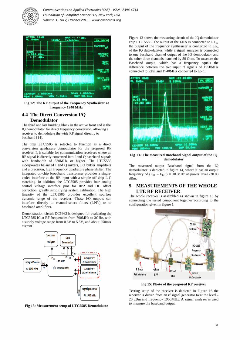
Fig 13: Measurement setup of LTC5585 Demodulator
Figure 13 shows the measuring circuit of the IQ demodulator
chip LTC 5585. The output of the LNA is connected to RFin,
the output of the frequency synthesizer is connected to Loin
of the IQ demodulator, while a signal analyzer is connected
to one baseband channel output of the IQ demodulator and
the other three channels matched by 50 Ohm. To measure the
Baseband output, which has a frequency equals the
difference between the two input rf signals of 1950MHz
connected to RFin and 1940MHz connected to Loin.
Fig 14: The measured Baseband Signal output of the IQ
demodulator
The measured output Baseband signal from the IQ
demodulator is depicted in figure 14, where it has an output
frequency of (FRF – FLO ) = 10 MHz at power level -20.83
dBm.
5 MEASUREMENTS OF THE WHOLE
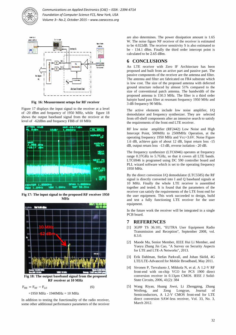
LTE RF RECEIVER The whole receiver is assembled as shown in figure 15 by
connecting the tested component together according to the
configuration given in figure 1.
Fig 15: Photo of the proposed RF receiver
Testing setup of the receiver is depicted in Figure 16 the
receiver is driven from an rf signal generator to at the level -
20 dBm and frequency 1950MHz. A signal analyzer is used
to measure the baseband output.
Communications on Applied Electronics (CAE) – ISSN : 2394-4714
Foundation of Computer Science FCS, New York, USA
Volume 3– No.2, October 2015 – www.caeaccess.org
32
Fig 16: Measurement setups for RF receiver
Figure 17 displays the input signal to the receiver at a level
of -20 dBm and frequency of 1950 MHz, while figure 18
shows the output baseband signal from the receiver at the
level of -62dBm and frequency FBB of 10 MHz
Fig 17: The input signal to the proposed RF receiver 1950
MHz
Fig 18: The output baseband signal from the proposed
RF receiver at 10 MHz
FBB = FRF − FLO (6)
=1950 MHz - 1940MHz = 10 MHz
In addition to testing the functionality of the radio receiver,
some other additional performance parameters of the receiver
are also determines. The power dissipation amount is 1.65
W. The noise figure NF receiver of the receiver is estimated
to be 4.022dB. The receiver sensitivity S is also estimated to
be - 134.1 dBm. Finally the third order intercept point is
calculated to be 2.65 dBm.
6 CONCLUSIONS An LTE receiver with Zero IF Architecture has been
proposed and built from an active part and passive part. The
passive components of the receiver are the antenna and filter.
The antenna and filter are fabricated on FR4 substrate which
is low cost. The size of the proposed antenna with defected
ground structure reduced by almost 51% compared to the
size of conventional patch antenna. The bandwidth of the
proposed antenna is 150.3 MHz. The filter is a third order
hairpin band pass filter at resonant frequency 1950 MHz and
3 dB frequency 90 MHz.
The active elements include low noise amplifier, I/Q
demodulator and frequency synthesizer. They are selected
from off-shelf components after an intensive search to satisfy
the requirements of the front end LTE receiver.
RF low noise amplifier (RF2442) Low Noise and High
Intercept Point, 500MHz to 2500MHz Operation, at the
operating frequency 1950 MHz and Vcc=3.6V. Noise Figure
1.6 dB, achieve gain of about 12 dB, Input return loss -15