0885-8993 (c) 2016 IEEE. Personal use is permitted, but republication/redistribution requires IEEE permission. See http://www.ieee.org/publications_standards/publications/rights/index.html for more information. This article has been accepted for publication in a future issue of this journal, but has not been fully edited. Content may change prior to final publication. Citation information: DOI 10.1109/TPEL.2016.2570429, IEEE Transactions on Power Electronics 1 Control Concepts for Hybrid Rectifiers Utilizing a Flying Converter Cell Active Current Injection Unit Markus Makoschitz, Student Member, IEEE, Michael Hartmann, Member, IEEE, and Hans Ertl, Member, IEEE Abstract—A passive three-phase rectifier circuit equipped with a ”Flying Converter Cell” (FCC) active current shaping net- work, based on the third harmonic injection concept, has been introduced recently. This additional/optional circuit allows the upgrade of a standard B6 diode rectifier to a low harmonic input stage with unity power factor. In order to guarantee properly shaped sinusoidal mains input currents, dedicated current and voltage controllers of the active circuitry must be designed carefully. As the active current injection unit consists of an assembly of 3 individual converter stages, the design procedure of both current and superimposed voltage controllers results in fairly high complexity. It is therefore going to be discussed in detail in this work. Based on the analysis of the rectifier system an appropriate control concept is developed which is implemented using a digital signal processor. It is furthermore shown that the midpoint voltage of the FCC can advantageously be used for balancing of the DC capacitor stage of the cell without deteriorating THD of mains input currents. Measurement results taken from a 10 kW/10 kHz laboratory prototype finally confirm promising characteristics of the total hybrid system. Index Terms—Three-Phase AC-DC Conversion, Third- Harmonic Injection, Current Control, Voltage Control, Voltage Balancing, Input Current Quality, I. I NTRODUCTION In times of increasing power demand, active three-phase rectifier circuits are gaining more and more importance dur- ing the last decades. Especially applications as e.g. switch- mode power supplies and AC drives where increasingly (i) low harmonic input/line currents (THD i < 5%), (ii) high power factor (λ> 0.99) and (iii) high efficiency (η> 95%) are mandatory ([1]), are of major concern. Numerous active rectifiers (as e.g. the Vienna Rectifier [2])) have been reported in literature which can achieve the mentioned requirements. Purely active rectifier systems, as e.g. the six-switch (active) rectifier, are state-of-the-art circuits for low voltage mains applications. Due to simplicity, robustness and low complexity the six-switch rectifier is widely used in industry and active components are available as combined power modules from numerous manufacturers. This topology however results in large volume of input inductors and shows limited maximum switching frequency (mentioned in [3]). The derived three- level topologies (i.e. NPC or T-Type) are characterised by reduced volume of passive components, lower switching losses and reduced voltage stress of switching devices. However, the mentioned topologies suffer from higher conduction losses and Markus Makoschitz and Hans Ertl are with the Institute of Energy Systems and Electrical Drives (Power Electronics Section), Vienna University of Technology, Vienna 1040, Austria (e-mail: [email protected], [email protected]). Michael Hartmann is with Schneider Electric, Technology Center, Power Drives, Vienna 1210, Austria (e-mail: [email protected]). increased complexity compared to a two-level implementation. Active switching components of all these mentioned topolo- gies, however, have to process the full active power. This issue can be reduced or overcome by some specific hybrid rectifiers which are only stressed by a small amount of active and reactive power. Hybrid rectifiers e.g. employing third harmonic injection cir- cuits (consisting of an active current shaping cell and an active current injection unit) can be separated into (i) active cur- rent injection/active current shaping (ii) passive current injec- tion/active current shaping (iii) active current injection/passive current shaping (iv) passive current injection/passive current shaping. [4]–[18] mention different types of rectifier topologies ap- plying the third harmonic injection principle whereas passive current injection/active current shaping is assumed. [4]–[8] and [10]–[13] discuss two different versions of the Minnesota rectifier. The first solution discloses DC-side located boost converter stages with additional passive third harmonic injec- tion network. It can be implemented as series connected LC circuit, which is tuned close to the 3 rd harmonic frequency. The second version considers a buck converter stage at the out- put of the rectifier, followed by a boost topology. The current injection network consists of a zig-zag transformer, which is connecting the injection path to each phase. These topologies, however, cannot serve as optional upgrade of passive three- phase rectifiers. Furthermore, both DC-DC converters have to process the main part of the active power. Hybrid rectifiers as discussed in [19]–[26] are classified by passive current injection/passive current shaping. In [22], the current injection network is implemented as simple and very well known star/delta transformer (whereas the secondary side of the transformer is short-circuited) and constitutes the interconnection between the AC- and the DC-side of the passive diode bridge rectifier topology. The third harmonic current is generated according to the instantaneous state of the passive rectifier and the design of the implemented passive components. A total harmonic input current distortion of < 5% is achievable if the ratio between third harmonic current i f and output current I o is close or equal to 1 (= i f /I o ). This can be accomplished e.g. by the use of a saturable reactor or a magnetic amplifier which however results in unfavorable complexity of the circuit. A rectifier option considering active current injection/passive current shaping is explained in [25]. The proposed topology is an extension circuitry for three-phase diode bridge rectifiers consisting of an active current injection network (implemented as bidirectional switch arrangement) and a passive current shaping network (composed of 3 resistors and 2 capaci-
Transcript
0885-8993 (c) 2016 IEEE. Personal use is permitted, but republication/redistribution requires IEEE permission. See http://www.ieee.org/publications_standards/publications/rights/index.html for more information.
This article has been accepted for publication in a future issue of this journal, but has not been fully edited. Content may change prior to final publication. Citation information: DOI 10.1109/TPEL.2016.2570429, IEEETransactions on Power Electronics
1
Control Concepts for Hybrid Rectifiers Utilizing aFlying Converter Cell Active Current Injection UnitMarkus Makoschitz, Student Member, IEEE, Michael Hartmann, Member, IEEE, and Hans Ertl, Member, IEEE
Abstract—A passive three-phase rectifier circuit equipped witha ”Flying Converter Cell” (FCC) active current shaping net-work, based on the third harmonic injection concept, has beenintroduced recently. This additional/optional circuit allows theupgrade of a standard B6 diode rectifier to a low harmonic inputstage with unity power factor. In order to guarantee properlyshaped sinusoidal mains input currents, dedicated current andvoltage controllers of the active circuitry must be designedcarefully. As the active current injection unit consists of anassembly of 3 individual converter stages, the design procedureof both current and superimposed voltage controllers results infairly high complexity. It is therefore going to be discussed indetail in this work. Based on the analysis of the rectifier system anappropriate control concept is developed which is implementedusing a digital signal processor. It is furthermore shown thatthe midpoint voltage of the FCC can advantageously be usedfor balancing of the DC capacitor stage of the cell withoutdeteriorating THD of mains input currents. Measurement resultstaken from a 10 kW/10 kHz laboratory prototype finally confirmpromising characteristics of the total hybrid system.
Index Terms—Three-Phase AC-DC Conversion, Third-Harmonic Injection, Current Control, Voltage Control, VoltageBalancing, Input Current Quality,
I. INTRODUCTION
In times of increasing power demand, active three-phaserectifier circuits are gaining more and more importance dur-ing the last decades. Especially applications as e.g. switch-mode power supplies and AC drives where increasingly (i)low harmonic input/line currents (THDi < 5%), (ii) highpower factor (λ > 0.99) and (iii) high efficiency (η > 95%)are mandatory ([1]), are of major concern. Numerous activerectifiers (as e.g. the Vienna Rectifier [2])) have been reportedin literature which can achieve the mentioned requirements.Purely active rectifier systems, as e.g. the six-switch (active)rectifier, are state-of-the-art circuits for low voltage mainsapplications. Due to simplicity, robustness and low complexitythe six-switch rectifier is widely used in industry and activecomponents are available as combined power modules fromnumerous manufacturers. This topology however results inlarge volume of input inductors and shows limited maximumswitching frequency (mentioned in [3]). The derived three-level topologies (i.e. NPC or T-Type) are characterised byreduced volume of passive components, lower switching lossesand reduced voltage stress of switching devices. However, thementioned topologies suffer from higher conduction losses and
Markus Makoschitz and Hans Ertl are with the Institute of Energy Systemsand Electrical Drives (Power Electronics Section), Vienna University ofTechnology, Vienna 1040, Austria (e-mail: [email protected],[email protected]).
Michael Hartmann is with Schneider Electric, Technology Center, PowerDrives, Vienna 1210, Austria (e-mail: [email protected]).
increased complexity compared to a two-level implementation.Active switching components of all these mentioned topolo-gies, however, have to process the full active power. Thisissue can be reduced or overcome by some specific hybridrectifiers which are only stressed by a small amount of activeand reactive power.Hybrid rectifiers e.g. employing third harmonic injection cir-cuits (consisting of an active current shaping cell and an activecurrent injection unit) can be separated into (i) active cur-rent injection/active current shaping (ii) passive current injec-tion/active current shaping (iii) active current injection/passivecurrent shaping (iv) passive current injection/passive currentshaping.[4]–[18] mention different types of rectifier topologies ap-plying the third harmonic injection principle whereas passivecurrent injection/active current shaping is assumed. [4]–[8]and [10]–[13] discuss two different versions of the Minnesotarectifier. The first solution discloses DC-side located boostconverter stages with additional passive third harmonic injec-tion network. It can be implemented as series connected LCcircuit, which is tuned close to the 3rd harmonic frequency.The second version considers a buck converter stage at the out-put of the rectifier, followed by a boost topology. The currentinjection network consists of a zig-zag transformer, which isconnecting the injection path to each phase. These topologies,however, cannot serve as optional upgrade of passive three-phase rectifiers. Furthermore, both DC-DC converters have toprocess the main part of the active power.Hybrid rectifiers as discussed in [19]–[26] are classified bypassive current injection/passive current shaping. In [22],the current injection network is implemented as simple andvery well known star/delta transformer (whereas the secondaryside of the transformer is short-circuited) and constitutes theinterconnection between the AC- and the DC-side of thepassive diode bridge rectifier topology. The third harmoniccurrent is generated according to the instantaneous state ofthe passive rectifier and the design of the implemented passivecomponents. A total harmonic input current distortion of < 5%is achievable if the ratio between third harmonic current ifand output current Io is close or equal to 1 (= if/Io). Thiscan be accomplished e.g. by the use of a saturable reactoror a magnetic amplifier which however results in unfavorablecomplexity of the circuit.A rectifier option considering active current injection/passivecurrent shaping is explained in [25]. The proposed topologyis an extension circuitry for three-phase diode bridge rectifiersconsisting of an active current injection network (implementedas bidirectional switch arrangement) and a passive currentshaping network (composed of 3 resistors and 2 capaci-
0885-8993 (c) 2016 IEEE. Personal use is permitted, but republication/redistribution requires IEEE permission. See http://www.ieee.org/publications_standards/publications/rights/index.html for more information.
This article has been accepted for publication in a future issue of this journal, but has not been fully edited. Content may change prior to final publication. Citation information: DOI 10.1109/TPEL.2016.2570429, IEEETransactions on Power Electronics
2
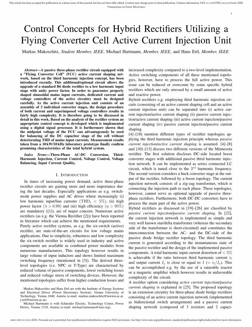
Fig. 1: Active three-phase rectifier circuit utilizing a ”Flying” converter cellas proposed in [27] and [28].
tors). The system shows promising results for nominal load,however, appears to be inefficient for partial and light loadoperation.On the contrary, hybrid rectifiers with active current injec-tion/active current shaping (as proposed and/or discussedin [29]–[40]) serve as promising solutions to guarantee lowharmonic input currents and a high power factor. All of theserectifiers are characterized by different attributes. Therefore,the proper selection of one specific rectifier highly dependson the given application, specifications and requirements (e.g.controllable output voltage buck - [32], controllable outputvoltage boost - [33], [34], upgradeable B6 rectifier - [35]–[38] (dependent on passive topology - e.g. AC-side, DC-side smoothing inductor) etc.). Another opportunity would beto apply flying capacitor converters on the AC-side of thesystem (as e.g. described in [41]). These rectifiers are ableto provide bidirectional power flow. The FCC as described inthis work is however only able to allow unidirectional powerflow (predetermined due to the B6 rectifier topology). It hasto be mentioned, that low harmonic input currents and unitypower factor can also be achieved, if the active current shapingnetwork is implemented as two flying capacitor converterbranches in back-to-back connection. However, it must beconsidered, that each capacitor stage has to process 150 Hz and300 Hz current components which leads to a relatively largecapacitor volume (at least 4x600 V capacitor stages). Further-more, additional capacitor balancing concepts are required.This work is going to discuss a ”Flying Converter Cell” (FCC- cf., Fig. 1) as proposed in [27] which can be used asadditional/optional upgrade for a passive three-phase rectifierwith LC output filter. The active optional upgrade only has toprocess some fractional amount of active and reactive power ofthe nominal transferred power. The main part of the transferredpower is processed via the passive diode bridge rectifier (asalready stated in [36] or [27]).The active current injection topology consists of two halfbridges (Scp± and Scn±) connected to the positive and neg-ative busbar at the output of the passive diode bridge (D1-D6). The interconnection between B6 and FCC is formedvia injection inductors (Lcp, Lcn and Lh3) and a three-level
bridge leg (Sh3, Dh3±). The three-level bridge is cyclicallyconnected to one of the three mains phases (which shows 0 Agaps according to passive rectification) by three bidirectionalswitches (S1-S3). The third harmonic inductor Lh3 formsthe interconnection between AC-side connected bidirectionalswitches and DC-side located current injection cell. The FCC– which is able to achieve unity power factor and sinusoidal in-put currents – can furthermore be utilized as an extension/add-on-option for an already existing passive three-phase diodebridge rectifier (B6). A redesign of the passive topology istherefore not required. Only the enhanced circuit (FCC) hasto be designed according to the input/output specifications ofthe passive system. Furthermore, no high-frequency commonmode voltage (with switching frequency) appears at the DC-link output of the B6 (Co) which can be noted as an additionaladvantage of a passive system equipped by an active FCCsolution. Moreover, it has to be noted that the total systemappears to be relatively robust, as in case of a malfunction ofthe active upgrade, the FCC can be turned off and the systemis still further operable in B6 standalone mode.However, as it is an upgrade for passive rectifiers, the outputvoltage of the system Vo cannot be controlled. Vo is still fixedaccording to the mains situation by Vo = 3
√3VN/π ≈ 540 V
(for 400 VLL mains voltages). Additionally, 4-6 voltage and3 current sensors are required. Compared to a typical AFEimplementation, only one additional voltage sensor is neces-sary (3-level AFE: 5 voltage sensors – vNi, vo p
n, 3 current
sensors – iNi). The number of sensors mainly depends on theimplemented controller strategy. The discussed control schemerequires 6 voltage (vij, vc p
nand vMN) and 3 current sensors
(ipos, ineg, iL).In order to guarantee sinusoidal input currents the FCC hasto compensate unfavorable 300 Hz current components of theoutput filter (LDC, Co) of the passive system. Dedicatedinjection currents icp/icn are controlled such to achieve posi-tive/negative 2π/3-sinusoidal wave shapes ipos/ineg, respec-tively. The appropriate mains phase which instantaneouslyshows 0 A gaps is going to be fed by the generated thirdharmonic current ih3. Due to this required third harmonicinjection additional shaping network the active cell unfor-tunately suffers from a very high number of active andpassive switches. In order to be able to properly regulate theappropriate switching actions, the following sections are goingto discuss dedicated current and voltage controllers, which arenecessary for proper operation of the total system.
II. CONTROLLER DESIGN
Several controllers are required for proper operation of theproposed rectifier circuit. It is obvious that fast-acting currentcontrollers are required to shape the mains currents. Next tothe current controller also controllers for the FCC DC-linkvoltages are required. Besides mains voltages vNi also currentsipos, ineg and iL are measured as well as the rectifier outputvoltage vrec and midpoint voltage vMN′ . As the output voltageVo of the system is defined by the mains voltages vNi and ishence not controllable, sensing of Vo is not necessary.
0885-8993 (c) 2016 IEEE. Personal use is permitted, but republication/redistribution requires IEEE permission. See http://www.ieee.org/publications_standards/publications/rights/index.html for more information.
This article has been accepted for publication in a future issue of this journal, but has not been fully edited. Content may change prior to final publication. Citation information: DOI 10.1109/TPEL.2016.2570429, IEEETransactions on Power Electronics
3
A. Current Control
In the following, the concept of average mode currentcontrol is used. The basic idea is to control the output currentsipos and ineg of the diode bridge (to the mentioned 2π/3-periodically sinusoidal shape) by injecting adequate ”compen-sational” currents icp and icn into the busbars as ipos = iL−icp
and ineg = icn− iL applies. It is briefly shown, that sinusoidalinput currents of all three mains currents can be achieved,if a proper current controller is going to be implemented.Therefore, one specific sector ϕN ∈
[0 . . . π6
]is chosen. In
this sector, the positive and negative busbar currents yield
ipos(ϕN) = iN1(ϕN); ineg(ϕN) = iN3(ϕN) . (1)
The injected currents icp(ϕN) and icn(ϕN) hence result in
According to Kirchhoff’s law the current ih3(ϕN) is definedby
ih3(ϕN) = icp(ϕN)− icn(ϕN) . (4)
Considering all previously defined equations, injected currentih3(ϕN) for the specific sector results in
ih3(ϕN) = icp(ϕN)− icn(ϕN)
= iL(ϕN)− iN1(ϕN)− iL(ϕN)− iN3(ϕN) (5)= iN2(ϕN)
whereas the relation iN1(ϕN) + iN2(ϕN) + iN3(ϕN) = 0 hasbeen used. The current ih3(ϕN) is therefore equal to iN2(ϕN)in the respective sector. Detailed evaluations of all the otherremaining sectors lead to similar results which proofs theoperating principle of the proposed topology.The two half bridges are used for current control. The three-level bridge-leg is required for balancing of the FCC DC-linkvoltages and to control the average value of the midpoint volt-age vMN,avg to zero. Two independent current controllers areused for ipos and ineg. As already mentioned, the current ih3
results due to subtraction of icp and icn. For ϕN ∈ [0 . . . π6 ](iN1(ϕN) > 0; iN2(ϕN), iN3(ϕN) < 0)
δcpvcp + vMN,avg − vpos = Lcdicp
dt
(1− δh3) (−vcn) + vMN,avg − vmid = −Lcdih3
dt
(1− δcn) (−vcn) + vMN,avg − vneg = −Lcdicn
dt
(6)
can be calculated. Equal inductors (Lc = Lcp = Lcn = Lh3)are assumed for all three converter stages. In sector ϕN ∈[0 . . . π6 ], vpos = vN1, vmid = vN2 and vneg = vN3 applies.Furthermore, equal (constant) voltages Vcp = Vcn = Vc
are assumed (which is valid due to DC voltage and voltagebalancing controller) for the current controller design. Also theaverage value of the midpoint voltage vMN,avg can be treatedas constant as it shows much smaller dynamic. Based on thissimplification Laplace Transformation can be applied which
finally results in e.g.
sLcipos = sLciL − δcpVc − VMN,avg + vpos (7)
if icp is going to be expressed by ipos and iL. By inspectingFig. 1 it is obvious that the upper half bridge of the FCCmust generate an average voltage which equals the voltagedifference vpos − VMN,avg (where vpos = max(vNi), whichactually conforms in its waveform to the very well knownthree-phase passive rectifier positive output bus voltage withrespect to mains neutral point). This voltage difference caneasily be expressed if all input voltages are measured andhence be used as feed-forward signal. The current iL acts as adisturbance input of the current control loop and disturbancerejection can be applied if iL is measured. If the resultingfeed-forward signal
δcp = δcp +vpos − VMN,avg
Vc+ s
LciLVc (sT1 + 1)
(8)
is used together with (7) the very simple current loop model
GI(s) =ipos(s)
δcp(s)= − Vc
sLc. (9)
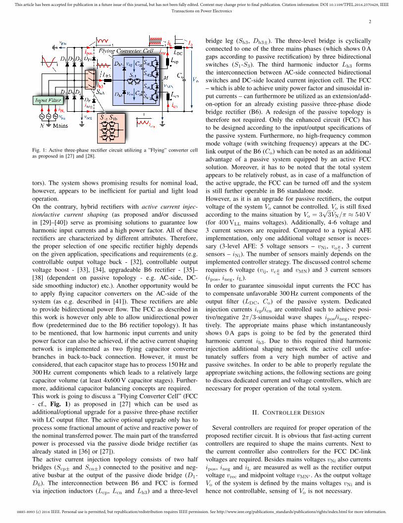
can be obtained. The required differentiator block for iLhas to be extended by a low-pass filter T1 with higher cut-off frequency for noise suppression. In Fig. 2 the derivedand advanced model in s- and z-domain (necessary due tosignal sampling) is shown which is required for proper currentcontroller design. The current controller RP/PI can be a P-typeor a PI-type controller. A convenient PI-type controller designshould also include occurring time delays (updated measuredvalue to applied duty cycle, zero order hold ZOH, etc.).All quantities are therefore transferred into the continuous q-domain (also known as w-domain) using
G# (q) = G
(z =
1 + Ts
2 q
1− Ts
2 q
)(10)
with q = jΩ and Ω = 2/Tstan(ωTs/2). The applied bilinearTustin transformation is the Pade approximation of the terme(jΩTs). The double update PWM mode of the DSP can beadvantageously be used in order to partially compensate thedelay of the uniformly sampled PWM. The sample time Ts istherefore defined by 1/ (2fs). The system should be designedsuch to achieve a rise time of ≈ 200µs which results in anΩc of 6400 rad/s with Ωmax = 0.2 · 2/Ts = 8000 rad/s.Different controllers are designed for several maximum stepresponse overshoot values of 10 %, 20 % and 40 % (as depictedin Fig. 2). The obtained quantities of R#
P/PI (q) (currentcontroller), and T#
y,i (q) (closed-loop transfer-function) haveto be transformed back into the z-plane. It can be observedthat, for a designed maximum overshoot of 40 % of the PI-type controller, actually a maximum overshoot of ≈ 50 % canbe observed. This is mainly evoked due to the additional zeroin the closed loop transfer function due to the (qTI + 1)-termof the PI-type controller and the purely integral behaviour ofGI. This effect can be compensated (or reduced) by usingeither pre-filtering technique, linear prediction KLP (z) or aSmith predictor. In order to verify proper controller design
0885-8993 (c) 2016 IEEE. Personal use is permitted, but republication/redistribution requires IEEE permission. See http://www.ieee.org/publications_standards/publications/rights/index.html for more information.
This article has been accepted for publication in a future issue of this journal, but has not been fully edited. Content may change prior to final publication. Citation information: DOI 10.1109/TPEL.2016.2570429, IEEETransactions on Power Electronics
4
Fig. 2: Advanced current controller model, including derived PI-type current controller in q-domain, poles/zeros and step response of the appropriate closedloop transfer function in the z-plane and experimental results which compare measured step response of inductance current of FCC half-bridge with derivedand calculated quantities.
and validity of the derived model, the calculated parametersare implemented in the DSP of the FCC and one half-bridgeis used as test circuit. Experimental results (cf., Fig. 2) arecompared to the calculated step response functions of Ty,i (z).As can be seen in Fig. 2 the required reference currents i∗pos [k]and i∗neg [k] are generated or originating from the passiverectifier output voltages (vpos [k] and vneg [k]) multiplied withan equivalent conductance g∗e [k]. This equivalent conductancevalue can advantageously be used to additionally charge ordischarge the FCC DC-link capacitors Ccp/Ccn. The genera-tion of g∗e and its effects on the DC-link of the FCC are goingto be discussed in the following subsection.
B. DC Voltage Control Structure
As previously discussed, the hybrid rectifier system basi-cally consists of two capacitor stages, the uncontrolled DC-linkoutput voltage Vo and the FCC DC-link voltage vcp + vcn. Inorder to reduce the number of voltage and current sensors thereference current signals for both half bridges are generatedby measuring the three mains voltages vN1−3 and the DC-sidesmoothing inductor current iL. It has to be noted that alsothe diode bridge rectifier output voltage vrec (ϕN) could bemeasured instead of vN1−3. vrec can be assessed via the mainsvoltages (vrec = max(vN1−3) − min(vN1−3)) and the trans-ferred power from the AC input to the DC output can hence
be determined by p (ϕN) = vrec (ϕN) · iL (ϕN). The evaluatedoutput power p (ϕN) is characterized by a low-frequency300 Hz ripple component. The averaged output power Po canhence be computed by using a digitally implemented low-passfilter. The dynamic of the developed (e.g. PT2) filter-type isgoing to define the step response quality of the FCC. The stepresponse of the passive rectifier LC output filter is howeveraffected according to the physical implementation of LDC andCo. The stringently required digital low-pass filter thereforehas to meet two different objectives. Firstly, the digital filterhas to be able to compete with the dynamic behaviour ofthe passive LC filter. Secondly, it has to perfectly reject the300 Hz output power ripple. In case of insufficient damping,the generated nominal currents (i∗pos, i
∗neg) and hence the
mains input currents (iNi) will show increased 6th harmonicspectral components and therefore an impaired THDi. Fig. 3depicts the voltage controller circuit with subsequent currentcontroller. If an unduly lack of FCC system dynamic isconsidered, the FCC DC voltages vcp/vcn will show a highdeviation of the expected nominal value V ∗
tot/2 for load stepsof the rectifier. This will in turn affect the proper operation ofthe DC-link voltage if vcp/vcn of one half-bridge appears tobe < VN.In order to illustrate the discussed issue more accurate, aload step of the active system is briefly discussed. In case
0885-8993 (c) 2016 IEEE. Personal use is permitted, but republication/redistribution requires IEEE permission. See http://www.ieee.org/publications_standards/publications/rights/index.html for more information.
This article has been accepted for publication in a future issue of this journal, but has not been fully edited. Content may change prior to final publication. Citation information: DOI 10.1109/TPEL.2016.2570429, IEEETransactions on Power Electronics
5
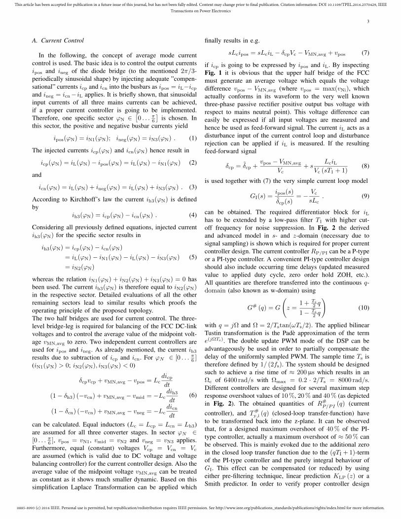
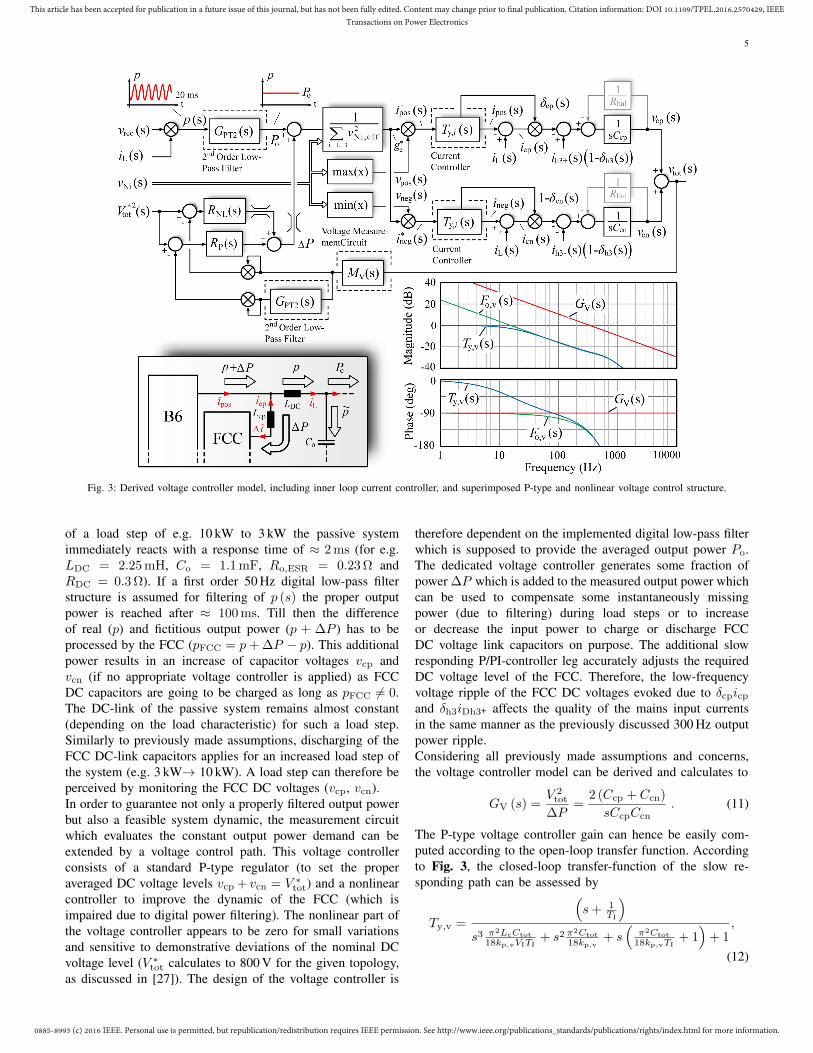
Fig. 3: Derived voltage controller model, including inner loop current controller, and superimposed P-type and nonlinear voltage control structure.
of a load step of e.g. 10 kW to 3 kW the passive systemimmediately reacts with a response time of ≈ 2 ms (for e.g.LDC = 2.25 mH, Co = 1.1 mF, Ro,ESR = 0.23 Ω andRDC = 0.3 Ω). If a first order 50 Hz digital low-pass filterstructure is assumed for filtering of p (s) the proper outputpower is reached after ≈ 100 ms. Till then the differenceof real (p) and fictitious output power (p + ∆P ) has to beprocessed by the FCC (pFCC = p+ ∆P − p). This additionalpower results in an increase of capacitor voltages vcp andvcn (if no appropriate voltage controller is applied) as FCCDC capacitors are going to be charged as long as pFCC 6= 0.The DC-link of the passive system remains almost constant(depending on the load characteristic) for such a load step.Similarly to previously made assumptions, discharging of theFCC DC-link capacitors applies for an increased load step ofthe system (e.g. 3 kW→ 10 kW). A load step can therefore beperceived by monitoring the FCC DC voltages (vcp, vcn).In order to guarantee not only a properly filtered output powerbut also a feasible system dynamic, the measurement circuitwhich evaluates the constant output power demand can beextended by a voltage control path. This voltage controllerconsists of a standard P-type regulator (to set the properaveraged DC voltage levels vcp + vcn = V ∗
tot) and a nonlinearcontroller to improve the dynamic of the FCC (which isimpaired due to digital power filtering). The nonlinear part ofthe voltage controller appears to be zero for small variationsand sensitive to demonstrative deviations of the nominal DCvoltage level (V ∗
tot calculates to 800 V for the given topology,as discussed in [27]). The design of the voltage controller is
therefore dependent on the implemented digital low-pass filterwhich is supposed to provide the averaged output power Po.The dedicated voltage controller generates some fraction ofpower ∆P which is added to the measured output power whichcan be used to compensate some instantaneously missingpower (due to filtering) during load steps or to increaseor decrease the input power to charge or discharge FCCDC voltage link capacitors on purpose. The additional slowresponding P/PI-controller leg accurately adjusts the requiredDC voltage level of the FCC. Therefore, the low-frequencyvoltage ripple of the FCC DC voltages evoked due to δcpicp
and δh3iDh3+ affects the quality of the mains input currentsin the same manner as the previously discussed 300 Hz outputpower ripple.Considering all previously made assumptions and concerns,the voltage controller model can be derived and calculates to
GV (s) =V 2
tot
∆P=
2 (Ccp + Ccn)
sCcpCcn. (11)
The P-type voltage controller gain can hence be easily com-puted according to the open-loop transfer function. Accordingto Fig. 3, the closed-loop transfer-function of the slow re-sponding path can be assessed by
Ty,v =
(s+ 1
TI
)s3 π2LcCtot
18kp,vVITI+ s2 π2Ctot
18kp,v+ s
(π2Ctot
18kp,vTI+ 1)
+ 1,
(12)
0885-8993 (c) 2016 IEEE. Personal use is permitted, but republication/redistribution requires IEEE permission. See http://www.ieee.org/publications_standards/publications/rights/index.html for more information.
This article has been accepted for publication in a future issue of this journal, but has not been fully edited. Content may change prior to final publication. Citation information: DOI 10.1109/TPEL.2016.2570429, IEEETransactions on Power Electronics
6
Fig. 4: Proposed active voltage balancing algorithm by advantageously regulat-ing the midpoint voltage v∗MN,avg = vamp · rect (ϕN) + voff implementedas rectangular signal vrect(= vamp · rect (ϕN)) with corresponding offsetvoff and appropriate DC-side smoothing inductance current iL, positive DCbus injection current icp and DC bus input current ipos.
with VI and TI as values of the designed PI-type current con-troller VI (sTI + 1) /s. Measurement results which comparecalculated and measured step-response of the system will befinally illustrated in Fig. 10 in section III. Furthermore, onlypositive power flow is allowed due to passive diode bridgerectification. The total controller minimum output is hencelimited to Pmin = Po −∆P > 0 W. The maximum limit ofthe voltage controller (Pmax) mainly depends on physicalconstraints of the B6 bridge and the FCC active switches. Theequivalent electric conductance g∗e can be determined by
g∗e =Po + ∆P∑
i=1...3
v2Ni,eff
. (13)
The reference currents of the FCC hence finally result inipos = g∗evpos, ih3 = g∗evh3 and ineg = g∗evneg . The derivedvoltage control of the active system is however merely ableto manipulate the total DC voltage level of the injection cell(vcp + vcn). In order to prevent imbalance of both voltages aDC voltage balancing concept has been derived in [42] whichis briefly discussed in the following subsection.
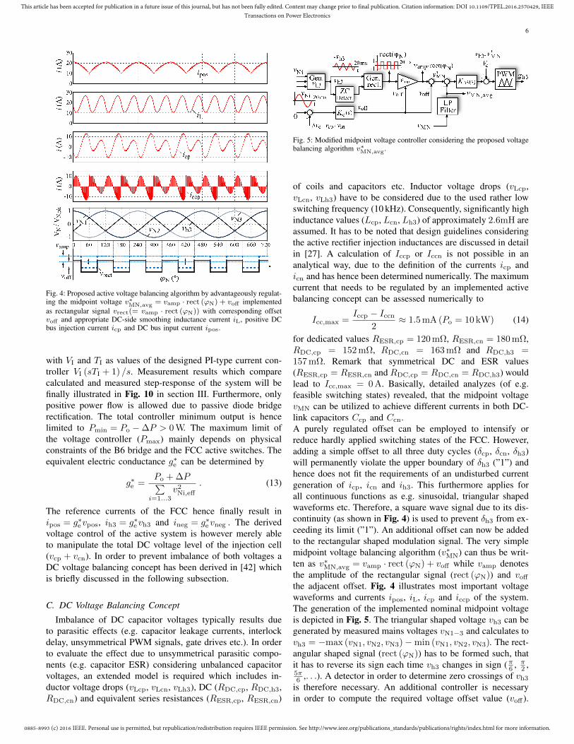
C. DC Voltage Balancing Concept
Imbalance of DC capacitor voltages typically results dueto parasitic effects (e.g. capacitor leakage currents, interlockdelay, unsymmetrical PWM signals, gate drives etc.). In orderto evaluate the effect due to unsymmetrical parasitic compo-nents (e.g. capacitor ESR) considering unbalanced capacitorvoltages, an extended model is required which includes in-ductor voltage drops (vLcp, vLcn, vLh3), DC (RDC,cp, RDC,h3,RDC,cn) and equivalent series resistances (RESR,cp, RESR,cn)
Fig. 5: Modified midpoint voltage controller considering the proposed voltagebalancing algorithm v∗MN,avg.
of coils and capacitors etc. Inductor voltage drops (vLcp,vLcn, vLh3) have to be considered due to the used rather lowswitching frequency (10 kHz). Consequently, significantly highinductance values (Lcp, Lcn, Lh3) of approximately 2.6mH areassumed. It has to be noted that design guidelines consideringthe active rectifier injection inductances are discussed in detailin [27]. A calculation of Iccp or Iccn is not possible in ananalytical way, due to the definition of the currents icp andicn and has hence been determined numerically. The maximumcurrent that needs to be regulated by an implemented activebalancing concept can be assessed numerically to
Icc,max =Iccp − Iccn
2≈ 1.5 mA (Po = 10 kW) (14)
for dedicated values RESR,cp = 120 mΩ, RESR,cn = 180 mΩ,RDC,cp = 152 mΩ, RDC,cn = 163 mΩ and RDC,h3 =157 mΩ. Remark that symmetrical DC and ESR values(RESR,cp = RESR,cn and RDC,cp = RDC,cn = RDC,h3) wouldlead to Icc,max = 0 A. Basically, detailed analyzes (of e.g.feasible switching states) revealed, that the midpoint voltagevMN can be utilized to achieve different currents in both DC-link capacitors Ccp and Ccn.A purely regulated offset can be employed to intensify orreduce hardly applied switching states of the FCC. However,adding a simple offset to all three duty cycles (δcp, δcn, δh3)will permanently violate the upper boundary of δh3 (”1”) andhence does not fit the requirements of an undisturbed currentgeneration of icp, icn and ih3. This furthermore applies forall continuous functions as e.g. sinusoidal, triangular shapedwaveforms etc. Therefore, a square wave signal due to its dis-continuity (as shown in Fig. 4) is used to prevent δh3 from ex-ceeding its limit (”1”). An additional offset can now be addedto the rectangular shaped modulation signal. The very simplemidpoint voltage balancing algorithm (v∗MN) can thus be writ-ten as v∗MN,avg = vamp · rect (ϕN) + voff while vamp denotesthe amplitude of the rectangular signal (rect (ϕN)) and voff
the adjacent offset. Fig. 4 illustrates most important voltagewaveforms and currents ipos, iL, icp and iccp of the system.The generation of the implemented nominal midpoint voltageis depicted in Fig. 5. The triangular shaped voltage vh3 can begenerated by measured mains voltages vN1−3 and calculates tovh3 = −max (vN1, vN2, vN3)−min (vN1, vN2, vN3). The rect-angular shaped signal (rect (ϕN)) has to be formed such, thatit has to reverse its sign each time vh3 changes in sign (π6 , π2 ,5π6 ,. . .). A detector in order to determine zero crossings of vh3
is therefore necessary. An additional controller is necessaryin order to compute the required voltage offset value (voff ).
0885-8993 (c) 2016 IEEE. Personal use is permitted, but republication/redistribution requires IEEE permission. See http://www.ieee.org/publications_standards/publications/rights/index.html for more information.
This article has been accepted for publication in a future issue of this journal, but has not been fully edited. Content may change prior to final publication. Citation information: DOI 10.1109/TPEL.2016.2570429, IEEETransactions on Power Electronics
7
Ideally, the calculated value has to equal the magnitude of therectangular signal (vamp = voff ) depending on the DC-linkvoltage situation (∆vc = vcp− vcn). If e.g. vcp (instantaneouscapacitor voltage of Ccp) shall be increased, a negative voltageoffset is required. This negative DC offset will simultaneouslylead to capacitor discharging of Ccn. In order to evaluatemain characteristics of the proposed balancing algorithm asimplified model of the FCC was assumed (neglecting inductorvoltage drops, parasitic components and resistances). Averagedcurrents for Ccp and Ccn can be found as
Iccp =1
6·IN · voff
(−18 + π2
√3)
πVc
Iccn = −1
6·IN · voff
(−18 + π2
√3)
πVc.
(15)
Obviously, Iccp and Iccn conform to a linear dependency ofvoff . The balancing algorithm is furthermore characterized bythe rated output power which is indicated by IN. The offsetvoff and the amplitude vamp of v∗MN,avg can hence not remainfixed for diverging loads. Assuming e.g. an offset (voff ) of 8 V(for 10 kW output power), voff has to be increased for partialand light loads to achieve similar induced capacitor currentsdue to decreased values of IN.In order to guarantee proper operation of the balancing conceptthe generated rectangular signal has to comply with a set ofconstraints which are going to be defined in the following.Considering δh3 (cf. Fig. 6(a)), vamp > 0 (1st constraint) andvamp ≥ |voff | (2nd constraint) has to be fulfilled. In order touse the maximum balancing capability, the offset voff shouldbe chosen in the same size of the rectangular amplitude vamp,voff = vamp (3rd constraint). Considering δcp,δcn positive andnegative limits for the offset voltage voff can be determined to
voff,lim = ±Vc −
√3VN
[12 + Lc
LDC
(1− 3
π
)]− ωNLcIN
2
2(16)
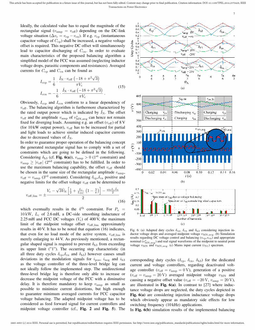
which eventually results in the 4th constraint. For Po =10 kW, Lc of 2.6 mH, a DC-side smoothing inductance of2.25 mH and FCC DC voltages (Vc) of 400 V, the maximumlimit of the midpoint voltage offset voff,lim approximatelyresults in 40 V. It has to be noted that equation (16) indicates,that even for no load mode of the active system, voff,lim ismerely enlarging to 44 V. As previously mentioned, a rectan-gular shaped signal is required to prevent δh3 from exceedingits upper limit (”1”). The occurring step characteristic (inall three duty cycles δcp,δcn and δh3) however causes smalldeviations in the modulation signals for ipos, ineg and ih3
as the voltage controller of the three-level bridge leg cannot ideally follow the implemented step. The unidirectionalthree-level bridge leg is therefore only able to increase ordecrease the midpoint voltage of the FCC with a diminutivedelay. It is therefore mandatory to keep vamp as small aspossible to minimize current distortions, but high enoughto guarantee minimum averaged currents for FCC capacitorvoltage balancing. The adapted midpoint voltage has to beconsidered as feed forward signal for current controllers andmidpoint voltage controller (cf., Fig. 2 and Fig. 5). The
(a)
(b)
(c)
Fig. 6: (a) Adapted duty cycles δcp, δcn and δh3 considering injection in-ductor voltage drops and averaged midpoint voltage vMN,avg. (b) Simulationresults regarding DC voltage control and balancing (vcp,vcn) and appropriatenominal (v∗MN,avg) and real signal waveforms of the midpoint to neutral pointvoltage vMN and vMN,avg. (c) Mains input current (iN1) spectrum.
corresponding duty cycles (δcp, δcn, δh3) for the dedicatedcurrent and voltage controllers, regarding deactivated volt-age controller (voff = vamp = 0 V), generation of a positive(voff = vamp = 20 V) averaged midpoint voltage vMN andcausing a negative offset value (voff = −20 V, vamp = 20 V),are illustrated in Fig. 6(a). In contrast to [27] where induc-tance voltage drops are neglected, the duty cycles depicted inFig. 6(a) are considering injection inductance voltage dropswhich obviously appear as mandatory side effects for lowswitching frequency (10 kHz) applications.In Fig. 6(b) simulation results of the implemented balancing
0885-8993 (c) 2016 IEEE. Personal use is permitted, but republication/redistribution requires IEEE permission. See http://www.ieee.org/publications_standards/publications/rights/index.html for more information.
This article has been accepted for publication in a future issue of this journal, but has not been fully edited. Content may change prior to final publication. Citation information: DOI 10.1109/TPEL.2016.2570429, IEEETransactions on Power Electronics
8
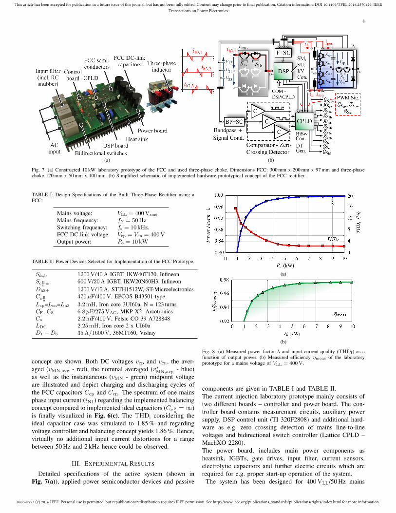
(a) (b)
Fig. 7: (a) Constructed 10 kW laboratory prototype of the FCC and used three-phase choke. Dimensions FCC: 300 mm x 200 mm x 97 mm and three-phasechoke 120 mm x 50 mm x 100 mm. (b) Simplified schematic of implemented hardware prototypical concept of the FCC rectifier.
TABLE I: Design Specifications of the Built Three-Phase Rectifier using aFCC.
TABLE II: Power Devices Selected for Implementation of the FCC Prototype.
Sia,b 1200V/40A IGBT, IKW40T120, InfineonSc p
n± 600V/20A IGBT, IKW20N60H3, Infineon
Dh3± 1200V/15A, STTH1512W, ST-MicroelectronicsCc p
n470µF/400V, EPCOS B43501-type
Lcp=Lcn=Lh3 3.2mH, Iron core 3UI60a, N = 123 turnsCF, CS 6.8µF/275VAC, MKP X2, ArcotronicsCo 2.2mF/400V, Felsic CO 39 A728848LDC 2.25mH, Iron core 2 x UI60aD1 −D6 35A/1600V, 36MT160, Vishay
concept are shown. Both DC voltages vcp and vcn, the aver-aged (vMN,avg - red), the nominal averaged (v∗MN,avg - blue)as well as the instantaneous (vMN - green) midpoint voltageare illustrated and depict charging and discharging cycles ofthe FCC capacitors Ccp and Ccn. The spectrum of one mainsphase input current (iN1) regarding the implemented balancingconcept compared to implemented ideal capacitors (Cc p
n=∞)
is finally visualized in Fig. 6(c). The THDi considering theideal capacitor case was simulated to 1.85 % and regardingvoltage controller and balancing concept yields 1.86 %. Hence,virtually no additional input current distortions for a rangebetween 50 Hz and 2 kHz hence could be observed.
III. EXPERIMENTAL RESULTS
Detailed specifications of the active system (shown inFig. 7(a)), applied power semiconductor devices and passive
(a)
(b)
Fig. 8: (a) Measured power factor λ and input current quality (THDi) as afunction of output power. (b) Measured efficiency ηmeas of the laboratoryprototype for a mains voltage of VLL = 400V.
components are given in TABLE I and TABLE II.The current injection laboratory prototype mainly consists oftwo different boards – controller and power board. The con-troller board contains measurement circuits, auxiliary powersupply, DSP control unit (TI 320F2808) and additional hard-ware as e.g. zero crossing detection of mains line-to-linevoltages and bidirectional switch controller (Lattice CPLD –MachXO 2280).The power board, includes main power components asheatsink, IGBTs, gate drives, input filter, current sensors,electrolytic capacitors and further electric circuits which arerequired for e.g. proper start-up operation of the system.
The system has been designed for 400 VLL/50 Hz mains
0885-8993 (c) 2016 IEEE. Personal use is permitted, but republication/redistribution requires IEEE permission. See http://www.ieee.org/publications_standards/publications/rights/index.html for more information.
This article has been accepted for publication in a future issue of this journal, but has not been fully edited. Content may change prior to final publication. Citation information: DOI 10.1109/TPEL.2016.2570429, IEEETransactions on Power Electronics
9
(a) (b) (c)
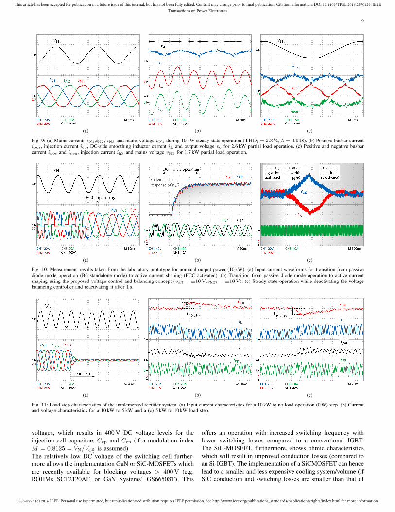
Fig. 9: (a) Mains currents iN1,iN2, iN3 and mains voltage vN1 during 10 kW steady state operation (THDi = 2.3%, λ = 0.998). (b) Positive busbar currentipos, injection current icp, DC-side smoothing inductor current iL and output voltage vo for 2.6 kW partial load operation. (c) Positive and negative busbarcurrent ipos and ineg, injection current ih3 and mains voltage vN1 for 1.7 kW partial load operation.
(a) (b) (c)
Fig. 10: Measurement results taken from the laboratory prototype for nominal output power (10 kW). (a) Input current waveforms for transition from passivediode mode operation (B6 standalone mode) to active current shaping (FCC activated). (b) Transition from passive diode mode operation to active currentshaping using the proposed voltage control and balancing concept (voff = ±10V,vMN = ±10V). (c) Steady state operation while deactivating the voltagebalancing controller and reactivating it after 1 s.
(a) (b) (c)
Fig. 11: Load step characteristics of the implemented rectifier system. (a) Input current characteristics for a 10 kW to no load operation (0 W) step. (b) Currentand voltage characteristics for a 10 kW to 5 kW and a (c) 5 kW to 10 kW load step.
voltages, which results in 400 V DC voltage levels for theinjection cell capacitors Ccp and Ccn (if a modulation indexM = 0.8125 = VN/Vc p
nis assumed).
The relatively low DC voltage of the switching cell further-more allows the implementation GaN or SiC-MOSFETs whichare recently available for blocking voltages > 400 V (e.g.ROHMs SCT2120AF, or GaN Systems’ GS66508T). This
offers an operation with increased switching frequency withlower switching losses compared to a conventional IGBT.The SiC-MOSFET, furthermore, shows ohmic characteristicswhich will result in improved conduction losses (compared toan Si-IGBT). The implementation of a SiCMOSFET can hencelead to a smaller and less expensive cooling system/volume (ifSiC conduction and switching losses are smaller than that of
0885-8993 (c) 2016 IEEE. Personal use is permitted, but republication/redistribution requires IEEE permission. See http://www.ieee.org/publications_standards/publications/rights/index.html for more information.
This article has been accepted for publication in a future issue of this journal, but has not been fully edited. Content may change prior to final publication. Citation information: DOI 10.1109/TPEL.2016.2570429, IEEETransactions on Power Electronics
10
an IGBT). The bidirectional switches can also advantageouslybe implemented by e.g. 900 V or 1200 V SiC-MOSFETs inorder to reduce losses of the current injection stage (higherexpense has to be taken into account). For proper operation,6 voltage (line-to-line voltages or vN1−3, vcp, vcn and vMN)and 3 current sensors (ipos, ineg and iL) are required. Also a5 voltage sensor solution would be possible if the third mainsphase is calculated by the already measured two remainingones. A simplified schematic of the implemented conceptof the FCC rectifier is depicted in Fig. 7(b). It is shownthat software algorithms as current/voltage controllers, start-up sequence (SU), and state machine (SM) are implementedin the digital signal processing unit. The dsp is generating theduty cycles with switching frequency for both half bridges andthe three-level bridge leg. A CPLD is furthermore required, asthe bidirectional switches have to initiate their commutation atthe same time instant when the B6 diodes are commutating. Adelay which is as small as possible is a stringent requirementin order to prevent input current distortions of the total system.The very fast updating CPLD is hence necessary which hasto evaluate the proper (100 Hz) switching sequence dependenton the mains voltage situation. Moreover, the CPLD can beused to realize the required dead time of generated PWM gatesignals gcp+ and gcn+ (of appropriate switches Scp+ and Scn+,respectively).Basic measured characteristics (efficiency ηmeas, total har-monic distortion of input currents THDi and power factor λ)of the rectifier system dependent on the provided output powerare illustrated in Fig. 8(a) and Fig. 8(b). Regarding efficiencyrates, a maximum rectifier efficiency of 97.8 % can be read atthe nominal output power of 10 kW. It has to be noted, thatthe efficiency of the passive diode rectifier for the same loadin B6 standalone operation has been obtained with 98.7 %.The assembled rectifier system furthermore achieves a THDi
below 5 % down to a output power of ≈ 3 kW. Also a powerfactor above 0.95 is measured for an output power above2.2 kW. The constructed FCC shows a good performance evenfor partial load condition (Po = 5 kW) where a THDi of2.7 % and a power factor of λ = 0.992 can be measured ata good efficiency of ηmeas = 97.5 %. As can be observed,the efficiency is decreasing for light load operation (e.g. 95 %for an output power of 1.7 kW). This effect is mainly evokeddue to the DC-side smoothing inductance current iL. Thiscurrent can be of negative value if the FCC is operating, asthe FCC is able to process both, positive and negative currentvalues. For light- and no-load condition, fractions of iL henceoccur as circulating current which has to be processed by theFCC, the DC-side smoothing inductor (LDC) and the DC-linkvoltage capacitor (Co). This circular current causes additionallosses compared to a passive standalone system during no-load operation (inductor losses LDC and Lc, switching andconduction losses etc.).The three mains currents iNi and phase voltage vN1 are shownin Fig. 9(a) for the nominal output power Po = 10 kWof the constructed laboratory prototype. The implementedPI coefficients for a switching frequency of 10 kHz, doubleupdated PWM mode and a maximum overshoot of 25 %resulted in R(z) = (0.145 − 0.1373z−1)/(1 − z−1). The
currents show (as already discussed) a THDi of 2.3 % anda power factor of λ = 0.998 can be read. Please note thatmains voltages already show a THDv of 1.7 %.Fig. 9(b) and Fig. 9(c) illustrate measurement results of mostimportant injection an regulated currents for 2.6 kW and1.7 kW, respectively. Furthermore, also the output voltage vo
of the system is depicted. It is only characterized by the typical100 Hz (according to unbalanced input voltages) and 300 Hzspectral components (very well known from the passive three-phase rectifier topology). The output voltage (which cannotbe controlled and is defined according to the mains voltagesituation) for 400 VLL input voltages has been obtained with529 V. As already discussed, Fig. 9(b) depicts the mentionednegative values of iL, which are injected by the currentsicp and icn. The appearing circulating current then resultsin a reduced system efficiency at light-load and/or no-loadcondition.Measurement results of the FCC voltages and input currentsduring the transition from B6 standalone mode to active regu-lated FCC operation are depicted in Fig. 10(a) and Fig. 10(b).The transition from passive to active diode bridge modeand the appropriate charging of the FCC DC voltage from280 V (pre-charged) to 400 V required for proper generationof injection currents for each half bridge switching leg, aretherefore illustrated. The used voltage controller gain is de-fined by kp,v=0.025 (crossover frequency 17 Hz). After theDC voltages are set to the dedicated 400 V limit they areperfectly balanced (vcp = 399.8 V, vcn = 400.1 V). Fig. 10(b)furthermore illustrates a smooth transition of both FCC DCvoltages vcp and vcn without any perceivable overshoot, whileactive voltage balancing is operating. The DC voltage balanc-ing concept is verfied in Fig. 10(c). For the proposed balancingconcept both DC voltages of the FCC are perfectly aligned.After deactivating (white area in Fig. 10(c)) the balancingalgorithm (vamp = voff = 0 V) vcp and vcn are starting todrift off the required voltage level of 400 V (Vcp = 435 V,Vcn = 365 V). Reactivating the balancing concept finallyregulate the FCC DC voltages to the expected 400 V voltagelevel.Fig. 11(a-c) illustrate different load steps for of the rectifiersystem. Fig. 11(a) depicts a full load step from nominal power(10 kW) to no-load operation of the system. As can be seen,during no-load operation there are still input currents drawn bythe system which mainly appear due to input filter capacitors(6.8µF), dedicated filter RC damping network (3 Ω, 6.8µF)and to cover system losses according to circulating currents,balancing output resistors, etc. Furthermore, the total FCC DC-link voltage vtot is illustrated in Fig. 11(b) and Fig. 11(c)for decreasing (10 kW to 5 kW) and increasing (5 kW to10 kW) load steps, respectively, while taking advantage of thepreviously discussed implemented voltage controller structure.It can be observed that the voltage deviation of the total FCCDC voltage link is defined by approximately 40 V which isabout 5 % of the defined rated voltage level V ∗
tot = V ∗cp+V ∗
cn =2 · 400 V = 800 V.
0885-8993 (c) 2016 IEEE. Personal use is permitted, but republication/redistribution requires IEEE permission. See http://www.ieee.org/publications_standards/publications/rights/index.html for more information.
This article has been accepted for publication in a future issue of this journal, but has not been fully edited. Content may change prior to final publication. Citation information: DOI 10.1109/TPEL.2016.2570429, IEEETransactions on Power Electronics
11
IV. CONCLUSION
In this work dedicated control concepts for hybrid rectifiersemploying a FCC (which basically acts as optional current in-jection unit) is discussed. The total control structure includingcurrent controller (inner loop) and voltage controller (outerloop) is presented. The proposed concept is theoretically andmathematically analyzed.Current controllers can be easily realized by a simple P/PI-type controller if vpos, vMN,avg and iL serve as feedforwardsignals.FCC DC voltage control, which can be separated into totalFCC voltage control (vcp + vcn
!= 2Vc) and FCC balancing
controller (vcp − vcn!= 0) is furthermore discussed. Emerging
issues (low-frequency distortions regarding THDi and lackof dynamic compared to a conventional passive rectificationsystem with LC output filter) due to inappropriate digital filterconcepts are addressed, which obviously require non-linearcontrol concepts for compensation. The voltage balancingconcept advantageously uses the midpoint voltage vMN of theFCC to charge or discharge the DC voltage capacitors.Both, current and voltage controller concepts have been im-plemented in a digital signal processor of a 10 kW/10 kHz lab-oratory prototype. Measurement results revealed that derivedconcepts are well suited for the proposed converter topology.
ACKNOWLEDGMENT
The authors are very much indebted to the Austrian Re-search Promotion Agency (FFG) which generously supportsthe work of the Vienna University of Technology PowerElectronics Section (Institute of Energy Systems and ElectricalDrives).
REFERENCES
[1] H.Y. Kanaan, K. Al-Haddad, and S. Rahmani, “Switch-mode powerconverters for harmonics mitigation in power systems — technologyprogress,” in IECON 2012 - 38th Annual Conference on IEEE IndustrialElectronics Society, 2012, pp. 6328–6337.
[2] J.W. Kolar and F.C Zach, “A Novel Three-Phase Three-Switch Three-Level Pwm Rectifier,” in Proceedings of the Conference for PowerElectronics, Intelligent Motion, Power Quality (PCIM), Nuernberg,Germany, June 28-30 1994, pp. 125–138.
[3] R. Bosshard and J.W. Kolar, Fundamentals and Multi-Objective De-signof Inductive Power Transfer Systems, Tutorial at the 30th AppliedPower Electronics Conference and Exposition (APEC 2015), Charlotte,NC, USA, March 15-19, 1st edition, 2005.
[4] N. Mohan, “A Novel Approach to Minimize Line-Current Harmonics inInterfacing Renewable Energy Sources with 3-Phase Utility Systems,”in Proceedings of the Seventh Annual IEEE Applied Power ElectronicsConference and Exposition (APEC), 1992, pp. 852–858.
[5] R. Naik, M. Rastogi, and N. Mohan, “Third-Harmonic Modulated PowerElectronics Interface with 3-Phase Utility to Provide a Regulated DCOutput and to Minimize Line-Current Harmonics,” in Proceedings ofthe IEEE Industry Applications Society (IAS) Annual Meeting, 1992, pp.689–694.
[6] M. Rastogi, R. Naik, and N. Mohan, “Optimization of a Novel DC-LinkCurrent Modulated Interface with 3-Phase Utility Systems to MinimizeLine Current Harmonics,” in Proceedings of the Twenty-Third AnnualIEEE Power Electronics Specialists Conference (PESC), 1992, pp. 162–167.
[7] N. Mohan, “A Novel Approach to Minimize Line-Current Harmonics inInterfacing Power Electronics Equipment with 3-Phase Utility Systems,”IEEE Transactions on Power Delivery, vol. 8, no. 3, pp. 1395–1401,1993.
[8] R. Naik, M. Rastogi, N. Mohan, R. Nilssen, and C.P. Henze, “AMagnetic Device Current Injection in a Three-Phase Sinusoidal-CurrentUtility Interface,” in Proceedings of the IEEE Industry ApplicationsSociety (IAS) Annual Meeting, 1993, pp. 926–930.
[9] S. Kim, P. Enjeti, D. Rendusara, and I.J. Pitel, “A New Method toImprove THD and Reduce Harmonics Generated by a Three-PhaseDiode Rectifier Type Utility Interface,” in Conference Record of theIEEE Industry Applications Society Annual Meeting, 1994, pp. 1071–1077.
[10] M. Rastogi, N. Mohan, and Christopher P. Henze, “Three-Phase Sinu-soidal Current Rectifier with Zero-Current Switching,” in Proceedingsof the Ninth Annual IEEE Applied Power Electronics Conference andExposition (APEC), 1994, pp. 718–724.
[11] L.R. Chaar, N. Mohan, and Christopher P. Henze, “Sinusoidal CurrentRectification in a Very Wide Range Three-Phase AC Input to a RegulatedDC Output,” in Proceedings of the Conference Record of the 1995Thirtieth IEEE Industry Applications Conference (IAS) Annual Meeting,1995, vol. 3, pp. 2341–2347.
[12] R. Naik, M. Rastogi, and N. Mohan, “Third-Harmonic ModulatedPower Electronics Interface with Three-Phase Utility to Provide aRegulated DC Output and to Minimize Line-Current Harmonics,” IEEETransactions on Industrie Applications, vol. 31, no. 3, pp. 598–602,1995.
[13] L. Chaar, G. Kamath, N. Mohan, C.P. Henze, and J.W. Kolar, “SinusoidalCurrent Rectification and Ripple Cancellation in a Very Wide ThreePhase AC Input to Generate a Regulated DC Output,” in Proceedingsof the 1996 International Conference on Power Electronics, Drives andEnergy Systems for Industrial Growth, 1996, vol. 2, pp. 644–648.
[14] Yasuyuki Nishida, “A New Simple Topology for Three-Phase Buck-Mode PFC Rectifier,” in Proceedings of the Eleventh Annual AppliedPower Electronics Conference and Exposition (APEC), 1996, vol. 2, pp.531–537.
[15] P. Pejovic and Z. Janda, “Optimal Current Programming in Three-PhaseHigh-Power-Factor Rectifier Based on Two Boost Converters,” IEEETransactions on Power Electronics, vol. 13, no. 6, pp. 1152–1163, 1998.
[16] S. Hansen, P.N. Enjeti, Jae-Hong Hahn, and F. Blaabjerg, “An IntegratedSingle-Switch Approach to Improve Harmonic Performance of StandardPWM Adjustable-Speed Drives,” IEEE Transactions on IndustrieApplications, vol. 36, no. 4, pp. 1189–1196, 2000.
[17] I. Ashida and J. Itoh, “A Novel Three-Phase PFC Rectifier Using aHarmonic Current Injection Method,” in Proceedings of the PowerConversion Conference (PCC), Nagoya, Japan, 2007, pp. 1302–1307.
[18] M. Norhisam, A. Saadon, R.N. Firdaus, I. Aris, and S.M. Bashi, “TheThree Phase Rectifier with Harmonic Injection Current,” in Proceed-ings of the IEEE Student Conference on Research and Development(SCOReD), 2010, pp. 397–400.
[19] B.M. Bird, J.F. Marsh, and P.R. McLellan, “Harmonic Reduction inMultiplex Convertors by Triple-Frequency Current Injection,” Proceed-ings of the Institution of Electrical Engineers, vol. 116, no. 10, pp.1730–1734, 1969.
[20] A. Ametani, “Generalised Method of Harmonic Reduction in AC-DC. Convertors by Harmonic Current Injection,” Proceedings of theInstitution of Electrical Engineers, vol. 119, no. 7, pp. 857–864, 1972.
[21] J.F. Baird and J. Arrilaga, “Harmonic Reduction in DC-RippleReinjection,” Proceedings of the IEE Generation, Transmission andDistribution, vol. 127, no. 5, pp. 294–303, 1980.
[22] S. Kim, P. Enjeti, P. Packebush, and I. Pitel, “A New Approach toImprove Power Factor and Reduce Harmonics in a Three Phase DiodeRectifier Type Utility Interface,” in Conference Record of the IEEEIndustry Applications Society Annual Meeting, 1993, pp. 993–1000.
[23] P. Pejovic and Z. Janda, “An Analysis of Three-Phase Low-HarmonicRectifiers Applying the Third-Harmonic Current Injection,” IEEETransactions on Power Electronics, vol. 14, no. 3, pp. 397–407, 1999.
[24] P. Pejovic and Z. Janda, “An Improved Current Injection Network forThree-Phase High-Power-Factor Rectifiers that Apply the Third Har-monic Current Injection,” IEEE Transactions on Industrial Electronics,vol. 47, no. 2, pp. 497–499, 2000.
[25] P. Pejovic, “A Novel Low-Harmonic Three-Phase Rectifier,” IEEETransactions on Circuits and Systems, vol. 49, no. 7, pp. 955–965, 2002.
[26] P. Pejovic, P. Bozovic, and I. Pavlovic, “A Novel Magnetic Device forCurrent Injection Based Three-Phase Low-Harmonic Rectifiers that Inte-grates the Current Injection Device and the Inductor,” in Proceedings ofthe third IET International Conference on Power Electronics, Machinesand Drives, 2006, pp. 80–84.
[27] M. Hartmann and R. Fehringer, “Active Three-Phase Rectifier SystemUsing a “Flying” Converter Cell,” in Proceedings of the InternationalEnergy Conference and Exhibition (ENERGYCON), 2012, pp. 82–89.
0885-8993 (c) 2016 IEEE. Personal use is permitted, but republication/redistribution requires IEEE permission. See http://www.ieee.org/publications_standards/publications/rights/index.html for more information.
This article has been accepted for publication in a future issue of this journal, but has not been fully edited. Content may change prior to final publication. Citation information: DOI 10.1109/TPEL.2016.2570429, IEEETransactions on Power Electronics
12
[28] M. Hartmann, R. Fehringer, M. Makoschitz, and H. Ertl, “Design andExperimental Verification of a Third Harmonic Injection Rectifier CircuitUsing a Flying Converter Cell,” in Proceedings of the Twenty-NinthAnnual IEEE Applied Power Electronics Conference and Exposition(APEC), 2014, pp. 920–927.
[29] J.C. Salmon, “Operating a Three-Phase Diode Rectifier with a Low-Input Current Distortion Using a Series-Connected Dual Boost Con-verter,” IEEE Transactions on Power Electronics, vol. 11, no. 4, pp.592–603, 1996.
[30] J. Salmon, E. Nowicki, Wilsun Xu, and D. Koval, “Low Distortion 3-Phase Rectifiers Utilizing Harmonic Correction Circuit Topologies withBoth IGBT and Thyristor Switches,” in Proceedings of the ThirteenthAnnual IEEE Applied Power Electronics Conference and Exposition(APEC), 1998, vol. 2, pp. 1100–1106.
[31] T.B. Soeiro, T. Friedli, and J.W. Kolar, “Swiss Rectifier — A NovelThree-Phase Buck-Type PFC Topology for Electric Vehicle BatteryCharging,” in Proceedings of the Twenty-Seventh Annual IEEE AppliedPower Electronics Conference and Exposition (APEC), 2012, pp. 2617–2624.
[32] T. B. Soeiro, T. Friedli, and J. W. Kolar, “Design and Implementationof a Three-Phase Buck-Type Third Harmonic Current Injection PFCRectifier SR,” IEEE Transactions on Power Electronics, vol. 28, no. 4,pp. 1608–1621, 2013.
[33] H.Y. Kanaan and K. Al-Haddad, “Three-Phase Current-Injection Rec-tifiers: Competitive Topologies for Power Factor Correction,” IEEEIndustrial Electronics Magazine, vol. 6, no. 3, pp. 24–40, 2012.
[34] H. Y. Kanaan, H. Fortin-Blanchette, K. Al-Haddad, R. Chaffai,L. Duguay, and F. Fnaiech, “Linear Control Design for a Current-Injection-Based Three-Phase Unity-Power-Factor Rectifier,” IEEETransactions on Industrial Electronics, vol. 51, no. 2, pp. 429–438, Apr.2004.
[35] X. Du, L. Zhou, H. Lu, and H.-M. Tai, “DC Link Active PowerFilter for Three-Phase Diode Rectifier,” IEEE Transactions on IndustrialElectronics, vol. 59, no. 3, pp. 1430–1442, 2012.
[36] N. Vazquez, H. Rodriguez, C. Hernandez, E. Rodriguez, and J. Arau,“Three-Phase Rectifier With Active Current Injection and High Effi-ciency,” IEEE Transactions on Industrial Electronics, vol. 56, no. 1, pp.110–119, 2009.
[37] H. Yoo and Seung-Ki Sul, “A New Circuit Design and Control toReduce Input Harmonic Current for a Three-Phase AC Machine DriveSystem Having a Very Small DC-Link Capacitor,” in in Proceedingsof the Twenty-Fifth Annual IEEE Applied Power Electronics Conferenceand Exposition (APEC), 2010, pp. 611–618.
[38] M. Makoschitz, M. Hartmann, and H. Ertl, “Topology Survey ofDC-Side Enhanced Passive Rectifier Circuits for Low-Harmonic InputCurrents and Improved Power Factor,” in Proceedings of InternationalExhibition and Conference for Power Electronics, Intelligent Motion,Renewable Energy and Energy Management (PCIM Europe), May 2015,pp. 1–8.
[39] H. Yoo and Seung-Ki Sul, “A Novel Approach to Reduce Line HarmonicCurrent for a Three-phase Diode Rectifier-Fed Electrolytic CapacitorlessInverter,” in Proceedings of the Twenty-Fourth Annual IEEE AppliedPower Electronics Conference and Exposition (APEC), 2009, pp. 1897–1903.
[40] R.A. Rached, H.Y. Kanaan, and K. Al-Haddad, “Three-Phase Rectifierwith an Active Current Injection and a Single High-Frequency Inductor,”in Proceedings of the Energy Conversion Congress and Exposition(ECCE), 2010, pp. 2074–2078.
[41] Bhim Singh, B.N. Singh, A. Chandra, K. Al-Haddad, A. Pandey, and
D.P. Kothari, “A Review of Three-Phase Improved Power Quality AC-DC Converters,” IEEE Transactions on Industrial Electronics, vol. 51,no. 3, pp. 641–660, 2004.
[42] M. Makoschitz, M. Hartmann, H. Ertl, and R. Fehringer, “DC VoltageBalancing of Flying Converter Cell,” in Proceedings of the EnergyConversion Congress and Exposition (ECCE), 2014, pp. 4071–4078.
Markus Makoschitz (S’14) was born in ViennaAustria, on May 22, 1987. He received the B.Sc.and M.Sc. degrees (Hons.) in electrical engineeringfrom the Vienna University of Technology, in 2010and 2012, respectively. He is currently workingtowards his Ph.D degree at the Vienna Universityof Technology, where he is engaged in research onactive three-phase PFC rectifier systems.
Michael Hartmann (M’11) received the B.S. degree(Hons.) and the M.Sc. degree (Hons.) in electri-cal engineering from the University of Technol-ogy Vienna, Vienna, Austria, in 2005 and 2006,respectively. In summer 2011, he received the Ph.D.degree from the Power Electronic Systems Labora-tory, Swiss Federal Institute of Technology, Zurich,Switzerland, where his research was focused onactive three-phase rectifier systems with ultrahighswitching frequencies and three-phase rectifiers foraircraft applications. He is currently with Schneider
Electric, Drive Technology and Systems in Vienna, where he is involvedin the research on high efficiency three-phase power converter systems forlow and medium voltage power drives. His research interests further includethree-phase power conversion, electromagnetic interference and switched-mode power amplifiers using multicell topologies.
Dr. Hartmann received the IEEE PELS Prize Paper Award in 2012.
Hans Ertl (M’93) received the Dipl.-Ing. (M.Sc.)degree and the Ph.D. degree in industrial electronicsfrom the University of Technology Vienna, Vienna,Austria, in 1984 and 1991, respectively. Since 1984,he has been with the Vienna University of Technol-ogy, where he is currently an Associate Professorwith the Power Electronics Section of the Instituteof Electrical Drives and Machines. He has performednumerous industrial and scientific research projectsin the areas of field-oriented control of ac drivesystems, switch-mode power supplies for welding
and industrial plasma processes, and active rectifier systems. He is theauthor or coauthor of numerous scientific papers and patents. His currentresearch activities are focused on switch-mode power amplifiers and multicelltopologies, in particular, for the generation of testing signals, for active ripplecurrent compensators, and for several applications in the area of renewableenergy systems.


![Ppt b6 [recuperado]](https://static.documents.pub/doc/80x56/559e6d381a28abba458b4799/ppt-b6-recuperado.jpg)


