Cool-Power ® ZVS Switching Regulators Rev 1.2 Page 1 of 17 02/2017 11V IN to 36V IN , 5V OUT , 15A, Cool-Power ZVS Buck Regulator Cool-Power ® ZVS Switching Regulators PI3302-03 Product Description The PI3302-03 is a high efficiency, wide input range DC-DC ZVS Buck Regulator integrating controller, power switches, and support components all within a high density System-in-Package (SiP). The integration of a high performance Zero-Voltage Switching (ZVS) topology, within the PI3302-03 model, increases point of load performance providing best in class power efficiency. The PI3302-03 requires only an external inductor and minimal capacitors to form a complete DC-DC switching mode Buck Regulator. The ZVS architecture also enables high frequency operation while minimizing switching losses and maximizing efficiency. The high switching frequency operation reduces the size of the external filtering components, improves power density, and enables very fast dynamic response to line and load transients. Features & Benefits • High Efficiency ZVS-Buck Topology • Wide input voltage range of 11V to 36V • Output power up to 75W • Very fast transient response • High accuracy pre-trimmed output voltage • User adjustable soft-start & tracking • Parallel capable with single wire current sharing • Input Over/Undevoltage Lockout (OVLO/UVLO) • Output Overvoltage Protection (OVP) • Overtemperature Protection (OTP) • Fast and slow current limits • -40°C to 125°C operating range (T J ) Applications • High efficiency systems • Computing, Communications, Industrial, Automotive Equipment • High voltage battery operation Package Information • 10mm x 14mm x 2.6mm (LGA SiP) Device Output Voltage I OUT Max Set Range PI3302-03-LGIZ 5.0V 3.3 to 6.5V 15A * I 2 C™ is a trademark of NXP Semiconductors
Transcript
Cool-Power® ZVS Switching Regulators Rev 1.2Page 1 of 17 02/2017
11VIN to 36VIN, 5VOUT, 15A, Cool-Power ZVS Buck Regulator
Cool-Power®
ZVS Switching RegulatorsPI3302-03
Product Description
The PI3302-03 is a high efficiency, wide input range DC-DC ZVS Buck Regulator integrating controller, power switches, and support components all within a high density System-in-Package (SiP). The integration of a high performance Zero-Voltage Switching (ZVS) topology, within the PI3302-03 model, increases point of load performance providing best in class power efficiency. The PI3302-03 requires only an external inductor and minimal capacitors to form a complete DC-DC switching mode Buck Regulator.
The ZVS architecture also enables high frequency operation while minimizing switching losses and maximizing efficiency. The high switching frequency operation reduces the size of the external filtering components, improves power density, and enables very fast dynamic response to line and load transients.
Features & Benefits
• High Efficiency ZVS-Buck Topology
• Wide input voltage range of 11V to 36V
• Output power up to 75W
• Very fast transient response
• High accuracy pre-trimmed output voltage
• User adjustable soft-start & tracking
• Parallel capable with single wire current sharing
Cool-Power® ZVS Switching Regulators Rev 1.2Page 2 of 17 02/2017
PI3302-03
Contents
Order Information 3
Absolute Maximum Ratings 3
Functional Block Diagram 3
Pin Description 4
Package Pin-Out 4
Electrical Characteristics 5
PI3302-03 (5.0VOUT) Electrical Characteristics 7
Functional Description 9
ENABLE (EN) 9
Remote Sensing 9
Switching Frequency Synchronization 9
Soft-Start 9
Output Voltage Trim 9
Output Current Limit Protection 9
Input Undervoltage Lockout 9
Input Overvoltage Lockout 9
Output Overvoltage Protection 10
Overtemperature Protection 10
Pulse Skip Mode (PSM) 10
Variable Frequency Operation 10
Parallel Operation 10
Application Description 10
Output Voltage Trim 10
Soft-Start Adjust and Tracking 11
Inductor Pairing 11
Thermal Derating 12
I2C™ Operation 12
Filter Considerations 12
Layout Guidelines 13
Recommended PCB Footprint and Stencil 14
LGIZ Package Drawing 15
Revision History 16
Product Warranty 17
Cool-Power® ZVS Switching Regulators Rev 1.2Page 3 of 17 02/2017
PI3302-03
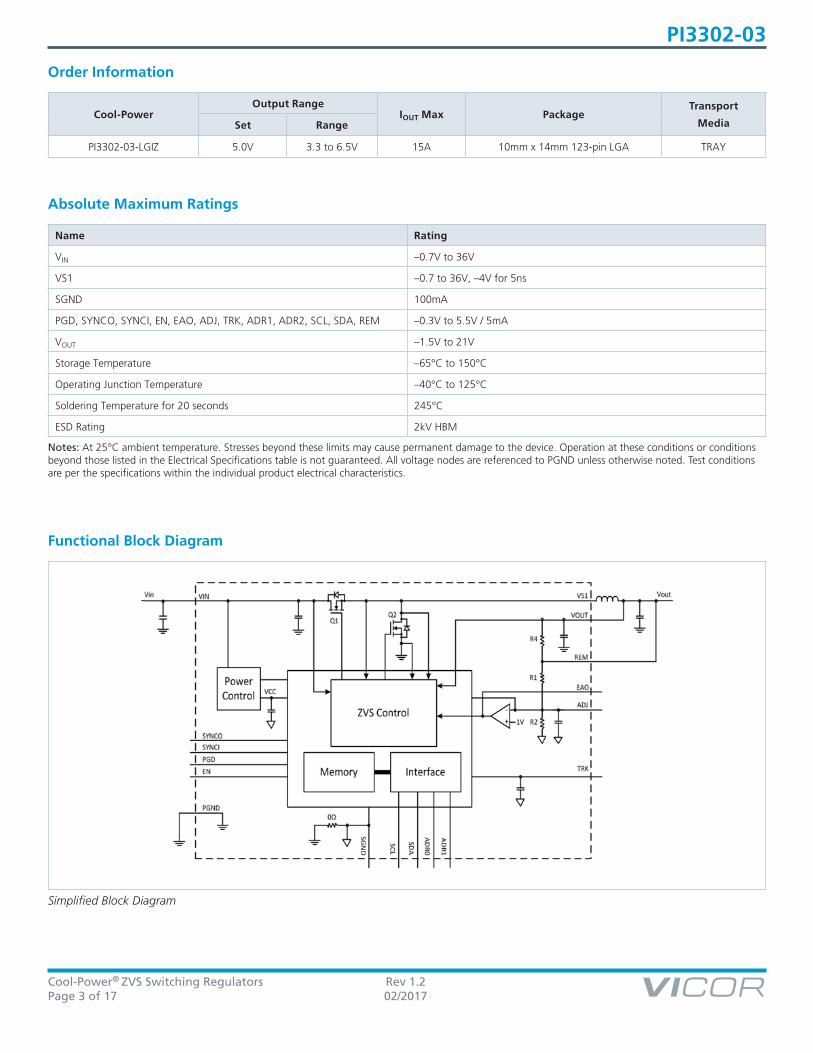
Order Information
Notes: At 25°C ambient temperature. Stresses beyond these limits may cause permanent damage to the device. Operation at these conditions or conditions beyond those listed in the Electrical Specifications table is not guaranteed. All voltage nodes are referenced to PGND unless otherwise noted. Test conditions are per the specifications within the individual product electrical characteristics.
Cool-PowerOutput Range
IOUT Max PackageTransport
MediaSet Range
PI3302-03-LGIZ 5.0V 3.3 to 6.5V 15A 10mm x 14mm 123-pin LGA TRAY
Name Rating
VIN –0.7V to 36V
VS1 –0.7 to 36V, –4V for 5ns
SGND 100mA
PGD, SYNCO, SYNCI, EN, EAO, ADJ, TRK, ADR1, ADR2, SCL, SDA, REM –0.3V to 5.5V / 5mA
VOUT –1.5V to 21V
Storage Temperature –65°C to 150°C
Operating Junction Temperature –40°C to 125°C
Soldering Temperature for 20 seconds 245°C
ESD Rating 2kV HBM
Absolute Maximum Ratings
Functional Block Diagram
Simplified Block Diagram
Cool-Power® ZVS Switching Regulators Rev 1.2Page 4 of 17 02/2017
PI3302-03
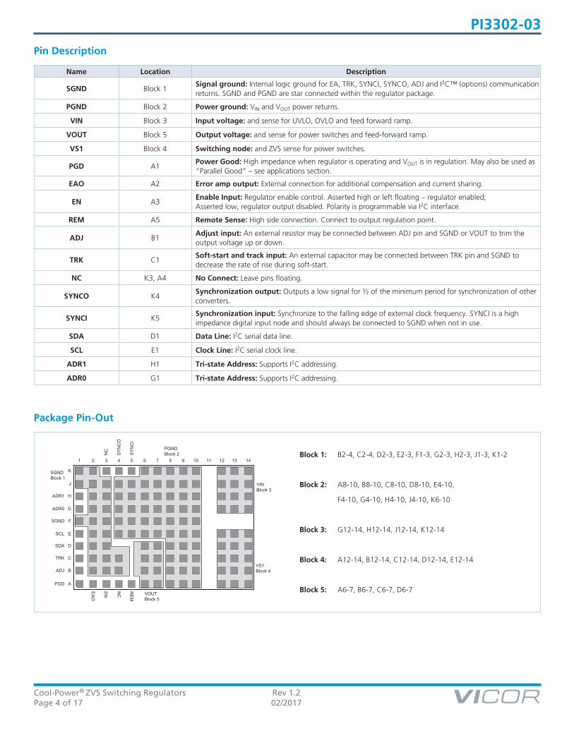
Pin Description
Name Location Description
SGND Block 1Signal ground: Internal logic ground for EA, TRK, SYNCI, SYNCO, ADJ and I2C™ (options) communication returns. SGND and PGND are star connected within the regulator package.
PGND Block 2 Power ground: VIN and VOUT power returns.
VIN Block 3 Input voltage: and sense for UVLO, OVLO and feed forward ramp.
VOUT Block 5 Output voltage: and sense for power switches and feed-forward ramp.
VS1 Block 4 Switching node: and ZVS sense for power switches.
PGD A1Power Good: High impedance when regulator is operating and VOUT is in regulation. May also be used as “Parallel Good” – see applications section.
EAO A2 Error amp output: External connection for additional compensation and current sharing.
EN A3Enable Input: Regulator enable control. Asserted high or left floating – regulator enabled; Asserted low, regulator output disabled. Polarity is programmable via I2C interface.
REM A5 Remote Sense: High side connection. Connect to output regulation point.
ADJ B1Adjust input: An external resistor may be connected between ADJ pin and SGND or VOUT to trim the output voltage up or down.
TRK C1Soft-start and track input: An external capacitor may be connected between TRK pin and SGND to decrease the rate of rise during soft-start.
NC K3, A4 No Connect: Leave pins floating.
SYNCO K4Synchronization output: Outputs a low signal for ½ of the minimum period for synchronization of other converters.
SYNCI K5Synchronization input: Synchronize to the falling edge of external clock frequency. SYNCI is a high impedance digital input node and should always be connected to SGND when not in use.
Overtemperature Fault Threshold TOTP[2] 130 135 140 °C
Overtemperature Restart Hysteresis TOTP_HYS 30 °C
Timing
Switching Frequency fS[6] 0.800 MHz
Fault Restart Delay tFR_DLY 36 ms
Sync In (SYNCI)
Synchronization Frequency Range ∆fSYNCI Relative to set switching frequency [3] 50 110 %
SYNCI Threshold VSYNCI 2.5 V
Cool-Power® ZVS Switching Regulators Rev 1.2Page 6 of 17 02/2017
PI3302-03
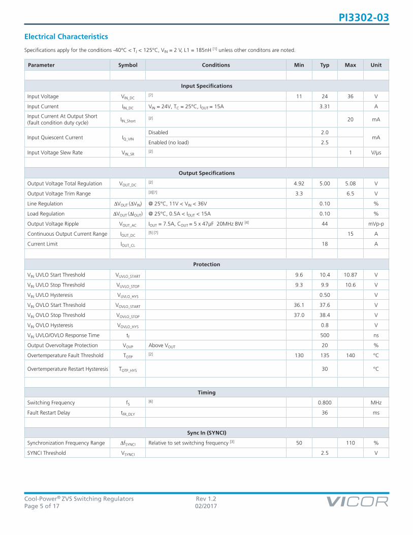
[1] All parameters reflect regulator and inductor system performance. Measurements were made using a standard PI3302-03 evaluation board with 3x4” dimensions and 4 layer, 2oz copper. Refer to inductor pairing table within Application Description section for specific inductor manufacturer and value.
[2] Regulator is assured to meet performance specifications by design, test correlation, characterization, and/or statistical process control.[3] Output current capability may be limited and other performance may vary from electrical characteristics when switching frequency or VOUT is modified.[4] Refer to Output Ripple plots.[5] Refer to Load Current vs. Ambient Temperature curves.[6] Refer to Switching Frequency vs. Load current curves.[7] VIN – VOUT must be 5V or more to avoid a minimum load requirement of 3mA. Regulator must be disabled if VIN – VOUT is less than 1V.
Electrical Characteristics (Cont.)
Specifications apply for the conditions -40°C < TJ < 125°C, VIN = 24V, L1 = 185nH [1] unless other conditons are noted.
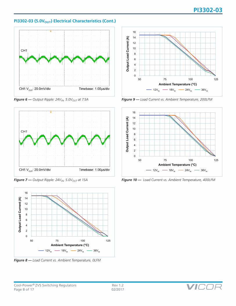
Figure 8 — Load Current vs. Ambient Temperature, 0LFM
Ambient Temperature (°C)
Out
put L
oad
Cur
rent
(A)
12VIN 18VIN 24VIN 36VIN
0
2
4
6
8
10
12
14
16
50 75 100 125
Figure 10 — Load Current vs. Ambient Temperature, 400LFM
Cool-Power® ZVS Switching Regulators Rev 1.2Page 9 of 17 02/2017
PI3302-03
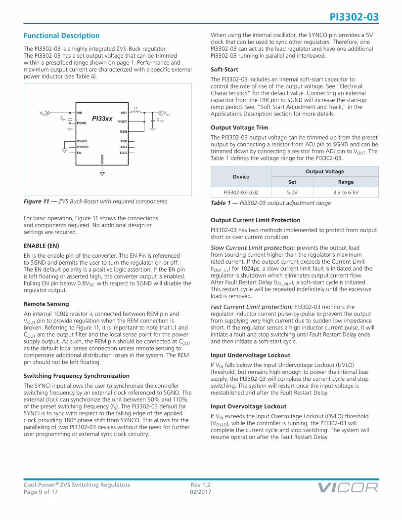
Functional Description
The PI3302-03 is a highly integrated ZVS-Buck regulator. The PI3302-03 has a set output voltage that can be trimmed within a prescribed range shown on page 1. Performance and maximum output current are characterized with a specific external power inductor (see Table 4).
For basic operation, Figure 11 shows the connections and components required. No additional design or settings are required.
ENABLE (EN)
EN is the enable pin of the converter. The EN Pin is referenced to SGND and permits the user to turn the regulator on or off. The EN default polarity is a positive logic assertion. If the EN pin is left floating or asserted high, the converter output is enabled. Pulling EN pin below 0.8VDC with respect to SGND will disable the regulator output.
Remote Sensing
An internal 100Ω resistor is connected between REM pin and VOUT pin to provide regulation when the REM connection is broken. Referring to Figure 11, it is important to note that L1 and COUT are the output filter and the local sense point for the power supply output. As such, the REM pin should be connected at COUT as the default local sense connection unless remote sensing to compensate additional distribution losses in the system. The REM pin should not be left floating.
Switching Frequency Synchronization
The SYNCI input allows the user to synchronize the controller switching frequency by an external clock referenced to SGND. The external clock can synchronize the unit between 50% and 110% of the preset switching frequency (fS). The PI3302-03 default for SYNCI is to sync with respect to the falling edge of the applied clock providing 180° phase shift from SYNCO. This allows for the paralleling of two PI3302-03 devices without the need for further user programming or external sync clock circuitry.
When using the internal oscillator, the SYNCO pin provides a 5V clock that can be used to sync other regulators. Therefore, one PI3302-03 can act as the lead regulator and have one additional PI3302-03 running in parallel and interleaved.
Soft-Start
The PI3302-03 includes an internal soft-start capacitor to control the rate of rise of the output voltage. See “Electrical Characteristics” for the default value. Connecting an external capacitor from the TRK pin to SGND will increase the start-up ramp period. See, “Soft Start Adjustment and Track,” in the Applications Description section for more details.
Output Voltage Trim
The PI3302-03 output voltage can be trimmed up from the preset output by connecting a resistor from ADJ pin to SGND and can be trimmed down by connecting a resistor from ADJ pin to VOUT. The Table 1 defines the voltage range for the PI3302-03.
Output Current Limit Protection
PI3302-03 has two methods implemented to protect from output short or over current condition.
Slow Current Limit protection: prevents the output load from sourcing current higher than the regulator’s maximum rated current. If the output current exceeds the Current Limit (IOUT_CL) for 1024µs, a slow current limit fault is initiated and the regulator is shutdown which eliminates output current flow. After Fault Restart Delay (tFR_DLY), a soft-start cycle is initiated. This restart cycle will be repeated indefinitely until the excessive load is removed.
Fast Current Limit protection: PI3302-03 monitors the regulator inductor current pulse-by-pulse to prevent the output from supplying very high current due to sudden low impedance short. If the regulator senses a high inductor current pulse, it will initiate a fault and stop switching until Fault Restart Delay ends and then initiate a soft-start cycle.
Input Undervoltage Lockout
If VIN falls below the input Undervoltage Lockout (UVLO) threshold, but remains high enough to power the internal bias supply, the PI3302-03 will complete the current cycle and stop switching. The system will restart once the input voltage is reestablished and after the Fault Restart Delay.
Input Overvoltage Lockout
If VIN exceeds the input Overvoltage Lockout (OVLO) threshold (VOVLO), while the controller is running, the PI3302-03 will complete the current cycle and stop switching. The system will resume operation after the Fault Restart Delay.
EN SGN
D
VIN VIN
VOUT
SYNCI
VS1 VOUT
PGND
SYNCO
REM
TRK
ADJ
EAO
PI33xxCIN COUT
L1
Figure 11 — ZVS Buck-Boost with required components
DeviceOutput Voltage
Set Range
PI3302-03-LGIZ 5.0V 3.3 to 6.5V
Table 1 — PI3302-03 output adjustment range
Cool-Power® ZVS Switching Regulators Rev 1.2Page 10 of 17 02/2017
PI3302-03
Output Overvoltage Protection
The PI3302-03 is equipped with output Overvoltage Protection (OVP) to prevent damage to input voltage sensitive devices. If the output voltage exceeds 20% of its set regulated value, the regulator will complete the current cycle, stop switching and issue an OVP fault. The system will resume operation once the output voltage falls below the OVP threshold and after Fault Restart Delay.
Overtemperature Protection
The internal package temperature is monitored to prevent internal components from reaching their thermal maximum. If the Overtemperature Protection Threshold (OTP) is exceeded (TOTP), the regulator will complete the current switching cycle, enter a low power mode, set a fault flag, and will soft-start when the internal temperature falls below Overtemperature Restart Hysteresis (TOTP_HYS).
Pulse Skip Mode (PSM)
PI3302-03 features a PSM to achieve high efficiency at light loads. The regulators are setup to skip pulses if EAO falls below a PSM threshold. Depending on conditions and component values, this may result in single pulses or several consecutive pulses followed by skipped pulses. Skipping cycles significantly reduces gate drive power and improves light load efficiency. The regulator will leave PSM once the EAO rises above the Skip Mode threshold.
Variable Frequency Operation
Each PI3302-03 is preprogrammed to a base operating frequency, with respect to the power stage inductor (see Table 3), to operate at peak efficiency across line and load variations. At low line and high load applications, the base frequency will decrease to accommodate these extreme operating ranges. By stretching the frequency, the ZVS operation is preserved throughout the total input line voltage range therefore maintaining optimum efficiency.
Parallel Operation
Paralleling modules can be used to increase the output current capability of a single power rail and reduce output voltage ripple.
The PI3302-03 default for SYNCI is to sync with respect to the falling edge of the applied clock providing 180° phase shift from SYNCO. This allows for the paralleling of two PI3302-03 devices without the need for further user programming or external sync clock circuitry.
By connecting the EAO pins and SGND pins of each module together the units will share the current equally. When the TRK pins of each unit are connected together, the units will track each other during soft-start and all unit EN pins have to be released to allow the units to start (See Figure 12). Also, any fault event in any regulator will disable the other regulators. The two regulators will be out of phase with each other reducing output ripple (refer to Switching Frequency Synchronization).
To provide synchronization between regulators over the entire operational frequency range, the Power Good (PGD) pin must be connected to the lead regulator’s (#1) SYNCI pin and a 2.5kΩ Resistor, R1, must be placed between SYNCO (#2) return and the lead regulator’s SYNCI (#1) pin, as shown in Figure 12. In this configuration, at system soft-start, the PGD pin pulls SYNCI low forcing the lead regulator to initialize the open-loop startup synchronization. Once the regulators reach regulation, SYNCI is released and the system is now synchronized in a closed-loop configuration which allows the system to adjust, on the fly, when any of the individual regulators begin to enter variable frequency mode in the loop.
Application Description
Output Voltage Trim
With a single resistor connected from the ADJ pin to SGND or REM, a device’s output can be varied above or below the nominal set voltage. The remote pin (REM) should always be connected to the VOUT pin, if not used, to prevent an output voltage offset. Figure 13 shows the internal feedback voltage divider network.
SGND
VS1
PGND
REM
TRK
EAO
(#1)
SGND
VS1
PGND
REM(#2)
EN
EAO(#2)
TRK(#2)
EN(#2)
PGDSYNCI
SYNCOSYNCI(#2)
SYNCO(#2)R1
TRK
EAO
EN
EAO(#1)TRK(#1)
EN(#1)
PGDSYNCI
SYNCOSYNCI(#1)
SYNCO(#1)
VIN VIN
VOUT
VIN
VOUT
VOUT
CIN COUT
L1
L1VIN
CIN COUT
PI33xx
PI33xx
Figure 12 — PI3302-03 parallel operation
+- ADJ
REM
VOUT
R2
R1
R4
SGND
Rlow
Rhigh1.0VDC
Figure 13 — Internal resistor divider network
Cool-Power® ZVS Switching Regulators Rev 1.2Page 11 of 17 02/2017
PI3302-03
R1, R2, and R4 are all internal 1.0% resistors and Rlow and Rhigh are external resistors which the designer can add to modify VOUT to a desired output. The internal resistor value for each regulator is listed below in Table 2.
By choosing an output voltage value within the ranges stated in Table 1, VOUT can simply be adjusted up or down by selecting the proper Rhigh or Rlow value, respectively. The following equations can be used to calculate Rhigh an Rlow values:
Soft-Start Adjust and Tracking
The TRK pin offers a means to increase the regulator’s soft-start time or to track with additional regulators. The soft-start slope is controlled by an internal capacitor and a fixed charge current to provide a Soft-Start Time tSS for all PI3302-03 regulators. By adding an additional external capacitor to the TRK pin, the soft-start time can beincreased further. The following equation can be used to calculate the proper capacitor for a desired soft-start times:
Where, tTRK is the soft-start time and ITRK is a 50µA internal charge current (see Electrical Characteristics for limits).
There is typically either proportional or direct tracking implemented within a design. For proportional tracking between several regulators at startup, simply connect all PI3302-03 device TRK pins together. This type of tracking will force all connected regulators to startup and reach regulation at the same time (see Figure 14).
For Direct Tracking, choose the PI3302-03 or power supply with the highest output voltage as the master and connect the master output voltage to the TRK pin of the other PI3302-03 regulator(s) through a divider (Figure 15) with the same ratio as the slave’s feedback divider (see Table 2 for values).
All connected PI3302-03 regulator soft-start slopes will track with this method. Direct tracking timing is demonstrated in Figure 14b. All tracking regulators should have their Enable (EN) pins connected together to work properly.
Inductor Pairing
The PI3302-03 utilizes an external inductor. This inductor has been optimized for maximum efficiency performance. Table 3 details the specific inductor value and part number utilized for the PI3302-03 device and is available from Eaton Corp.
Conditions R1 R2 R4
PI3302-03-LGIZ 4.53kΩ 1.13kΩ 100Ω
Table 2 — PI3302-03 Internal divider values
1Rhigh
R1( )VOUT – 1 1
R2–=
( )(1)
CTRK = (3)tTRK • ITRK – 100 • 10 -9( )
1Rlow
R2( )VOUT – 11
R1–
= ( )1(2)
VOUT 1
VOUT 2
Master VOUT
VOUT 2
(a)
(b)+
Figure 14 — PI3302-03 tracking methods
Master VOUT
R1
R2
SGND
TRK
PI33xx
Slave
Figure 15 — Voltage divider connections for direct tracking
DeviceInductor
(nH)Inductor
Part NumberManufacturer
PI3302-03 185 FP1507R1-R185-R Eaton Corp.
Table 3 — PI3302-03 Inductor pairing
Cool-Power® ZVS Switching Regulators Rev 1.2Page 12 of 17 02/2017
PI3302-03
Thermal Derating
Thermal de-rating curves are provided that are based on component temperature changes versus load current, input voltage and air flow. It is recommended to use these curves as a guideline for proper thermal de-rating. These curves represent the entire system and are inclusive to both the Vicor regulator and the external inductor. Maximum thermal operation is limited by either the MOSFETs or inductor depending upon line and load conditions.
Thermal measurements were made using a standard PI3302-03 Evaluation board which is 3x4 inches in area and uses 4-layer, 2oz copper. Thermal measurements were made on the three main power devices, the two internal MOSFETs and the external inductor, with air flows of 0, 200, and 400LFM.
I2C™ Operation
The PI3302-03 provides an I2C digital interface that enables the user to program EN pin polarity, frequency synchronization phase/delay, dynamic margining and fault monitoring. The fault telemetry that can be monitored is:
nn Input under and overvoltage (UV/OV)
nn Output voltage too high
nn Fast and slow current limit
nn Overtemperature protection
Please refer to PI33XX-2X I2C Digital Interface Guide for details.
Filter Considerations
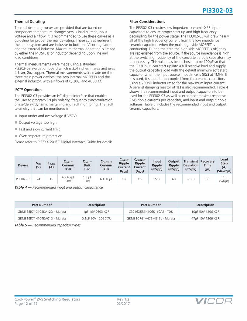
The PI3302-03 requires low impedance ceramic X5R input capacitors to ensure proper start up and high frequency decoupling for the power stage. The PI3302-03 will draw nearly all of the high frequency current from the low impedance ceramic capacitors when the main high side MOSFET is conducting. During the time the high side MOSFET is off, they are replenished from the source. If the source impedance is high at the switching frequency of the converter, a bulk capacitor may be necessary. This value has been chosen to be 100µF so that the PI3302-03 can start up into a full resistive load and supply the output capacitive load with the default minimum soft start capacitor when the input source impedance is 50Ω at 1MHz. If it is used, it should be decoupled from the ceramic capacitors using a 200nH inductor rated for the maximum input current. A parallel damping resistor of 1Ω is also recommended. Table 4 shows the recommended input and output capacitors to be used for the PI3302-03 as well as expected transient response, RMS ripple currents per capacitor, and input and output ripple voltages. Table 5 includes the recommended input and output ceramic capacitors.
Table 4 — Recommended input and output capacitance
Cool-Power® ZVS Switching Regulators Rev 1.2Page 13 of 17 02/2017
PI3302-03
Layout Guidelines
To optimize maximum efficiency and low noise performance from a PI3302-03 design, layout considerations are necessary. Reducing trace resistance and minimizing high current loop returns along with proper component placement will contribute to optimized performance.
A typical buck converter circuit is shown in Figure 16. The potential areas of high parasitic inductance and resistance are the circuit return paths, shown as LR below.
The path between the COUT and CIN capacitors is of particular importance since the AC currents are flowing through both of them when Q1 is turned on. Figure 17, schematically, shows the reduced trace length between input and output capacitors. The shorter path lessens the effects that copper trace parasitics can have on the PI3302-03 performance.
When Q1 is on and Q2 is off, the majority of CIN’s current is used to satisfy the output load and to recharge the COUT capacitors. When Q1 is off and Q2 is on, the load current is supplied by the inductor and the COUT capacitor as shown in Figure 18. During this period CIN is also being recharged by the VIN. Minimizing CIN loop inductance is important to reduce peak voltage excursions when Q1 turns off. Also, the difference in area between the CIN loop and COUT loop is vital to minimize switching and GND noise.
The recommended component placement, shown in Figure 19, illustrates the tight path between CIN and COUT (and VIN and VOUT) for the high AC return current. This optimized layout is used on the PI3302-03 evaluation board.
COUTCINVIN
Figure 16 — Typical Buck Converter
COUT
VIN CIN
Figure 17 — Current flow: Q1 closed
COUT
VIN CIN
Figure 18 — Current flow: Q2 closed
COUT
CIN
VIN
VOUT
GND
GND
VSW
Figure 19 — Recommended component placement and metal routing
Cool-Power® ZVS Switching Regulators Rev 1.2Page 14 of 17 02/2017
PI3302-03
Figure 20 — Details the recommended receiving footprint for PI3302-03 10mm x 14mm package. All pads should have a final copper size of 0.55mm x 0.55mm, whether they are solder-mask defined or copper defined, on a 1mm x 1mm grid. All stencil openings are 0.45mm when using either a 5 mil or 6 mil stencil.
Recommended PCB Footprint and Stencil
Cool-Power® ZVS Switching Regulators Rev 1.2Page 15 of 17 02/2017
PI3302-03
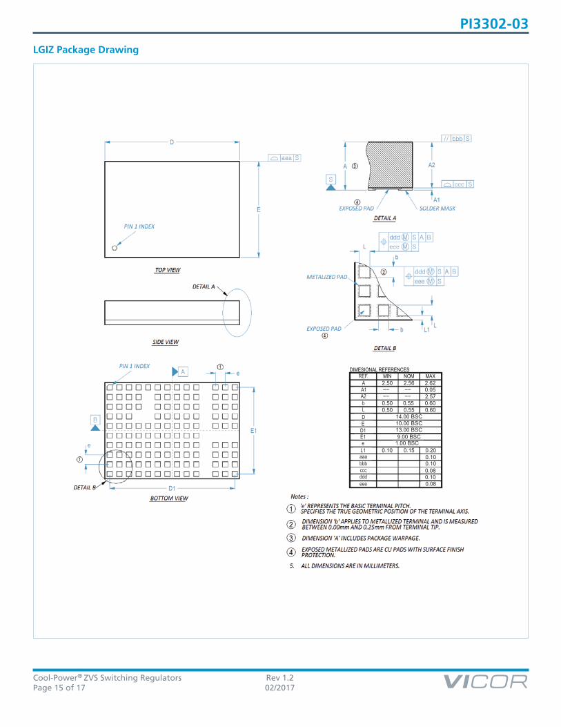
DIMESIONAL REFERENCESNOMMINREF. MAX
AA1A2bL
D1
DE
E1e
L1aaabbbcccdddeee 0.08
2.562.50 2.620.052.57
14.00 BSC
0.550.50 0.60
10.00 BSC13.00 BSC9.00 BSC
1.00 BSC0.150.10 0.20
0.100.100.080.10
0.550.50 0.60
LGIZ Package Drawing
Cool-Power® ZVS Switching Regulators Rev 1.2Page 16 of 17 02/2017
PI3302-03
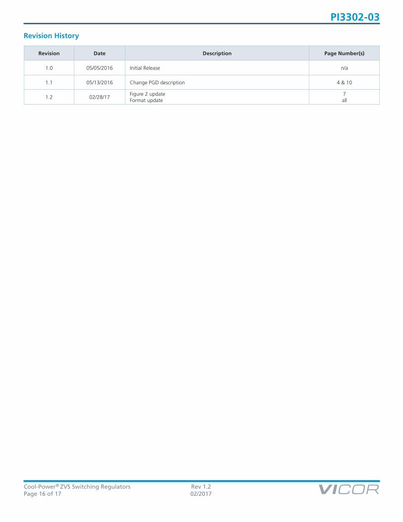
Revision History
Revision Date Description Page Number(s)
1.0 05/05/2016 Initial Release n/a
1.1 05/13/2016 Change PGD description 4 & 10
1.2 02/28/17Figure 2 updateFormat update
7all
Cool-Power® ZVS Switching Regulators Rev 1.2Page 17 of 17 02/2017
PI3302-03
Contact Us: http://www.vicorpower.com/contact-us
Vicor Corporation25 Frontage Road
Andover, MA, USA 01810Tel: 800-735-6200Fax: 978-475-6715
Vicor’s comprehensive line of power solutions includes high density AC-DC and DC-DC modules and accessory components, fully configurable AC-DC and DC-DC power supplies, and complete custom power systems.
Information furnished by Vicor is believed to be accurate and reliable. However, no responsibility is assumed by Vicor for its use. Vicor makes no representations or warranties with respect to the accuracy or completeness of the contents of this publication. Vicor reserves the right to make changes to any products, specifications, and product descriptions at any time without notice. Information published by Vicor has been checked and is believed to be accurate at the time it was printed; however, Vicor assumes no responsibility for inaccuracies. Testing and other quality controls are used to the extent Vicor deems necessary to support Vicor’s product warranty. Except where mandated by government requirements, testing of all parameters of each product is not necessarily performed.
Specifications are subject to change without notice.
Visit http://www.vicorpower.com/dc-dc-converters-board-mount/cool-power-pi33xx-and-pi34xx for the latest product information.
Vicor’s Standard Terms and Conditions and Product WarrantyAll sales are subject to Vicor’s Standard Terms and Conditions of Sale, and Product Warranty which are available on Vicor’s webpage (http://www.vicorpower.com/termsconditionswarranty) or upon request.
Life Support Policy
VICOR’S PRODUCTS ARE NOT AUTHORIZED FOR USE AS CRITICAL COMPONENTS IN LIFE SUPPORT DEVICES OR SYSTEMS WITHOUT THE EXPRESS PRIOR WRITTEN APPROVAL OF THE CHIEF EXECUTIVE OFFICER AND GENERAL COUNSEL OF VICOR CORPORATION. As used herein, life support devices or systems are devices which (a) are intended for surgical implant into the body, or (b) support or sustain life and whose failure to perform when properly used in accordance with instructions for use provided in the labeling can be reasonably expected to result in a significant injury to the user. A critical component is any component in a life support device or system whose failure to perform can be reasonably expected to cause the failure of the life support device or system or to affect its safety or effectiveness. Per Vicor Terms and Conditions of Sale, the user of Vicor products and components in life support applications assumes all risks of such use and indemnifies Vicor against all liability and damages.
Intellectual Property Notice
Vicor and its subsidiaries own Intellectual Property (including issued U.S. and Foreign Patents and pending patent applications) relating to the products described in this data sheet. No license, whether express, implied, or arising by estoppel or otherwise, to any intellectual property rights is granted by this document. Interested parties should contact Vicor’s Intellectual Property Department.
The products described on this data sheet are protected by U.S. Patents. Please see www.vicorpower.com/patents for the latest patent information.