Page 1
8/7/2019 ZVS invererF-1
http://slidepdf.com/reader/full/zvs-invererf-1 1/32
INVERTER BASED ON ZERO VOLTAGEINVERTER BASED ON ZERO VOLTAGE
SWITCHINGSWITCHING
WITH AUXILIARY RESONANT CONVERTER WITH AUXILIARY RESONANT CONVERTER
BRAGHADESWARAN T
LINGADURAI G
MANIKANDAN V BRAJESH GNANADURAI A
GUIDED BY: Mrs.V.Ramya
SUBMITTEDBY:
Page 2
8/7/2019 ZVS invererF-1
http://slidepdf.com/reader/full/zvs-invererf-1 2/32
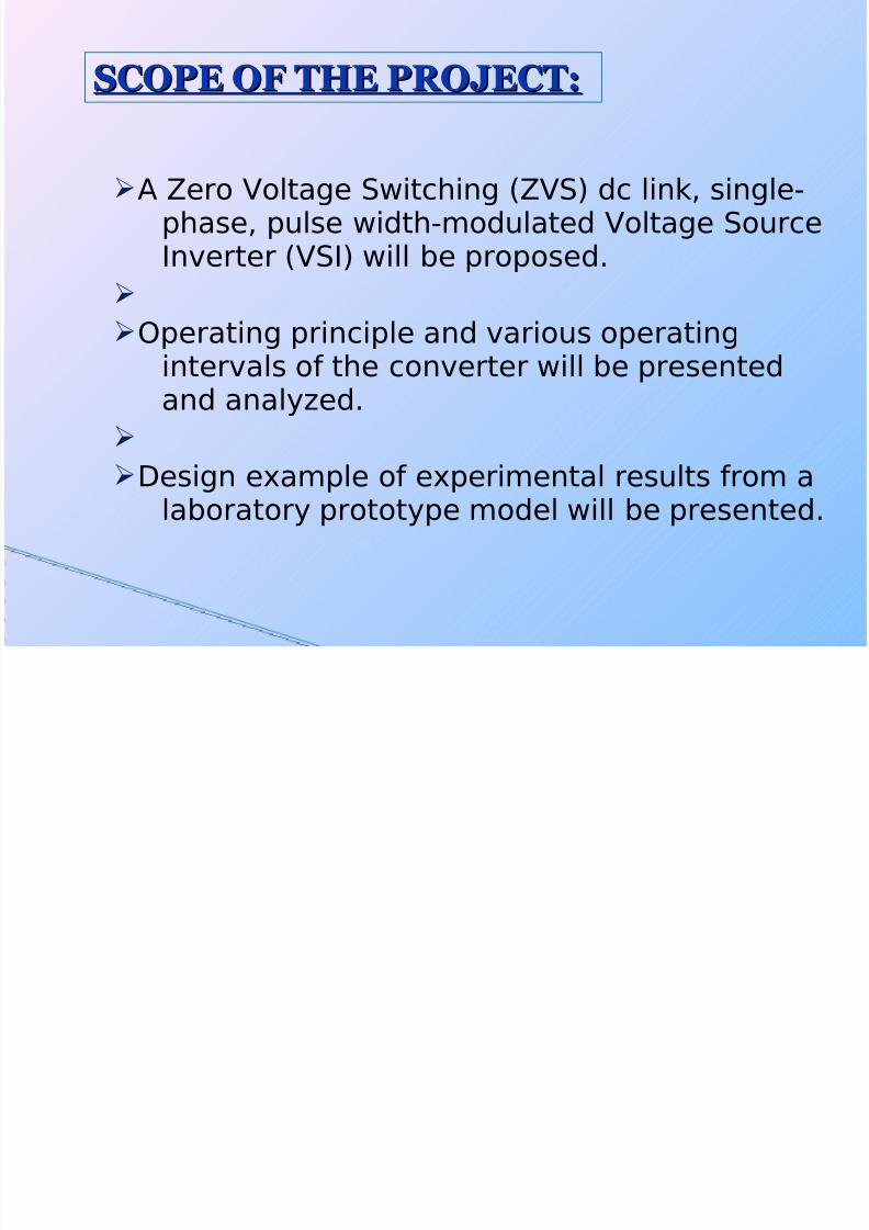
ØA Zero Voltage Switching (ZVS) dc link, single-phase, pulse width-modulated Voltage SourceInverter (VSI) will be proposed.
ØØOperating principle and various operating
intervals of the converter will be presentedand analyzed.
Ø
ØDesign example of experimental results from alaboratory prototype model will be presented.
SCOPE OF THE PROJECT:SCOPE OF THE PROJECT:
Page 3
8/7/2019 ZVS invererF-1
http://slidepdf.com/reader/full/zvs-invererf-1 3/32
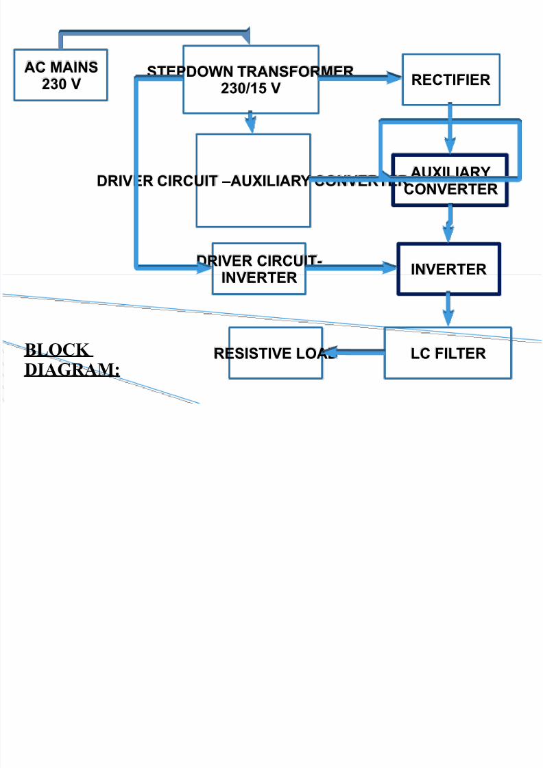
STEPDOWN TRANSFORMER
230/15 V
DRIVER CIRCUIT –AUXILIARY CONVERTER
RECTIFIER
INVERTER
AUXILIARY
CONVERTER
DRIVER CIRCUIT-
INVERTER
RESISTIVE LOAD LC FILTERBLOCK
DIAGRAM:
AC MAINS230 V
Page 4
8/7/2019 ZVS invererF-1
http://slidepdf.com/reader/full/zvs-invererf-1 4/32
ØWide applications - Circuit simplicity andrugged control scheme.
Ø
ØHigh-frequency (HF) operation increases its
switching stress.Ø
ØLimitation to increase the switching frequency -Switching losses.
Ø
ØSignificant turn-on losses in the activeswitches.Ø
ØInput DC source : PWM inverter is fixed DC butnot a controlled one.
Ø
Conventional PWM InverterConventional PWM Inverter
Page 5
8/7/2019 ZVS invererF-1
http://slidepdf.com/reader/full/zvs-invererf-1 5/32
ØReduce the voltage stress to the dc link voltage.
ØØ Soft switching is implemented even with higher
frequency .
Ø
Ø The soft switching for all power factor conditions is
achieved by modifying the carrier for reactivepower-flow conditions.
Ø
ØAll the switches turn-on with zero voltage and theturn-off losses are reduced by lossless capacitive
snubber.
Ø
ØDuring reverse recovery, the di/dt is controlled by theresonant inductor.
Feature of proposed InverterFeature of p
roposed Inverter
Page 6
8/7/2019 ZVS invererF-1
http://slidepdf.com/reader/full/zvs-invererf-1 6/32
ØThe switch voltage is clamped to the dc linkvoltage.
Ø
ØPWM schemes can be used to control the
inverter output voltage.
ØThe PWM modulation scheme is used to obtainoptimum system performance and to
achieve ZVS at different power factorloads.
Ø
ØIt is widely used in variable dc link inverter forimprovement of total harmonic distortionto a minimum level.
Features of Proposed converterFeatures of Prop
osed converter
Page 7
8/7/2019 ZVS invererF-1
http://slidepdf.com/reader/full/zvs-invererf-1 7/32
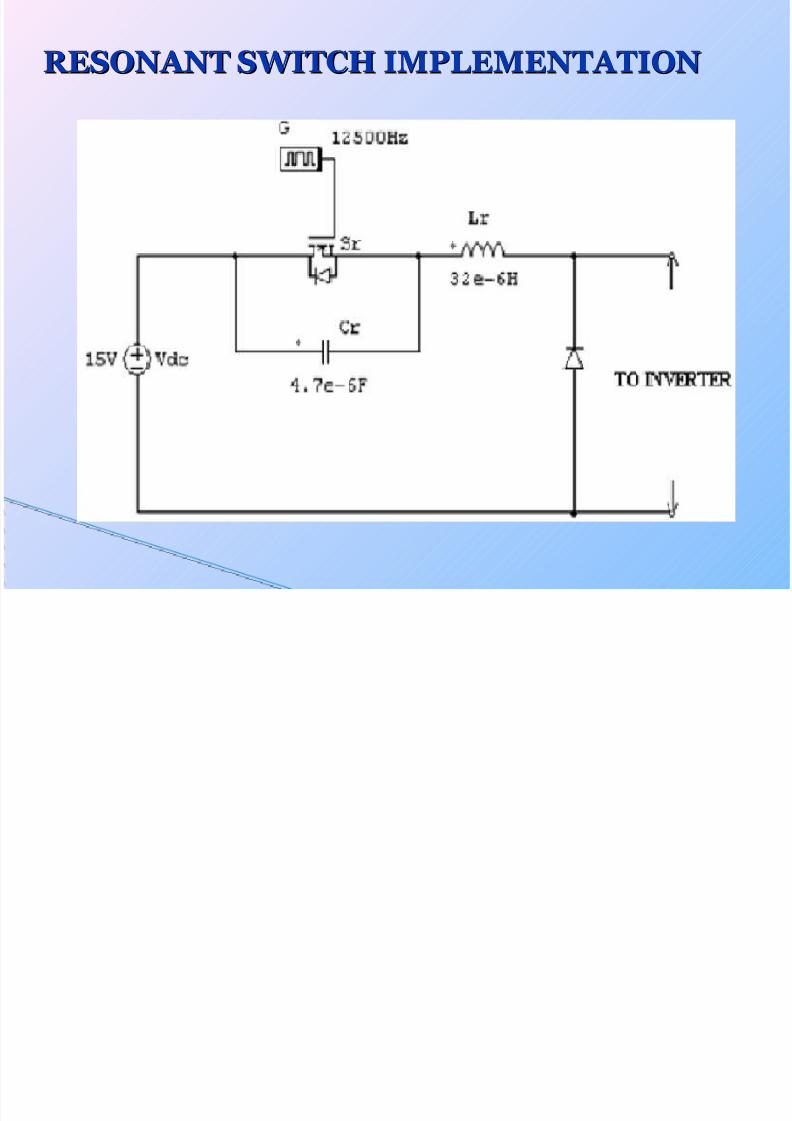
RESONANT SWITCH IMPLEMENTATIONRESONANT SWITCH IMPLEMENTATION
Page 8
8/7/2019 ZVS invererF-1
http://slidepdf.com/reader/full/zvs-invererf-1 8/32
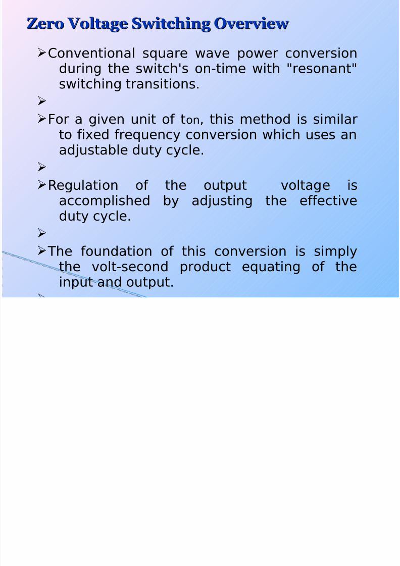
ØConventional square wave power conversion
during the switch's on-time with "resonant"switching transitions.
Ø
ØFor a given unit of ton, this method is similar
to fixed frequency conversion which uses anadjustable duty cycle.
Ø
ØRegulation of the output voltage isaccomplished by adjusting the effectiveduty cycle.
Ø
ØThe foundation of this conversion is simplythe volt-second product equating of the
input and output.
Zero Voltage Switching Overview Zero Voltage Switching Overview
Page 9
8/7/2019 ZVS invererF-1
http://slidepdf.com/reader/full/zvs-invererf-1 9/32
CIRCUIT COMPONENTSCIRCUIT COMPONENTS
Page 10
8/7/2019 ZVS invererF-1
http://slidepdf.com/reader/full/zvs-invererf-1 10/32
HARDWARE SPECIFICATIONHARDWARE SPECIFICATION
AUXILIARY CONVERTER:
Input : 12 volt to 230 volt Maximum of 8 Amps Rating Gate to Source voltage(VGS ) : 10 volt
Carrier frequency (Switching frequency) for
Auxiliary converter : 25KHZ Resonant frequency f r : 12.5 KHz Resonant inductor Lr= 32uH Resonant Capacitor Cr = 4.7uF
DC link Capacitor = 0.22uF MOSFET used is IRFP460
Page 11
8/7/2019 ZVS invererF-1
http://slidepdf.com/reader/full/zvs-invererf-1 11/32
PWM INVERTER:PWM INVERTER:
Input : 12 volt to 230 volt Maximum of 15 Amps Rating
Gate to Source voltage VGS : 10 volt
Carrier frequency (Switching frequency) : 25KHZ MOSFET used is IRFP460
Page 12
8/7/2019 ZVS invererF-1
http://slidepdf.com/reader/full/zvs-invererf-1 12/32
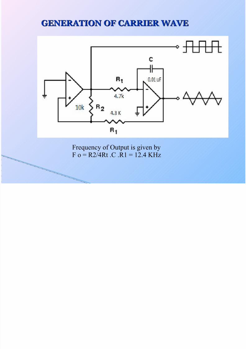
GENERATION OF CARRIER WAVEGENERATION OF CARRIER WAVE
Frequency of Output is given byF o = R2/4Rt .C .R1 = 12.4 KHz
Page 13
8/7/2019 ZVS invererF-1
http://slidepdf.com/reader/full/zvs-invererf-1 13/32
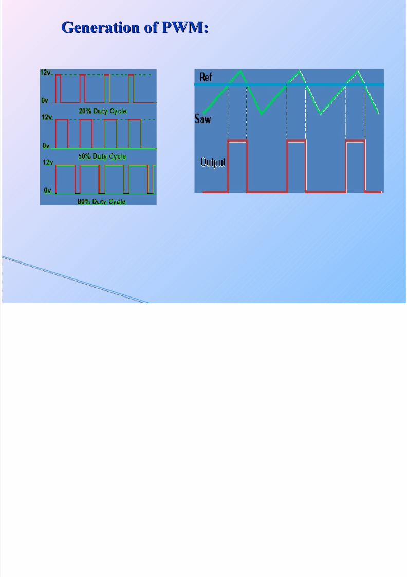
Generation of PWM:Generation of PWM:
Page 14
8/7/2019 ZVS invererF-1
http://slidepdf.com/reader/full/zvs-invererf-1 14/32
PWM Generator :PWM Generator :
Page 15
8/7/2019 ZVS invererF-1
http://slidepdf.com/reader/full/zvs-invererf-1 15/32
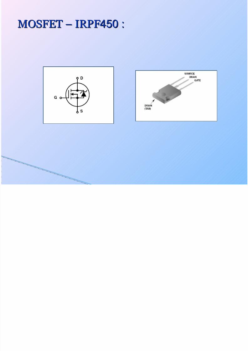
MOSFET – IRPFMOSFET – IRPF450 :450 :
Page 16
8/7/2019 ZVS invererF-1
http://slidepdf.com/reader/full/zvs-invererf-1 16/32
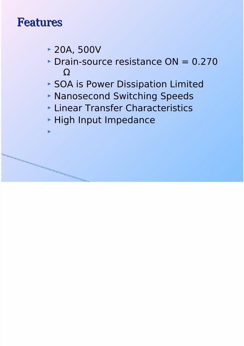
FeaturesFeatures
20A, 500V Drain-source resistance ON = 0.270
Ω
SOA is Power Dissipation Limited Nanosecond Switching Speeds Linear Transfer Characteristics High Input Impedance
Page 17
8/7/2019 ZVS invererF-1
http://slidepdf.com/reader/full/zvs-invererf-1 17/32
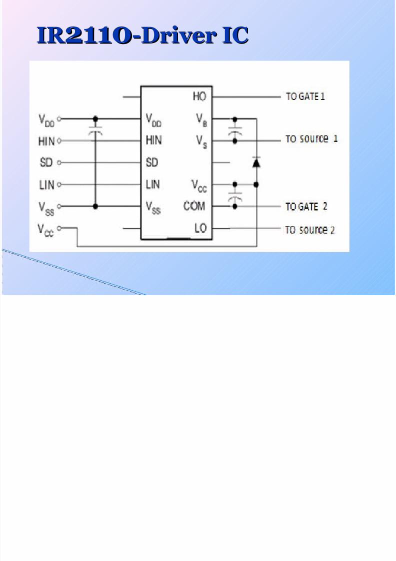
IR IR 21102110-Driver IC-Driver IC
Page 18
8/7/2019 ZVS invererF-1
http://slidepdf.com/reader/full/zvs-invererf-1 18/32
ØIndependent high and low side referenced
output channels.
Ø
ØPropagation delays are matched to simplify usein high frequency applications.
Ø
ØThe floating channel can be used to drive an N-
channel power MOSFET which operates up to500 or 600 volts.
MOSFET Driver Circuit (IR MOSFET Driver Circuit (IR 21102110))
Page 19
8/7/2019 ZVS invererF-1
http://slidepdf.com/reader/full/zvs-invererf-1 19/32
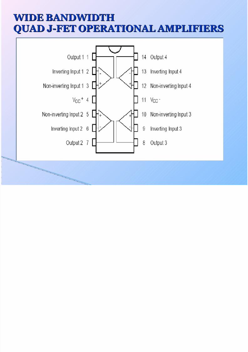
WIDE BANDWIDTHWIDE BANDWIDTHQUAD J-FET OPERATIONAL AMPLIFIERSQUAD J-FET OPERATIONAL AMPLIFIERS
Page 20
8/7/2019 ZVS invererF-1
http://slidepdf.com/reader/full/zvs-invererf-1 20/32
Features:Features:
ØLOW POWER CONSUMPTION
ØLOW INPUT BIAS AND OFFSET CURRENTØØOUTPUTSHORT-CIRCUIT PROTECTION
ØØHIGH INPUT IMPEDANCE JFET INPUT STAGE.
Ø
Page 21
8/7/2019 ZVS invererF-1
http://slidepdf.com/reader/full/zvs-invererf-1 21/32
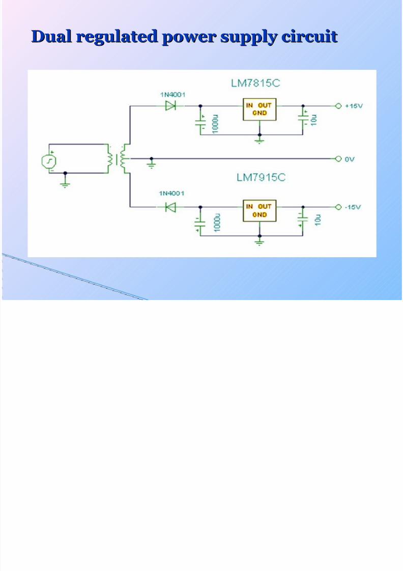
Power supply unitPower supply unit
Page 22
8/7/2019 ZVS invererF-1
http://slidepdf.com/reader/full/zvs-invererf-1 22/32
Dual regulated power supply circuitDual regulated power supply circuit
Page 23
8/7/2019 ZVS invererF-1
http://slidepdf.com/reader/full/zvs-invererf-1 23/32
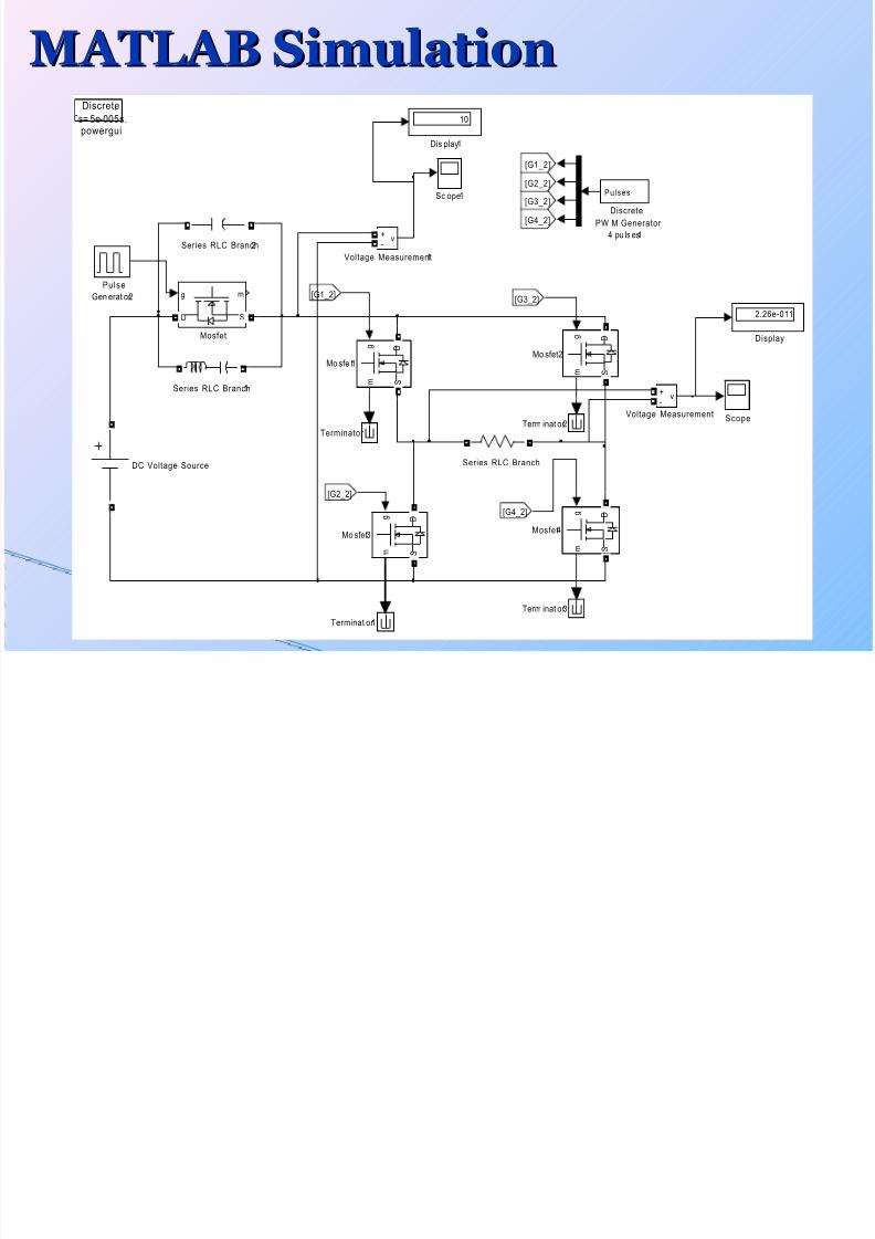
MATLAB SIMULATIONMATLAB SIMULATION
Page 24
8/7/2019 ZVS invererF-1
http://slidepdf.com/reader/full/zvs-invererf-1 24/32
MATLAB SimulationMATLAB Simulation
powergui
Discrete,
s= 5e-005 s.
Voltage Measurement1
v+-
Voltage Measurement
v+-
Term inat or3
Term inat or2
Terminat or1
Terminator
Series RLC Branch2
Series RLC Branch1
Series RLC Branch
Sc ope1
Scope
Pulse
Gen erat or2
Mosfet4
g
m
D
S
Mo sfet3
g
m
D
S
Mo sfet2
g
m
D
S
Mo sfe t1
g
m
D
S
Mosfet
g m
D S
[G4_2]
[G3_2]
[G2_2]
[G1_2]
[G4_2]
[G3_2]
[G2_2]
[G1_2]
Dis play1
10
Display
2.26e-011
Discrete
PW M Generator
4 pu ls es1
Pulses
DC Voltage Source
Page 25
8/7/2019 ZVS invererF-1
http://slidepdf.com/reader/full/zvs-invererf-1 25/32
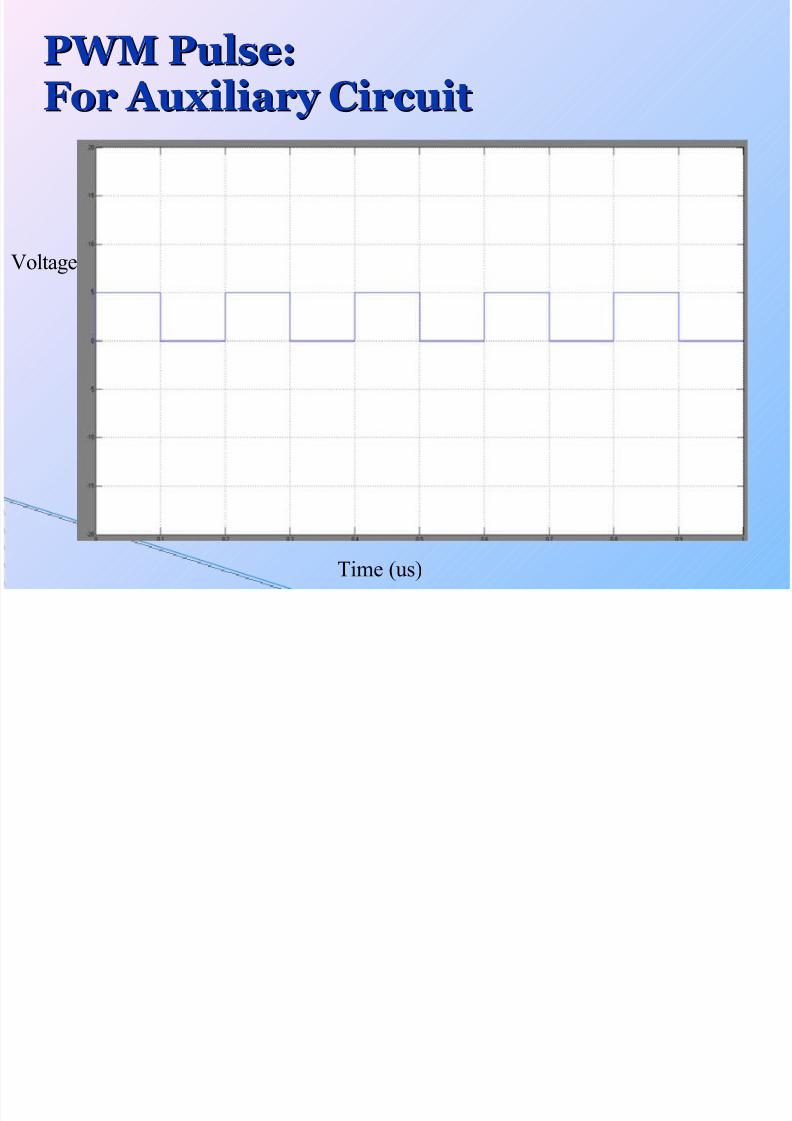
PWM Pulse:PWM Pulse:For Auxiliary CircuitFor Auxiliary Circuit
Time (us)
Voltage
Page 26
8/7/2019 ZVS invererF-1
http://slidepdf.com/reader/full/zvs-invererf-1 26/32
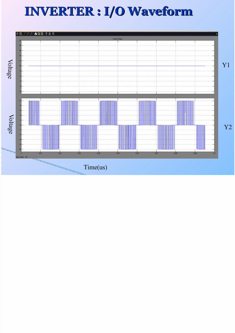
INVERTER : I/O WaveformINVERTER : I/O Waveform
Y1
Y2
Vol t a ge
Time(us)
Vo
l t a ge
Page 27
8/7/2019 ZVS invererF-1
http://slidepdf.com/reader/full/zvs-invererf-1 27/32
Input And Output Of The Converter:Input And Output Of The Converter:
Time(us)
vol t a ge
Page 28
8/7/2019 ZVS invererF-1
http://slidepdf.com/reader/full/zvs-invererf-1 28/32
Used in Un-Interrupted Power Supply.
Used in High Frequency SwitchingConverter.
Used in Industrial Drives.
Solar inverter.
ApplicationsApplications
Page 29
8/7/2019 ZVS invererF-1
http://slidepdf.com/reader/full/zvs-invererf-1 29/32
Only one extra switch is required in the dc link toobtain ZVS.
Experimental results confirm the soft switching
characteristics of the proposed VSI.
An experimental prototype laboratory model of 300 VA, 120 V, 60 Hz, VSI operating at 50 kHz
is implemented using MOSFETs.
CONCLUSIONCONCLUSION
Page 30
8/7/2019 ZVS invererF-1
http://slidepdf.com/reader/full/zvs-invererf-1 30/32
Limitations - trade-offs betweenfrequency and output power.
Output of inverter can be remotelycontrolled.
Higher switching frequency requires correctuse of the resonant network circuitimplementation.
Packaging of converters with reducedstray inductance and size - Greatercommercialization of these converters.
Future Scope:Future Scope:
Page 31
8/7/2019 ZVS invererF-1
http://slidepdf.com/reader/full/zvs-invererf-1 31/32
Ø Agelidis V.G., P. D. Ziogas, and G. Joos, “An optimummodulation strategy for a novel notch commutated 3-phase PWM inverter,”.
Ø
Ø Bellar M. D., T. S.Wu, A. Tchamdjou, J. Mahdavi, and M.
Ehsani, “A review of soft switched DC-AC converters,”.
Ø Divan D. M., “The resonant dc link converterA newconcept in static power conversion,”.
Ø Oh. I. and M. J. Youn, “A simple soft switched PWMinverter using
source voltage clamped resonant circuit,”.
Ø Wang K., Y. Jiang, S. Dubovsky, G. Hua, D. Boroyevich,and F. C. Lee, “Novel Dc-Rail soft switched three phase
voltage source inverters,”.Ø
ReferencesReferences
Page 32
8/7/2019 ZVS invererF-1
http://slidepdf.com/reader/full/zvs-invererf-1 32/32
Thank you.